%45%6c%65%63%74%72%69%63%61%6c%20%45%6e%67%69%6e%65%65%72%69%6e%67
-
 KAIST Overcomes Limitations of Existing Image Sensors… Clear Colors Even Under Oblique Light
<(From Left) Ph.D candidate Chanhyung Park from Electrical Engineering, Jaehyun Jeon from Department of Physics, Professor Min Seok Jang from Electrical Engineering>
Smartphone cameras are becoming smaller, yet photos are becoming sharper. Korean researchers have elevated the limits of next-generation smartphone cameras by developing a new image sensor technology that can accurately represent colors regardless of the angle at which light enters. The team achieved this by utilizing a “metamaterial” that designs the movement of light through structures too small to be seen with the naked eye.
KAIST (President Kwang Hyung Lee) announced on the 12th of February that a research team led by Professor Min Seok Jang of the School of Electrical Engineering, in collaboration with Professor Haejun Chung’s team at Hanyang, has developed a metamaterial-based technology for image sensors that can stably separate colors even when the angle of light incidence varies.
Conventional smartphone cameras capture images by concentrating light into a small lens. However, as camera pixels become extremely small, lenses alone struggle to gather sufficient light. To address this, the Nanophotonic Color Router was introduced. Instead of concentrating light through a lens, this technology uses microscopic structures invisible to the eye to precisely separate incoming light by color. By designing the pathways through which light travels, this metamaterial-based structure accurately divides light into red (R), green (G), and blue (B).
Samsung Electronics has already demonstrated the commercialization potential of this technology by applying it to actual image sensors under the name “Nano Prism.” Theoretically, stacking multiple layers of extremely fine nanostructures enables greater light collection and more accurate color separation.
<Nanophotonic color router technology that works reliably even under oblique incidence conditions (AI-generated image)>
However, existing Nanophotonic Color Routers had limitations. While they functioned well when light entered vertically, their performance deteriorated significantly—or colors mixed—when light entered at an angle, as is common in smartphone cameras. This issue, known as the “oblique incidence problem,” has been considered a critical challenge that must be resolved for real-world product applications.
The research team first investigated the root cause of this issue. They found that previous designs were overly optimized for vertically incident light, causing performance to drop sharply even with slight changes in the angle of incidence. Since smartphone cameras receive light from various angles, maintaining performance under angular variation is essential.
Instead of manually designing the structure, the team adopted an “inverse design” approach, which allows the computer to autonomously determine the optimal structure. Through this method, they derived a color router design capable of stable color separation even when the angle of incoming light changes.
As a result, whereas previous structures nearly failed when light was tilted by about 12 degrees, the newly designed structure maintained approximately 78% optical efficiency within a ±12-degree range, demonstrating stable color separation performance. In other words, the technology reaches a level suitable for practical smartphone usage environments.
<Nanophotonic color router robust to oblique incidence>
The team further analyzed performance variations by considering factors such as the number of metamaterial layers, design conditions, and potential fabrication errors. They also systematically defined the limits of robustness against changes in the angle of incidence. This study is particularly meaningful in that it presents design criteria for color routers that reflect realistic image sensor environments.
Professor Min Seok Jang of KAIST stated, “This research is significant in that it systematically analyzes the oblique incidence problem, which has hindered the commercialization of color router technology, and proposes a clear solution direction,” adding, “The proposed design methodology can be extended beyond color routers to a wide range of metamaterial-based nanophotonic devices.”
In this study, KAIST undergraduate student Jaehyun Jeon and doctoral candidate Chanhyung Park participated as co-first authors. The research findings were published on January 27 in the international journal Advanced Optical Materials.
※ Paper title: “Inverse Design of Nanophotonic Color Router Robust to Oblique Incidence”
DOI: https://doi.org/10.1002/adom.202501697※ Authors: Jaehyun Jeon (KAIST, first author), Chanhyung Park (KAIST, first author), Doyoung Heo (KAIST), Haejun Chung (Hanyang University), Min Seok Jang (KAIST, corresponding author)
This research was supported by the Ministry of Trade, Industry & Energy (Korea Institute for Advancement of Technology, Korea Semiconductor Research Consortium) under the project “Design Technology of Meta-Optical Structures for Next-Generation Sensors,” by the Ministry of Science and ICT (National Research Foundation of Korea) under the projects “Development of Full-Color Micro LED Devices and Panels Based on Beam-Steerable High-Color-Purity Meta Color Conversion Layers” and “Development of a Real-Time Zero-Energy Argos-Eye Metasurface Network Computing with All Properties of Light,” and by the Ministry of Culture, Sports and Tourism (Korea Creative Content Agency) under the project “International Joint Research for Next-Generation Copyright Protection and Secure Content Distribution Technologies.”
2026.02.19 View 1576
KAIST Overcomes Limitations of Existing Image Sensors… Clear Colors Even Under Oblique Light
<(From Left) Ph.D candidate Chanhyung Park from Electrical Engineering, Jaehyun Jeon from Department of Physics, Professor Min Seok Jang from Electrical Engineering>
Smartphone cameras are becoming smaller, yet photos are becoming sharper. Korean researchers have elevated the limits of next-generation smartphone cameras by developing a new image sensor technology that can accurately represent colors regardless of the angle at which light enters. The team achieved this by utilizing a “metamaterial” that designs the movement of light through structures too small to be seen with the naked eye.
KAIST (President Kwang Hyung Lee) announced on the 12th of February that a research team led by Professor Min Seok Jang of the School of Electrical Engineering, in collaboration with Professor Haejun Chung’s team at Hanyang, has developed a metamaterial-based technology for image sensors that can stably separate colors even when the angle of light incidence varies.
Conventional smartphone cameras capture images by concentrating light into a small lens. However, as camera pixels become extremely small, lenses alone struggle to gather sufficient light. To address this, the Nanophotonic Color Router was introduced. Instead of concentrating light through a lens, this technology uses microscopic structures invisible to the eye to precisely separate incoming light by color. By designing the pathways through which light travels, this metamaterial-based structure accurately divides light into red (R), green (G), and blue (B).
Samsung Electronics has already demonstrated the commercialization potential of this technology by applying it to actual image sensors under the name “Nano Prism.” Theoretically, stacking multiple layers of extremely fine nanostructures enables greater light collection and more accurate color separation.
<Nanophotonic color router technology that works reliably even under oblique incidence conditions (AI-generated image)>
However, existing Nanophotonic Color Routers had limitations. While they functioned well when light entered vertically, their performance deteriorated significantly—or colors mixed—when light entered at an angle, as is common in smartphone cameras. This issue, known as the “oblique incidence problem,” has been considered a critical challenge that must be resolved for real-world product applications.
The research team first investigated the root cause of this issue. They found that previous designs were overly optimized for vertically incident light, causing performance to drop sharply even with slight changes in the angle of incidence. Since smartphone cameras receive light from various angles, maintaining performance under angular variation is essential.
Instead of manually designing the structure, the team adopted an “inverse design” approach, which allows the computer to autonomously determine the optimal structure. Through this method, they derived a color router design capable of stable color separation even when the angle of incoming light changes.
As a result, whereas previous structures nearly failed when light was tilted by about 12 degrees, the newly designed structure maintained approximately 78% optical efficiency within a ±12-degree range, demonstrating stable color separation performance. In other words, the technology reaches a level suitable for practical smartphone usage environments.
<Nanophotonic color router robust to oblique incidence>
The team further analyzed performance variations by considering factors such as the number of metamaterial layers, design conditions, and potential fabrication errors. They also systematically defined the limits of robustness against changes in the angle of incidence. This study is particularly meaningful in that it presents design criteria for color routers that reflect realistic image sensor environments.
Professor Min Seok Jang of KAIST stated, “This research is significant in that it systematically analyzes the oblique incidence problem, which has hindered the commercialization of color router technology, and proposes a clear solution direction,” adding, “The proposed design methodology can be extended beyond color routers to a wide range of metamaterial-based nanophotonic devices.”
In this study, KAIST undergraduate student Jaehyun Jeon and doctoral candidate Chanhyung Park participated as co-first authors. The research findings were published on January 27 in the international journal Advanced Optical Materials.
※ Paper title: “Inverse Design of Nanophotonic Color Router Robust to Oblique Incidence”
DOI: https://doi.org/10.1002/adom.202501697※ Authors: Jaehyun Jeon (KAIST, first author), Chanhyung Park (KAIST, first author), Doyoung Heo (KAIST), Haejun Chung (Hanyang University), Min Seok Jang (KAIST, corresponding author)
This research was supported by the Ministry of Trade, Industry & Energy (Korea Institute for Advancement of Technology, Korea Semiconductor Research Consortium) under the project “Design Technology of Meta-Optical Structures for Next-Generation Sensors,” by the Ministry of Science and ICT (National Research Foundation of Korea) under the projects “Development of Full-Color Micro LED Devices and Panels Based on Beam-Steerable High-Color-Purity Meta Color Conversion Layers” and “Development of a Real-Time Zero-Energy Argos-Eye Metasurface Network Computing with All Properties of Light,” and by the Ministry of Culture, Sports and Tourism (Korea Creative Content Agency) under the project “International Joint Research for Next-Generation Copyright Protection and Secure Content Distribution Technologies.”
2026.02.19 View 1576 -
 KAIST Confirms Reduction of Amyloid-β Using Red OLED-Restores Memory in Alzheimer’s Model
<Professor Kyung Cheol Choi, Dr. Byeongju Noh, Ph.D candidate Young-Hun Jung, Ph.D candidate Minwoo Park, Dr.Ja Wook Koo, Researcher Jiyun Lee, Researcher Ji-Eun Lee, Dr. Hyang Sook Hoe, Dr. Hyun-Ju Lee, Dr. Sora Kang, Researcher Seokjun Oh>
A Korean research team, raising the question “Which OLED light color can actually improve memory and pathological markers in Alzheimer’s patients?”, has identified the most effective OLED color capable of enhancing cognitive function using only light—with no drugs involved. The OLED platform developed for this study can precisely control color, brightness, flicker frequency, and exposure duration, suggesting potential future development into personalized OLED-based electroceuticals.
On the 24th, KAIST (President Kwang Hyung Lee) announced that a joint research team led by Professor Kyung Cheol Choi from the School of Electrical Engineering at KAIST and Dr. Ja Wook Koo and Dr. Hyang Sook Hoe from the Korea Brain Research Institute (KBRI) developed a uniform-illuminance, three-color OLED photostimulation technology and confirmed that “red 40-Hz light” was the most effective among blue, green, and red in improving Alzheimer's pathology and memory function.
To overcome the structural limitations of conventional LEDs—such as brightness imbalance, heat generation risk, and variability caused by animal movement—the researchers developed an OLED-based photostimulation platform that emits light uniformly. Using this platform, they compared white, red, green, and blue light under identical conditions (40-Hz frequency, brightness, and exposure time) and found that red 40-Hz light produced the most significant improvement.
In an early-stage (3-month-old) Alzheimer’s animal model, improvement in pathology and memory was observed after only two days of stimulation. When early Alzheimer’s model mice were exposed to one hour of light per day for two days, both white and red light improved long-term memory. Additionally, the amount of amyloid-β (Aβ) plaques—protein aggregates known as a major factor in Alzheimer’s disease—was reduced in key brain regions such as the hippocampus, and levels of the plaque-clearing enzyme ADAM17 increased.
This indicates that even very short periods of light stimulation can reduce harmful proteins in the brain and improve memory function. In particular, with red light, the inflammatory cytokine IL-1β, known to exacerbate inflammation and contribute to Alzheimer’s progression, decreased significantly, demonstrating an anti-inflammatory effect.
Moreover, the more plaque was reduced, the greater the improvement in memory—direct evidence that pathological improvement leads to cognitive enhancement.
In the mid-stage (6-month-old) Alzheimer’s model, statistically significant pathological improvement was seen only with red light. In a two-week long-term stimulation experiment under the same conditions, both white and red light improved memory, but a statistically meaningful reduction in plaques appeared only under red light.
< The mechanism by which red OLED stimulation of neurons reduces amyloid-β in Alzheimer’s model mice >
Differences at the molecular level were also clear. Under red light, levels of ADAM17 (which helps remove plaques) increased, while levels of BACE1, an enzyme responsible for producing plaques, decreased—demonstrating a dual effect of both inhibiting plaque formation and promoting plaque removal. In contrast, white light only lowered BACE1, showing more limited therapeutic effects compared to red light.
This scientifically identifies that the color of light is a key factor determining therapeutic efficacy.
To determine which neural circuits were activated by light stimulation, the team analyzed the expression of c-Fos, an immediate-early gene that is activated when neurons fire.
They found activation throughout the visual–memory circuit, extending from the visual cortex → thalamus → hippocampus, providing direct neurological evidence that light stimulation awakens the visual pathway, enhancing hippocampal function and memory.
Thanks to the uniform-illuminance OLED platform, light was evenly delivered regardless of animal movement, ensuring stable experimental results and high reproducibility across repeated tests.
This study is the first to demonstrate that cognitive function can be improved using only light, without drugs, and that Alzheimer’s pathological markers can be regulated through combinations of light color, frequency, and duration.
The OLED platform developed in this study allows fine control over color, brightness, flicker ratio, and exposure time, making it suitable for personalized stimulation design in future human clinical research.
The research team plans to expand conditions such as stimulation intensity, energy, duration, and combined visual–auditory stimulation, aiming toward clinical-stage development.
Dr. Byeongju Noh (from Professor Kyung Cheol Choi’s research team) said, “This study experimentally demonstrates the importance of color standardization and confirms that red OLED is the key color that activates ADAM17 and suppresses BACE1 across disease stages.”
Professor Kyung Cheol Choi emphasized, “Our uniform-illuminance OLED platform overcomes the structural limitations of traditional LEDs and enables high reproducibility and safe evaluation. We expect wearable RED OLED electroceuticals for everyday use to present a new therapeutic paradigm for Alzheimer’s disease.”
The research findings were published online on October 25 in ACS Biomaterials Science & Engineering, a leading international journal in biomedical and materials science.
Paper Title: Color Dependence of OLED Phototherapy for Cognitive Function and Beta-Amyloid Reduction through ADAM17 and BACE1
DOI: https://pubs.acs.org/doi/full/10.1021/acsbiomaterials.5c01162
Co-authors:Byeongju Noh, Hyun-Ju Lee, Jiyun Lee, Jiyun Lee, Ji-Eun Lee, Bitna Joo, Young-Hun Jung, Minwoo Park, Sora Kang, Seokjun Oh, Jeong-Woo Hwang, Dae-Si Kang, Yongmin Jeon, So-Min Lee, Hyang Sook Hoe, Ja Wook Koo, Kyung Cheol Choi
This research was supported by the National Research Foundation of Korea and the National IT Industry Promotion Agency under the Ministry of Science and ICT, and the Korea Brain Research Institute Basic Research Program. (2017R1A5A1014708, 2022M3E5E9018226, H0501-25-1001, 25-BR-02-02, 25-BR-02-04)
2025.11.24 View 2258
KAIST Confirms Reduction of Amyloid-β Using Red OLED-Restores Memory in Alzheimer’s Model
<Professor Kyung Cheol Choi, Dr. Byeongju Noh, Ph.D candidate Young-Hun Jung, Ph.D candidate Minwoo Park, Dr.Ja Wook Koo, Researcher Jiyun Lee, Researcher Ji-Eun Lee, Dr. Hyang Sook Hoe, Dr. Hyun-Ju Lee, Dr. Sora Kang, Researcher Seokjun Oh>
A Korean research team, raising the question “Which OLED light color can actually improve memory and pathological markers in Alzheimer’s patients?”, has identified the most effective OLED color capable of enhancing cognitive function using only light—with no drugs involved. The OLED platform developed for this study can precisely control color, brightness, flicker frequency, and exposure duration, suggesting potential future development into personalized OLED-based electroceuticals.
On the 24th, KAIST (President Kwang Hyung Lee) announced that a joint research team led by Professor Kyung Cheol Choi from the School of Electrical Engineering at KAIST and Dr. Ja Wook Koo and Dr. Hyang Sook Hoe from the Korea Brain Research Institute (KBRI) developed a uniform-illuminance, three-color OLED photostimulation technology and confirmed that “red 40-Hz light” was the most effective among blue, green, and red in improving Alzheimer's pathology and memory function.
To overcome the structural limitations of conventional LEDs—such as brightness imbalance, heat generation risk, and variability caused by animal movement—the researchers developed an OLED-based photostimulation platform that emits light uniformly. Using this platform, they compared white, red, green, and blue light under identical conditions (40-Hz frequency, brightness, and exposure time) and found that red 40-Hz light produced the most significant improvement.
In an early-stage (3-month-old) Alzheimer’s animal model, improvement in pathology and memory was observed after only two days of stimulation. When early Alzheimer’s model mice were exposed to one hour of light per day for two days, both white and red light improved long-term memory. Additionally, the amount of amyloid-β (Aβ) plaques—protein aggregates known as a major factor in Alzheimer’s disease—was reduced in key brain regions such as the hippocampus, and levels of the plaque-clearing enzyme ADAM17 increased.
This indicates that even very short periods of light stimulation can reduce harmful proteins in the brain and improve memory function. In particular, with red light, the inflammatory cytokine IL-1β, known to exacerbate inflammation and contribute to Alzheimer’s progression, decreased significantly, demonstrating an anti-inflammatory effect.
Moreover, the more plaque was reduced, the greater the improvement in memory—direct evidence that pathological improvement leads to cognitive enhancement.
In the mid-stage (6-month-old) Alzheimer’s model, statistically significant pathological improvement was seen only with red light. In a two-week long-term stimulation experiment under the same conditions, both white and red light improved memory, but a statistically meaningful reduction in plaques appeared only under red light.
< The mechanism by which red OLED stimulation of neurons reduces amyloid-β in Alzheimer’s model mice >
Differences at the molecular level were also clear. Under red light, levels of ADAM17 (which helps remove plaques) increased, while levels of BACE1, an enzyme responsible for producing plaques, decreased—demonstrating a dual effect of both inhibiting plaque formation and promoting plaque removal. In contrast, white light only lowered BACE1, showing more limited therapeutic effects compared to red light.
This scientifically identifies that the color of light is a key factor determining therapeutic efficacy.
To determine which neural circuits were activated by light stimulation, the team analyzed the expression of c-Fos, an immediate-early gene that is activated when neurons fire.
They found activation throughout the visual–memory circuit, extending from the visual cortex → thalamus → hippocampus, providing direct neurological evidence that light stimulation awakens the visual pathway, enhancing hippocampal function and memory.
Thanks to the uniform-illuminance OLED platform, light was evenly delivered regardless of animal movement, ensuring stable experimental results and high reproducibility across repeated tests.
This study is the first to demonstrate that cognitive function can be improved using only light, without drugs, and that Alzheimer’s pathological markers can be regulated through combinations of light color, frequency, and duration.
The OLED platform developed in this study allows fine control over color, brightness, flicker ratio, and exposure time, making it suitable for personalized stimulation design in future human clinical research.
The research team plans to expand conditions such as stimulation intensity, energy, duration, and combined visual–auditory stimulation, aiming toward clinical-stage development.
Dr. Byeongju Noh (from Professor Kyung Cheol Choi’s research team) said, “This study experimentally demonstrates the importance of color standardization and confirms that red OLED is the key color that activates ADAM17 and suppresses BACE1 across disease stages.”
Professor Kyung Cheol Choi emphasized, “Our uniform-illuminance OLED platform overcomes the structural limitations of traditional LEDs and enables high reproducibility and safe evaluation. We expect wearable RED OLED electroceuticals for everyday use to present a new therapeutic paradigm for Alzheimer’s disease.”
The research findings were published online on October 25 in ACS Biomaterials Science & Engineering, a leading international journal in biomedical and materials science.
Paper Title: Color Dependence of OLED Phototherapy for Cognitive Function and Beta-Amyloid Reduction through ADAM17 and BACE1
DOI: https://pubs.acs.org/doi/full/10.1021/acsbiomaterials.5c01162
Co-authors:Byeongju Noh, Hyun-Ju Lee, Jiyun Lee, Jiyun Lee, Ji-Eun Lee, Bitna Joo, Young-Hun Jung, Minwoo Park, Sora Kang, Seokjun Oh, Jeong-Woo Hwang, Dae-Si Kang, Yongmin Jeon, So-Min Lee, Hyang Sook Hoe, Ja Wook Koo, Kyung Cheol Choi
This research was supported by the National Research Foundation of Korea and the National IT Industry Promotion Agency under the Ministry of Science and ICT, and the Korea Brain Research Institute Basic Research Program. (2017R1A5A1014708, 2022M3E5E9018226, H0501-25-1001, 25-BR-02-02, 25-BR-02-04)
2025.11.24 View 2258 -
 IEEE President Professor Kramer Holds Special Lecture on Artificial Intelligence in the Electrical Engineering Department
Kathleen A. Kramer, President of the IEEE (Institute of Electrical and Electronics Engineers), the world's largest technical professional organization dedicated to electrical and electronic technology, visited our university on the 30th and delivered a special lecture under the theme, 'Drawing the Future of Artificial Intelligence Together.'
< IEEE Leadership and KAIST EE Meeting KITIS Director (Sung-Hyun Hong), KAIST EE Professors (Joonwoo Bae), (Ian Oakley), (Hye-Won Jeong), (Chang-Shik Choi), (Dong-Soo Han), Head of EE Department (Seunghyup Yoo), IEEE President (Kathleen A. Kramer), IEEE Senior Sales Director (Francis Staples), IEEE Regional Manager for APAC (Ira Tan), KAIST EE Professor (Hee-Jin Ahn), Head of Semiconductor System Engineering Department (Sung-Hwan Cho)>
Standing at the colloquium podium by invitation of the Department of Electrical Engineering (Head: Seung-Hyup Yoo), President Kramer emphasized based on IEEE's core vision, 'Advancing Technology for Humanity,' that "Artificial Intelligence (AI) is no longer a concept of the distant future; it has become a technology that is transforming human lives at the center of innovation."
< Photo of IEEE President's KAIST EE Colloquium Lecture >
She further added, "Technology must advance with human values at its core, and AI based on ethics and inclusiveness can lead to true innovation," sharing her insights on the direction of AI development and the social responsibility of technology.
Seung-Hyup Yoo, Head of the Department of Electrical Engineering, stated, "We expect President Kramer's visit to be a stepping stone that will not only widely promote our department's capabilities in advanced fields such as AI, semiconductors, signal processing, and robotics to the international academic community but also strengthen cooperation in various ways."
< Tea Meeting with the IEEE Leadership and the Vice Presidents . KITIS Director (Sung-Hyun Hong), IEEE Senior Sales Director (Francis Staples), IEEE President (Kathleen A. Kramer), KAIST Executive Vice President for Research (Sang Yup Lee), Head of EE Department (Seunghyup Yoo), IEEE Regional Manager for APAC (Ira Tan)>
Meanwhile, prior to the lecture, President Kramer paid a courtesy visit to Sang-Yup Lee, KAIST Executive Vice President for Research, and reaffirmed the commitment of both organizations to advancing sustainable technology and building an ethical and inclusive research ecosystem to contribute to a better life for humanity.
2025.11.06 View 1659
IEEE President Professor Kramer Holds Special Lecture on Artificial Intelligence in the Electrical Engineering Department
Kathleen A. Kramer, President of the IEEE (Institute of Electrical and Electronics Engineers), the world's largest technical professional organization dedicated to electrical and electronic technology, visited our university on the 30th and delivered a special lecture under the theme, 'Drawing the Future of Artificial Intelligence Together.'
< IEEE Leadership and KAIST EE Meeting KITIS Director (Sung-Hyun Hong), KAIST EE Professors (Joonwoo Bae), (Ian Oakley), (Hye-Won Jeong), (Chang-Shik Choi), (Dong-Soo Han), Head of EE Department (Seunghyup Yoo), IEEE President (Kathleen A. Kramer), IEEE Senior Sales Director (Francis Staples), IEEE Regional Manager for APAC (Ira Tan), KAIST EE Professor (Hee-Jin Ahn), Head of Semiconductor System Engineering Department (Sung-Hwan Cho)>
Standing at the colloquium podium by invitation of the Department of Electrical Engineering (Head: Seung-Hyup Yoo), President Kramer emphasized based on IEEE's core vision, 'Advancing Technology for Humanity,' that "Artificial Intelligence (AI) is no longer a concept of the distant future; it has become a technology that is transforming human lives at the center of innovation."
< Photo of IEEE President's KAIST EE Colloquium Lecture >
She further added, "Technology must advance with human values at its core, and AI based on ethics and inclusiveness can lead to true innovation," sharing her insights on the direction of AI development and the social responsibility of technology.
Seung-Hyup Yoo, Head of the Department of Electrical Engineering, stated, "We expect President Kramer's visit to be a stepping stone that will not only widely promote our department's capabilities in advanced fields such as AI, semiconductors, signal processing, and robotics to the international academic community but also strengthen cooperation in various ways."
< Tea Meeting with the IEEE Leadership and the Vice Presidents . KITIS Director (Sung-Hyun Hong), IEEE Senior Sales Director (Francis Staples), IEEE President (Kathleen A. Kramer), KAIST Executive Vice President for Research (Sang Yup Lee), Head of EE Department (Seunghyup Yoo), IEEE Regional Manager for APAC (Ira Tan)>
Meanwhile, prior to the lecture, President Kramer paid a courtesy visit to Sang-Yup Lee, KAIST Executive Vice President for Research, and reaffirmed the commitment of both organizations to advancing sustainable technology and building an ethical and inclusive research ecosystem to contribute to a better life for humanity.
2025.11.06 View 1659 -
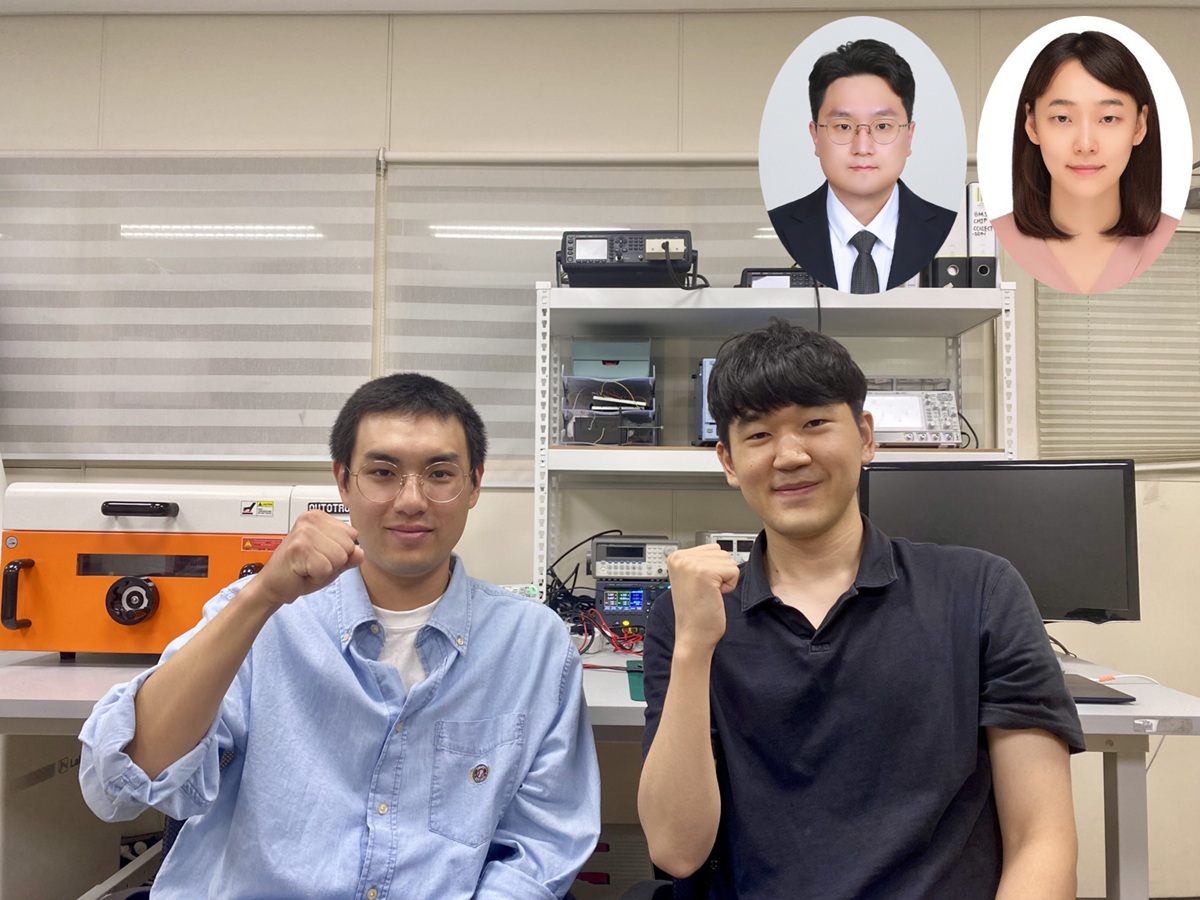
 KAIST Researchers Uncover Critical Security Flaws in Global Mobile Networks
Breakthrough Discovery Reveals How Attackers Can Remotely Manipulate User Data Without Physical Proximity
DAEJEON, South Korea — In an era when recent cyberattacks on major telecommunications providers have highlighted the fragility of mobile security, researchers at the Korea Advanced Institute of Science and Technology have identified a class of previously unknown vulnerabilities that could allow remote attackers to compromise cellular networks serving billions of users worldwide.
The research team, led by Professor Yongdae Kim of KAIST's School of Electrical Engineering, discovered that unauthorized attackers could remotely manipulate internal user information in LTE core networks — the central infrastructure that manages authentication, internet connectivity, and data transmission for mobile devices and IoT equipment.
The findings, presented at the 32nd ACM Conference on Computer and Communications Security in Taipei, Taiwan, earned the team a Distinguished Paper Award, one of only 30 such honors selected from approximately 2,400 submissions to one of the field's most prestigious venues.
A New Class of Vulnerability
The vulnerability class, which the researchers termed "Context Integrity Violation" (CIV), represents a fundamental breach of a basic security principle: unauthenticated messages should not alter internal system states. While previous security research has primarily focused on "downlink" attacks — where networks compromise devices — this study examined the less-scrutinized "uplink" security, where devices can attack core networks.
"The problem stems from gaps in the 3GPP standards," Professor Kim explained, referring to the international body that establishes operational rules for mobile networks. "While the standards prohibit processing messages that fail authentication, they lack clear guidance on handling messages that bypass authentication procedures entirely."
The team developed CITesting, the world's first systematic tool for detecting these vulnerabilities, capable of examining between 2,802 and 4,626 test cases — a vast expansion from the 31 cases covered by the only previous comparable research tool, LTEFuzz.
Widespread Impact Confirmed
Testing four major LTE core network implementations — both open-source and commercial systems — revealed that all contained CIV vulnerabilities. The results showed:
Open5GS: 2,354 detections, 29 unique vulnerabilities
srsRAN: 2,604 detections, 22 unique vulnerabilities
Amarisoft: 672 detections, 16 unique vulnerabilities
Nokia: 2,523 detections, 59 unique vulnerabilities
The research team demonstrated three critical attack scenarios: denial of service by corrupting network information to block reconnection; IMSI exposure by forcing devices to retransmit user identification numbers in plaintext; and location tracking by capturing signals during reconnection attempts.
Unlike traditional attacks requiring fake base stations or signal interference near victims, these attacks work remotely through legitimate base stations, affecting anyone within the same MME (Mobility Management Entity) coverage area as the attacker — potentially spanning entire metropolitan regions.
Industry Response and Future Implications
Following responsible disclosure protocols, the research team notified affected vendors. Amarisoft deployed patches, and Open5GS integrated the team's fixes into its official repository. Nokia, however, stated it would not issue patches, asserting compliance with 3GPP standards and declining to comment on whether telecommunications companies currently use the affected equipment.
"Uplink security has been relatively neglected due to testing difficulties, implementation diversity, and regulatory constraints," Professor Kim noted. "Context integrity violations can pose serious security risks."
The research team, which included KAIST doctoral students Mincheol Son and Kwangmin Kim as co-first authors, along with Beomseok Oh and Professor CheolJun Park of Kyung Hee University, plans to extend their validation to 5G and private 5G environments. The tools could prove particularly critical for industrial and infrastructure networks, where breaches could have consequences ranging from communication disruption to exposure of sensitive military or corporate data.
The research was supported by the Ministry of Science and ICT through the Institute for Information & Communications Technology Planning & Evaluation, as part of a project developing security technologies for 5G private networks.
With mobile networks forming the backbone of modern digital infrastructure, the discovery underscores the ongoing challenge of securing systems designed in an era when such sophisticated attacks were barely conceivable — and the urgent need for updated standards to address them.
2025.11.03 View 3094
KAIST Researchers Uncover Critical Security Flaws in Global Mobile Networks
Breakthrough Discovery Reveals How Attackers Can Remotely Manipulate User Data Without Physical Proximity
DAEJEON, South Korea — In an era when recent cyberattacks on major telecommunications providers have highlighted the fragility of mobile security, researchers at the Korea Advanced Institute of Science and Technology have identified a class of previously unknown vulnerabilities that could allow remote attackers to compromise cellular networks serving billions of users worldwide.
The research team, led by Professor Yongdae Kim of KAIST's School of Electrical Engineering, discovered that unauthorized attackers could remotely manipulate internal user information in LTE core networks — the central infrastructure that manages authentication, internet connectivity, and data transmission for mobile devices and IoT equipment.
The findings, presented at the 32nd ACM Conference on Computer and Communications Security in Taipei, Taiwan, earned the team a Distinguished Paper Award, one of only 30 such honors selected from approximately 2,400 submissions to one of the field's most prestigious venues.
A New Class of Vulnerability
The vulnerability class, which the researchers termed "Context Integrity Violation" (CIV), represents a fundamental breach of a basic security principle: unauthenticated messages should not alter internal system states. While previous security research has primarily focused on "downlink" attacks — where networks compromise devices — this study examined the less-scrutinized "uplink" security, where devices can attack core networks.
"The problem stems from gaps in the 3GPP standards," Professor Kim explained, referring to the international body that establishes operational rules for mobile networks. "While the standards prohibit processing messages that fail authentication, they lack clear guidance on handling messages that bypass authentication procedures entirely."
The team developed CITesting, the world's first systematic tool for detecting these vulnerabilities, capable of examining between 2,802 and 4,626 test cases — a vast expansion from the 31 cases covered by the only previous comparable research tool, LTEFuzz.
Widespread Impact Confirmed
Testing four major LTE core network implementations — both open-source and commercial systems — revealed that all contained CIV vulnerabilities. The results showed:
Open5GS: 2,354 detections, 29 unique vulnerabilities
srsRAN: 2,604 detections, 22 unique vulnerabilities
Amarisoft: 672 detections, 16 unique vulnerabilities
Nokia: 2,523 detections, 59 unique vulnerabilities
The research team demonstrated three critical attack scenarios: denial of service by corrupting network information to block reconnection; IMSI exposure by forcing devices to retransmit user identification numbers in plaintext; and location tracking by capturing signals during reconnection attempts.
Unlike traditional attacks requiring fake base stations or signal interference near victims, these attacks work remotely through legitimate base stations, affecting anyone within the same MME (Mobility Management Entity) coverage area as the attacker — potentially spanning entire metropolitan regions.
Industry Response and Future Implications
Following responsible disclosure protocols, the research team notified affected vendors. Amarisoft deployed patches, and Open5GS integrated the team's fixes into its official repository. Nokia, however, stated it would not issue patches, asserting compliance with 3GPP standards and declining to comment on whether telecommunications companies currently use the affected equipment.
"Uplink security has been relatively neglected due to testing difficulties, implementation diversity, and regulatory constraints," Professor Kim noted. "Context integrity violations can pose serious security risks."
The research team, which included KAIST doctoral students Mincheol Son and Kwangmin Kim as co-first authors, along with Beomseok Oh and Professor CheolJun Park of Kyung Hee University, plans to extend their validation to 5G and private 5G environments. The tools could prove particularly critical for industrial and infrastructure networks, where breaches could have consequences ranging from communication disruption to exposure of sensitive military or corporate data.
The research was supported by the Ministry of Science and ICT through the Institute for Information & Communications Technology Planning & Evaluation, as part of a project developing security technologies for 5G private networks.
With mobile networks forming the backbone of modern digital infrastructure, the discovery underscores the ongoing challenge of securing systems designed in an era when such sophisticated attacks were barely conceivable — and the urgent need for updated standards to address them.
2025.11.03 View 3094 -
 Semiconductor Leadership Spotlighted in Nature Sister Journal
<(From Left) Prof. Shinhyun Choi, Prof. Young Gyu Yoon, Prof.Seunghyub Yoo from the School of Electrical Engineering, Prof. Kyung Min Kim from Materials Science and Engineering>
KAIST (President Kwang Hyung Lee) announced on the 5th of September that its semiconductor research and education achievements were highlighted on August 18 in Nature Reviews Electrical Engineering, a sister journal of the world-renowned scientific journal Nature.
Title: Semiconductor-related research and education at KAIST DOI: 10.1038/s44287-025-00204-3
This special "Focus" article provides a detailed look at KAIST's leadership in next-generation semiconductor research, talent development, and global industry-academia collaboration, presenting a future blueprint for Korea's semiconductor industry. Editor Silvia Conti personally conducted the interviews, with KAIST professors including Kyung Min Kim from the Department of Materials Science and Engineering, and Young Gyu Yoon, Shinhyun Choi, Sung-Yool Choi, and Seunghyub Yoo from the School of Electrical Engineering, participating.
KAIST operates educational programs such as the School of Electrical Engineering, the Department of Semiconductor Systems Engineering, and the Graduate School of Semiconductor Engineering. It is leading next-generation semiconductor research in areas like neuromorphic computing, in-memory computing, and 2D new material-based devices. Building on this foundation, researchers are developing new architectures and devices that transcend the limitations of existing silicon, driving innovation in various application fields such as artificial intelligence, robotics, and medicine.
Notably, research on implementing biological functions like synapses and neurons into hardware platforms using new types of memory such as RRAM and PRAM is gaining international attention. This work opens up possibilities for applications in robots, edge computing, and on-sensor AI systems.
Furthermore, KAIST has operated EPSS (Samsung Advanced Human Resources Training Program) and KEPSI (SK Hynix Semiconductor Advanced Human Resources Training Program) based on long-standing partnerships with Samsung Electronics and SK Hynix. Graduate students in these programs receive full scholarships and are guaranteed employment after graduation. The Department of Semiconductor Systems Engineering, newly established in 2022, selects 100 undergraduate students each year to provide systematic education. Additionally, the KAIST–Samsung Electronics Industry-Academia Cooperation Center, which involves more than 70 labs annually, serves as a long-term hub for joint industry-academia research, contributing to solving critical issues within the industry.
The article emphasizes KAIST's growth beyond a simple research institution into an international research hub. KAIST is enhancing diversity and inclusivity by expanding the hiring of female faculty and establishing a Global Talent Visa Center to support foreign professors and students, attracting outstanding talent from around the world. As a core university within the Daedeok Research Complex (Daedeok Innopolis), it serves as the heart of "Korea's Silicon Valley."
KAIST researchers predict that the future of semiconductor technology is not in simple device miniaturization but in a convergent approach involving neuromorphic technology, 3D packaging technology, and AI applications. This article shows that KAIST's strategic research direction and leadership are gaining attention from both the global academic and industrial communities.
Professor Kyung Min Kim stated, "I am very pleased that KAIST's next-generation semiconductor research and talent development strategy has been widely publicized to domestic and international academia and industry through this article, and we will continue to contribute to the development of future semiconductor technology with innovative convergence research."
KAIST President Kwang Hyung Lee remarked, "Being highlighted for our semiconductor research and education achievements in a world-renowned science journal is a testament to the dedication and pioneering spirit of our university members. I am delighted that KAIST's growth as a global research hub is gaining recognition, and we will continue to expand industry-academia collaboration to lead next-generation semiconductor innovation and play a key role in helping Korea become a future semiconductor powerhouse."
2025.09.05 View 5346
Semiconductor Leadership Spotlighted in Nature Sister Journal
<(From Left) Prof. Shinhyun Choi, Prof. Young Gyu Yoon, Prof.Seunghyub Yoo from the School of Electrical Engineering, Prof. Kyung Min Kim from Materials Science and Engineering>
KAIST (President Kwang Hyung Lee) announced on the 5th of September that its semiconductor research and education achievements were highlighted on August 18 in Nature Reviews Electrical Engineering, a sister journal of the world-renowned scientific journal Nature.
Title: Semiconductor-related research and education at KAIST DOI: 10.1038/s44287-025-00204-3
This special "Focus" article provides a detailed look at KAIST's leadership in next-generation semiconductor research, talent development, and global industry-academia collaboration, presenting a future blueprint for Korea's semiconductor industry. Editor Silvia Conti personally conducted the interviews, with KAIST professors including Kyung Min Kim from the Department of Materials Science and Engineering, and Young Gyu Yoon, Shinhyun Choi, Sung-Yool Choi, and Seunghyub Yoo from the School of Electrical Engineering, participating.
KAIST operates educational programs such as the School of Electrical Engineering, the Department of Semiconductor Systems Engineering, and the Graduate School of Semiconductor Engineering. It is leading next-generation semiconductor research in areas like neuromorphic computing, in-memory computing, and 2D new material-based devices. Building on this foundation, researchers are developing new architectures and devices that transcend the limitations of existing silicon, driving innovation in various application fields such as artificial intelligence, robotics, and medicine.
Notably, research on implementing biological functions like synapses and neurons into hardware platforms using new types of memory such as RRAM and PRAM is gaining international attention. This work opens up possibilities for applications in robots, edge computing, and on-sensor AI systems.
Furthermore, KAIST has operated EPSS (Samsung Advanced Human Resources Training Program) and KEPSI (SK Hynix Semiconductor Advanced Human Resources Training Program) based on long-standing partnerships with Samsung Electronics and SK Hynix. Graduate students in these programs receive full scholarships and are guaranteed employment after graduation. The Department of Semiconductor Systems Engineering, newly established in 2022, selects 100 undergraduate students each year to provide systematic education. Additionally, the KAIST–Samsung Electronics Industry-Academia Cooperation Center, which involves more than 70 labs annually, serves as a long-term hub for joint industry-academia research, contributing to solving critical issues within the industry.
The article emphasizes KAIST's growth beyond a simple research institution into an international research hub. KAIST is enhancing diversity and inclusivity by expanding the hiring of female faculty and establishing a Global Talent Visa Center to support foreign professors and students, attracting outstanding talent from around the world. As a core university within the Daedeok Research Complex (Daedeok Innopolis), it serves as the heart of "Korea's Silicon Valley."
KAIST researchers predict that the future of semiconductor technology is not in simple device miniaturization but in a convergent approach involving neuromorphic technology, 3D packaging technology, and AI applications. This article shows that KAIST's strategic research direction and leadership are gaining attention from both the global academic and industrial communities.
Professor Kyung Min Kim stated, "I am very pleased that KAIST's next-generation semiconductor research and talent development strategy has been widely publicized to domestic and international academia and industry through this article, and we will continue to contribute to the development of future semiconductor technology with innovative convergence research."
KAIST President Kwang Hyung Lee remarked, "Being highlighted for our semiconductor research and education achievements in a world-renowned science journal is a testament to the dedication and pioneering spirit of our university members. I am delighted that KAIST's growth as a global research hub is gaining recognition, and we will continue to expand industry-academia collaboration to lead next-generation semiconductor innovation and play a key role in helping Korea become a future semiconductor powerhouse."
2025.09.05 View 5346 -
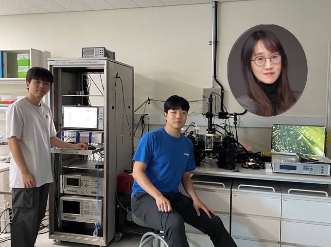 KAIST develops world’s most sensitive light-powered photodetector—20 times more sensitive, operating without electricity
<(From left) Ph.D candidate Jaeha Hwang, Ph.D candidate Jungi Song ,Professor Kayoung Lee from Electrical Engineering>
Silicon semiconductors used in existing photodetectors have low light responsivity, and the two-dimensional semiconductor MoS₂ (molybdenum disulfide) is so thin that doping processes to control its electrical properties are difficult, limiting the realization of high-performance photodetectors. The KAIST research team has overcome this technical limitation and developed the world’s highest-performing self-powered photodetector, which operates without electricity in environments with a light source. This paves the way for an era where precise sensing is possible without batteries in wearable devices, biosignal monitoring, IoT devices, autonomous vehicles, and robots, as long as a light source is present.
KAIST (President Kwang Hyung Lee) announced on the 14th of August that Professor Kayoung Lee’s research team from the School of Electrical Engineering has developed a self-powered photodetector that operates without external power supply. This sensor demonstrated a sensitivity up to 20 times higher than existing products, marking the highest performance level among comparable technologies reported to date.
Professor Kayoung Lee’s team fabricated a “PN junction structure” photodetector capable of generating electrical signals on its own in environments with light, even without an electrical energy supply, by introducing a “van der Waals bottom electrode” that makes semiconductors extremely sensitive to electrical signals without doping.
First, a “PN junction” is a structure formed by joining p-type (hole-rich) and n-type (electron-rich) materials in a semiconductor. This structure causes current to flow in one direction when exposed to light, making it a key component in photodetectors and solar cells.
Normally, to create a proper PN junction, a process called “doping” is required, which involves deliberately introducing impurities into the semiconductor to alter its electrical properties. However, two-dimensional semiconductors such as MoS₂ are only a few atoms thick, so doping in the conventional way can damage the structure or reduce performance, making it difficult to create an ideal PN junction.
To overcome these limitations and maximize device performance, the research team designed a new device structure incorporating two key technologies: the “van der Waals electrode” and the “partial gate.”
The “partial gate” structure applies an electrical signal only to part of the two-dimensional semiconductor, controlling one side to behave like p-type and the other like n-type. This allows the device to function electrically like a PN junction without doping.
Furthermore, considering that conventional metal electrodes can chemically bond strongly to the semiconductor and damage its lattice structure, the “van der Waals bottom electrode” was attached gently using van der Waals forces. This preserved the original structure of the two-dimensional semiconductor while ensuring effective electrical signal transfer.
This innovative approach secured both structural stability and electrical performance, enabling the realization of a PN junction in thin two-dimensional semiconductors without damaging their structure.
Thanks to this innovation, the team succeeded in implementing a high-performance PN junction without doping. The device can generate electrical signals with extreme sensitivity as long as there is light, even without an external power source. Its light detection sensitivity (responsivity) exceeds 21 A/W, more than 20 times higher than powered conventional sensors, 10 times higher than silicon-based self-powered sensors, and over twice as high as existing MoS₂ sensors. This level of sensitivity means it can be applied immediately to high-precision sensors capable of detecting biosignals or operating in dark environments.
Professor Kayoung Lee stated that they “have achieved a level of sensitivity unimaginable in silicon sensors, and although two-dimensional semiconductors are too thin for conventional doping processes, [they] succeeded in implementing a PN junction that controls electrical flow without doping.” She added, “This technology can be used not only in sensors but also in key components that control electricity inside smartphones and electronic devices, providing a foundation for miniaturization and self-powered operation of next-generation electronics.”
Jaeha Hwang, Jungi Song, Experimnet in Porgress>
This research, with doctoral students Jaeha Hwang and Jungi Song as co-first authors, was published online on July 26 in Advanced Functional Materials (IF 19), a leading journal in materials science.
※ Paper title: Gated PN Junction in Ambipolar MoS₂ for Superior Self-Powered Photodetection
※ DOI: https://advanced.onlinelibrary.wiley.com/doi/10.1002/adfm.202510113
Meanwhile, this work was supported by the National Research Foundation of Korea, the Korea Basic Science Institute, Samsung Electronics, and the Korea Institute for Advancement of Technology.
2025.08.16 View 3869
KAIST develops world’s most sensitive light-powered photodetector—20 times more sensitive, operating without electricity
<(From left) Ph.D candidate Jaeha Hwang, Ph.D candidate Jungi Song ,Professor Kayoung Lee from Electrical Engineering>
Silicon semiconductors used in existing photodetectors have low light responsivity, and the two-dimensional semiconductor MoS₂ (molybdenum disulfide) is so thin that doping processes to control its electrical properties are difficult, limiting the realization of high-performance photodetectors. The KAIST research team has overcome this technical limitation and developed the world’s highest-performing self-powered photodetector, which operates without electricity in environments with a light source. This paves the way for an era where precise sensing is possible without batteries in wearable devices, biosignal monitoring, IoT devices, autonomous vehicles, and robots, as long as a light source is present.
KAIST (President Kwang Hyung Lee) announced on the 14th of August that Professor Kayoung Lee’s research team from the School of Electrical Engineering has developed a self-powered photodetector that operates without external power supply. This sensor demonstrated a sensitivity up to 20 times higher than existing products, marking the highest performance level among comparable technologies reported to date.
Professor Kayoung Lee’s team fabricated a “PN junction structure” photodetector capable of generating electrical signals on its own in environments with light, even without an electrical energy supply, by introducing a “van der Waals bottom electrode” that makes semiconductors extremely sensitive to electrical signals without doping.
First, a “PN junction” is a structure formed by joining p-type (hole-rich) and n-type (electron-rich) materials in a semiconductor. This structure causes current to flow in one direction when exposed to light, making it a key component in photodetectors and solar cells.
Normally, to create a proper PN junction, a process called “doping” is required, which involves deliberately introducing impurities into the semiconductor to alter its electrical properties. However, two-dimensional semiconductors such as MoS₂ are only a few atoms thick, so doping in the conventional way can damage the structure or reduce performance, making it difficult to create an ideal PN junction.
To overcome these limitations and maximize device performance, the research team designed a new device structure incorporating two key technologies: the “van der Waals electrode” and the “partial gate.”
The “partial gate” structure applies an electrical signal only to part of the two-dimensional semiconductor, controlling one side to behave like p-type and the other like n-type. This allows the device to function electrically like a PN junction without doping.
Furthermore, considering that conventional metal electrodes can chemically bond strongly to the semiconductor and damage its lattice structure, the “van der Waals bottom electrode” was attached gently using van der Waals forces. This preserved the original structure of the two-dimensional semiconductor while ensuring effective electrical signal transfer.
This innovative approach secured both structural stability and electrical performance, enabling the realization of a PN junction in thin two-dimensional semiconductors without damaging their structure.
Thanks to this innovation, the team succeeded in implementing a high-performance PN junction without doping. The device can generate electrical signals with extreme sensitivity as long as there is light, even without an external power source. Its light detection sensitivity (responsivity) exceeds 21 A/W, more than 20 times higher than powered conventional sensors, 10 times higher than silicon-based self-powered sensors, and over twice as high as existing MoS₂ sensors. This level of sensitivity means it can be applied immediately to high-precision sensors capable of detecting biosignals or operating in dark environments.
Professor Kayoung Lee stated that they “have achieved a level of sensitivity unimaginable in silicon sensors, and although two-dimensional semiconductors are too thin for conventional doping processes, [they] succeeded in implementing a PN junction that controls electrical flow without doping.” She added, “This technology can be used not only in sensors but also in key components that control electricity inside smartphones and electronic devices, providing a foundation for miniaturization and self-powered operation of next-generation electronics.”
Jaeha Hwang, Jungi Song, Experimnet in Porgress>
This research, with doctoral students Jaeha Hwang and Jungi Song as co-first authors, was published online on July 26 in Advanced Functional Materials (IF 19), a leading journal in materials science.
※ Paper title: Gated PN Junction in Ambipolar MoS₂ for Superior Self-Powered Photodetection
※ DOI: https://advanced.onlinelibrary.wiley.com/doi/10.1002/adfm.202510113
Meanwhile, this work was supported by the National Research Foundation of Korea, the Korea Basic Science Institute, Samsung Electronics, and the Korea Institute for Advancement of Technology.
2025.08.16 View 3869 -
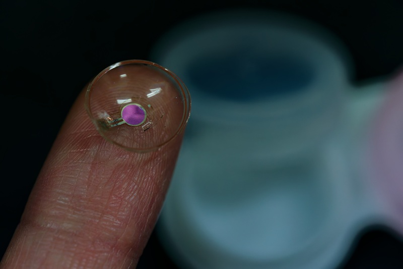 KAIST Develops World’s First Wireless OLED Contact Lens for Retinal Diagnostics
<ID-style photograph against a laboratory background featuring an OLED contact lens sample (center), flanked by the principal authors (left: Professor Seunghyup Yoo ; right: Dr. Jee Hoon Sim). Above them (from top to bottom) are: Professor Se Joon Woo, Professor Sei Kwang Hahn, Dr. Su-Bon Kim, and Dr. Hyeonwook Chae>
Electroretinography (ERG) is an ophthalmic diagnostic method used to determine whether the retina is functioning normally. It is widely employed for diagnosing hereditary retinal diseases or assessing retinal function decline.
A team of Korean researchers has developed a next-generation wireless ophthalmic diagnostic technology that replaces the existing stationary, darkroom-based retinal testing method by incorporating an “ultrathin OLED” into a contact lens. This breakthrough is expected to have applications in diverse fields such as myopia treatment, ocular biosignal analysis, augmented-reality (AR) visual information delivery, and light-based neurostimulation.
On the 12th, KAIST (President Kwang Hyung Lee) announced that a research team led by Professor Seunghyup Yoo from the School of Electrical Engineering, in collaboration with Professor Se Joon Woo of Seoul National University Bundang Hospital (Director Jeong-Han Song), Professor Sei Kwang Hahn of POSTECH (President Sung-Keun Kim) and CEO of PHI Biomed Co., and the Electronics and Telecommunications Research Institute (ETRI, President Seungchan Bang) under the National Research Council of Science & Technology (NST, Chairman Youngshik Kim), has developed the world’s first wireless contact lens-based wearable retinal diagnostic platform using organic light-emitting diodes (OLEDs).
<Figure 1. Schematic and photograph of the wireless OLED contact lens>
This technology enables ERG simply by wearing the lens, eliminating the need for large specialized light sources and dramatically simplifying the conventional, complex ophthalmic diagnostic environment.
Traditionally, ERG requires the use of a stationary Ganzfeld device in a dark room, where patients must keep their eyes open and remain still during the test. This setup imposes spatial constraints and can lead to patient fatigue and compliances challenges.
To overcome these limitations, the joint research team integrated an ultrathin flexible OLED —approximately 12.5 μm thick, or 6–8 times thinner than a human hair— into a contact lens electrode for ERG. They also equipped it with a wireless power receiving antenna and a control chip, completing a system capable of independent operation.
For power transmission, the team adopted a wireless power transfer method using a 433 MHz resonant frequency suitable for stable wireless communication. This was also demonstrated in the form of a wireless controller embedded in a sleep mask, which can be linked to a smartphone —further enhancing practical usability.
<Figure 2. Schematic of the electroretinography (ERG) testing system using a wireless OLED contact lens and an example of an actual test in progress>
While most smart contact lens–type light sources developed for ocular illumination have used inorganic LEDs, these rigid devices emit light almost from a single point, which can lead to excessive heat accumulation and thus usable light intensity. In contrast, OLEDs are areal light sources and were shown to induce retinal responses even under low luminance conditions. In this study, under a relatively low luminance* of 126 nits, the OLED contact lens successfully induced stable ERG signals, producing diagnostic results equivalent to those obtained with existing commercial light sources.
*Luminance: A value indicating how brightly a surface or screen emits light; for reference, the luminance of a smartphone screen is about 300–600 nits (can exceed 1000 nits at maximum).
Animal tests confirmed that the surface temperature of a rabbit’s eye wearing the OLED contact lens remained below 27°C, avoiding corneal heat damage, and that the light-emitting performance was maintained even in humid environments—demonstrating its effectiveness and safety as an ERG diagnostic tool in real clinical settings.
Professor Seunghyup Yoo stated that “integrating the flexibility and diffusive light characteristics of ultrathin OLEDs into a contact lens is a world-first attempt,” and that “this research can help expand smart contact lens technology into on-eye optical diagnostic and phototherapeutic platforms, contributing to the advancement of digital healthcare technology.”
< Wireless operation of the OLED contact lens >
Jee Hoon Sim, Hyeonwook Chae, and Su-Bon Kim, PhD researchers at KAIST, played a key role as co-first authors alongside Dr. Sangbaie Shin of PHI Biomed Co.. Corresponding authors are Professor Seunghyup Yoo (School of Electrical Engineering, KAIST), Professor Sei Kwang Hahn (Department of Materials Science and Engineering, POSTECH), and Professor Se Joon Woo (Seoul National University Bundang Hospital). The results were published online in the internationally renowned journal ACS Nano on May 1st.
● Paper title: Wireless Organic Light-Emitting Diode Contact Lenses for On-Eye Wearable Light Sources and Their Application to Personalized Health Monitoring
● DOI: https://doi.org/10.1021/acsnano.4c18563
● Related video clip: http://bit.ly/3UGg6R8
< Close-up of the OLED contact lens sample >
2025.08.12 View 5331
KAIST Develops World’s First Wireless OLED Contact Lens for Retinal Diagnostics
<ID-style photograph against a laboratory background featuring an OLED contact lens sample (center), flanked by the principal authors (left: Professor Seunghyup Yoo ; right: Dr. Jee Hoon Sim). Above them (from top to bottom) are: Professor Se Joon Woo, Professor Sei Kwang Hahn, Dr. Su-Bon Kim, and Dr. Hyeonwook Chae>
Electroretinography (ERG) is an ophthalmic diagnostic method used to determine whether the retina is functioning normally. It is widely employed for diagnosing hereditary retinal diseases or assessing retinal function decline.
A team of Korean researchers has developed a next-generation wireless ophthalmic diagnostic technology that replaces the existing stationary, darkroom-based retinal testing method by incorporating an “ultrathin OLED” into a contact lens. This breakthrough is expected to have applications in diverse fields such as myopia treatment, ocular biosignal analysis, augmented-reality (AR) visual information delivery, and light-based neurostimulation.
On the 12th, KAIST (President Kwang Hyung Lee) announced that a research team led by Professor Seunghyup Yoo from the School of Electrical Engineering, in collaboration with Professor Se Joon Woo of Seoul National University Bundang Hospital (Director Jeong-Han Song), Professor Sei Kwang Hahn of POSTECH (President Sung-Keun Kim) and CEO of PHI Biomed Co., and the Electronics and Telecommunications Research Institute (ETRI, President Seungchan Bang) under the National Research Council of Science & Technology (NST, Chairman Youngshik Kim), has developed the world’s first wireless contact lens-based wearable retinal diagnostic platform using organic light-emitting diodes (OLEDs).
<Figure 1. Schematic and photograph of the wireless OLED contact lens>
This technology enables ERG simply by wearing the lens, eliminating the need for large specialized light sources and dramatically simplifying the conventional, complex ophthalmic diagnostic environment.
Traditionally, ERG requires the use of a stationary Ganzfeld device in a dark room, where patients must keep their eyes open and remain still during the test. This setup imposes spatial constraints and can lead to patient fatigue and compliances challenges.
To overcome these limitations, the joint research team integrated an ultrathin flexible OLED —approximately 12.5 μm thick, or 6–8 times thinner than a human hair— into a contact lens electrode for ERG. They also equipped it with a wireless power receiving antenna and a control chip, completing a system capable of independent operation.
For power transmission, the team adopted a wireless power transfer method using a 433 MHz resonant frequency suitable for stable wireless communication. This was also demonstrated in the form of a wireless controller embedded in a sleep mask, which can be linked to a smartphone —further enhancing practical usability.
<Figure 2. Schematic of the electroretinography (ERG) testing system using a wireless OLED contact lens and an example of an actual test in progress>
While most smart contact lens–type light sources developed for ocular illumination have used inorganic LEDs, these rigid devices emit light almost from a single point, which can lead to excessive heat accumulation and thus usable light intensity. In contrast, OLEDs are areal light sources and were shown to induce retinal responses even under low luminance conditions. In this study, under a relatively low luminance* of 126 nits, the OLED contact lens successfully induced stable ERG signals, producing diagnostic results equivalent to those obtained with existing commercial light sources.
*Luminance: A value indicating how brightly a surface or screen emits light; for reference, the luminance of a smartphone screen is about 300–600 nits (can exceed 1000 nits at maximum).
Animal tests confirmed that the surface temperature of a rabbit’s eye wearing the OLED contact lens remained below 27°C, avoiding corneal heat damage, and that the light-emitting performance was maintained even in humid environments—demonstrating its effectiveness and safety as an ERG diagnostic tool in real clinical settings.
Professor Seunghyup Yoo stated that “integrating the flexibility and diffusive light characteristics of ultrathin OLEDs into a contact lens is a world-first attempt,” and that “this research can help expand smart contact lens technology into on-eye optical diagnostic and phototherapeutic platforms, contributing to the advancement of digital healthcare technology.”
< Wireless operation of the OLED contact lens >
Jee Hoon Sim, Hyeonwook Chae, and Su-Bon Kim, PhD researchers at KAIST, played a key role as co-first authors alongside Dr. Sangbaie Shin of PHI Biomed Co.. Corresponding authors are Professor Seunghyup Yoo (School of Electrical Engineering, KAIST), Professor Sei Kwang Hahn (Department of Materials Science and Engineering, POSTECH), and Professor Se Joon Woo (Seoul National University Bundang Hospital). The results were published online in the internationally renowned journal ACS Nano on May 1st.
● Paper title: Wireless Organic Light-Emitting Diode Contact Lenses for On-Eye Wearable Light Sources and Their Application to Personalized Health Monitoring
● DOI: https://doi.org/10.1021/acsnano.4c18563
● Related video clip: http://bit.ly/3UGg6R8
< Close-up of the OLED contact lens sample >
2025.08.12 View 5331 -
 Key Figures in the Establishment of KAIST, Specially Invited to the Presidential Office’s National Appointment Ceremony
KAIST announced on August 6 that Professor Emeritus Jung-Woong Ra from the Department of Electrical Engineering and Won-ki Kwon, former Vice Minister of the Ministry of Science and Technology, who played pivotal roles in the establishment of KAIST, were selected as special guests for the 'National Appointment Ceremony' hosted by the Presidential Office on August 15th.
The Presidential Office selected special invitees across eight categories for the ceremony. These include individuals born in 1945 (referred to as 'Liberation Babies'), those involved in the founding of KAIST in 1971, independence activists and national patriots, overseas workers in Germany and the Middle East, AI industry professionals, residents from regions facing depopulation, leading figures in K-culture, military personnel, firefighters, police officers, families of fallen public servants and victims of social disasters, as well as promising talents in economics, science, culture, and the arts.
Considering the historical significance of its establishment and its symbolic meaning for the development of national science and technology, KAIST Professor Emeritus Jung-Woong Ra, who was a key figure in the establishment of the Department of Electrical Engineering after being appointed as a professor in 1971, and former Vice Minister Kwon Won-ki, who was the first practical leader of the establishment project. Both were officially included on the special invitation list.
Briefing from the Presidential Office regarding the 'National Appointment Ceremony' (2025.07.28) https://www.president.go.kr/newsroom/briefing/grehGMuP
2025.08.06 View 3837
Key Figures in the Establishment of KAIST, Specially Invited to the Presidential Office’s National Appointment Ceremony
KAIST announced on August 6 that Professor Emeritus Jung-Woong Ra from the Department of Electrical Engineering and Won-ki Kwon, former Vice Minister of the Ministry of Science and Technology, who played pivotal roles in the establishment of KAIST, were selected as special guests for the 'National Appointment Ceremony' hosted by the Presidential Office on August 15th.
The Presidential Office selected special invitees across eight categories for the ceremony. These include individuals born in 1945 (referred to as 'Liberation Babies'), those involved in the founding of KAIST in 1971, independence activists and national patriots, overseas workers in Germany and the Middle East, AI industry professionals, residents from regions facing depopulation, leading figures in K-culture, military personnel, firefighters, police officers, families of fallen public servants and victims of social disasters, as well as promising talents in economics, science, culture, and the arts.
Considering the historical significance of its establishment and its symbolic meaning for the development of national science and technology, KAIST Professor Emeritus Jung-Woong Ra, who was a key figure in the establishment of the Department of Electrical Engineering after being appointed as a professor in 1971, and former Vice Minister Kwon Won-ki, who was the first practical leader of the establishment project. Both were officially included on the special invitation list.
Briefing from the Presidential Office regarding the 'National Appointment Ceremony' (2025.07.28) https://www.president.go.kr/newsroom/briefing/grehGMuP
2025.08.06 View 3837 -
 Is 24-hour health monitoring possible with ambient light energy?
<(From left) Ph.D candidate Youngmin Sim, Ph.D candidate Do Yun Park, Dr. Chanho Park, Professor Kyeongha Kwon>
Miniaturization and weight reduction of medical wearable devices for continuous health monitoring such as heart rate, blood oxygen saturation, and sweat component analysis remain major challenges. In particular, optical sensors consume a significant amount of power for LED operation and wireless transmission, requiring heavy and bulky batteries. To overcome these limitations, KAIST researchers have developed a next-generation wearable platform that enables 24-hour continuous measurement by using ambient light as an energy source and optimizing power management according to the power environment.
KAIST (President Kwang Hyung Lee) announced on the 30th that Professor Kyeongha Kwon's team from the School of Electrical Engineering, in collaboration with Dr. Chanho Park’s team at Northwestern University in the U.S., has developed an adaptive wireless wearable platform that reduces battery load by utilizing ambient light.
To address the battery issue of medical wearable devices, Professor Kyeongha Kwon’s research team developed an innovative platform that utilizes ambient natural light as an energy source. This platform integrates three complementary light energy technologies.
<Figure1.The wireless wearable platform minimizes the energy required for light sources through i) Photometric system that directly utilizes ambient light passing through windows for measurements, ii) Photovoltaic system that receives power from high-efficiency photovoltaic cells and wireless power receiver coils, and iii) Photoluminescent system that stores light using photoluminescent materials and emits light in dark conditions to support the two aforementioned systems. In-sensor computing minimizes power consumption by wirelessly transmitting only essential data. The adaptive power management system efficiently manages power by automatically selecting the optimal mode among 11 different power modes through a power selector based on the power supply level from the photovoltaic system and battery charge status.>
The first core technology, the Photometric Method, is a technique that adaptively adjusts LED brightness depending on the intensity of the ambient light source. By combining ambient natural light with LED light to maintain a constant total illumination level, it automatically dims the LED when natural light is strong and brightens it when natural light is weak.
Whereas conventional sensors had to keep the LED on at a fixed brightness regardless of the environment, this technology optimizes LED power in real time according to the surrounding environment. Experimental results showed that it reduced power consumption by as much as 86.22% under sufficient lighting conditions.
The second is the Photovoltaic Method using high-efficiency multijunction solar cells. This goes beyond simple solar power generation to convert light in both indoor and outdoor environments into electricity. In particular, the adaptive power management system automatically switches among 11 different power configurations based on ambient conditions and battery status to achieve optimal energy efficiency.
The third innovative technology is the Photoluminescent Method. By mixing strontium aluminate microparticles* into the sensor’s silicone encapsulation structure, light from the surroundings is absorbed and stored during the day and slowly released in the dark. As a result, after being exposed to 500W/m² of sunlight for 10 minutes, continuous measurement is possible for 2.5 minutes even in complete darkness.
*Strontium aluminate microparticles: A photoluminescent material used in glow-in-the-dark paint or safety signs, which absorbs light and emits it in the dark for an extended time.
These three technologies work complementarily—during bright conditions, the first and second methods are active, and in dark conditions, the third method provides additional support—enabling 24-hour continuous operation.
The research team applied this platform to various medical sensors to verify its practicality. The photoplethysmography sensor monitors heart rate and blood oxygen saturation in real time, allowing early detection of cardiovascular diseases. The blue light dosimeter accurately measures blue light, which causes skin aging and damage, and provides personalized skin protection guidance. The sweat analysis sensor uses microfluidic technology to simultaneously analyze salt, glucose, and pH in sweat, enabling real-time detection of dehydration and electrolyte imbalances.
Additionally, introducing in-sensor data computing significantly reduced wireless communication power consumption. Previously, all raw data had to be transmitted externally, but now only the necessary results are calculated and transmitted within the sensor, reducing data transmission requirements from 400B/s to 4B/s—a 100-fold decrease.
To validate performance, the research tested the device on healthy adult subjects in four different environments: bright indoor lighting, dim lighting, infrared lighting, and complete darkness. The results showed measurement accuracy equivalent to that of commercial medical devices in all conditions A mouse model experiment confirmed accurate blood oxygen saturation measurement in hypoxic conditions.
<Frigure2.The multimodal device applying the energy harvesting and power management platform consists of i) photoplethysmography (PPG) sensor, ii) blue light dosimeter, iii) photoluminescent microfluidic channel for sweat analysis and biomarker sensors (chloride ion, glucose, and pH), and iv) temperature sensor. This device was implemented with flexible printed circuit board (fPCB) to enable attachment to the skin. A silicon substrate with a window that allows ambient light and measurement light to pass through, along with photoluminescent encapsulation layer, encapsulates the PPG, blue light dosimeter, and temperature sensors, while the photoluminescent microfluidic channel is attached below the photoluminescent encapsulation layer to collect sweat>
Professor Kyeongha Kwon of KAIST, who led the research, stated, “This technology will enable 24-hour continuous health monitoring, shifting the medical paradigm from treatment-centered to prevention-centered shifting the medical paradigm from treatment-centered to prevention-centered,” further stating that “cost savings through early diagnosis as well as strengthened technological competitiveness in the next-generation wearable healthcare market are anticipated.”
This research was published on July 1 in the international journal Nature Communications, with Do Yun Park, a doctoral student in the AI Semiconductor Graduate Program, as co–first author.
※ Paper title: Adaptive Electronics for Photovoltaic, Photoluminescent and Photometric Methods in Power Harvesting for Wireless and Wearable Sensors ※ DOI: https://doi.org/10.1038/s41467-025-60911-1 ※ URL: https://www.nature.com/articles/s41467-025-60911-1
This research was supported by the National Research Foundation of Korea (Outstanding Young Researcher Program and Regional Innovation Leading Research Center Project), the Ministry of Science and ICT and Institute of Information & Communications Technology Planning & Evaluation (IITP) AI Semiconductor Graduate Program, and the BK FOUR Program (Connected AI Education & Research Program for Industry and Society Innovation, KAIST EE).
2025.07.30 View 4843
Is 24-hour health monitoring possible with ambient light energy?
<(From left) Ph.D candidate Youngmin Sim, Ph.D candidate Do Yun Park, Dr. Chanho Park, Professor Kyeongha Kwon>
Miniaturization and weight reduction of medical wearable devices for continuous health monitoring such as heart rate, blood oxygen saturation, and sweat component analysis remain major challenges. In particular, optical sensors consume a significant amount of power for LED operation and wireless transmission, requiring heavy and bulky batteries. To overcome these limitations, KAIST researchers have developed a next-generation wearable platform that enables 24-hour continuous measurement by using ambient light as an energy source and optimizing power management according to the power environment.
KAIST (President Kwang Hyung Lee) announced on the 30th that Professor Kyeongha Kwon's team from the School of Electrical Engineering, in collaboration with Dr. Chanho Park’s team at Northwestern University in the U.S., has developed an adaptive wireless wearable platform that reduces battery load by utilizing ambient light.
To address the battery issue of medical wearable devices, Professor Kyeongha Kwon’s research team developed an innovative platform that utilizes ambient natural light as an energy source. This platform integrates three complementary light energy technologies.
<Figure1.The wireless wearable platform minimizes the energy required for light sources through i) Photometric system that directly utilizes ambient light passing through windows for measurements, ii) Photovoltaic system that receives power from high-efficiency photovoltaic cells and wireless power receiver coils, and iii) Photoluminescent system that stores light using photoluminescent materials and emits light in dark conditions to support the two aforementioned systems. In-sensor computing minimizes power consumption by wirelessly transmitting only essential data. The adaptive power management system efficiently manages power by automatically selecting the optimal mode among 11 different power modes through a power selector based on the power supply level from the photovoltaic system and battery charge status.>
The first core technology, the Photometric Method, is a technique that adaptively adjusts LED brightness depending on the intensity of the ambient light source. By combining ambient natural light with LED light to maintain a constant total illumination level, it automatically dims the LED when natural light is strong and brightens it when natural light is weak.
Whereas conventional sensors had to keep the LED on at a fixed brightness regardless of the environment, this technology optimizes LED power in real time according to the surrounding environment. Experimental results showed that it reduced power consumption by as much as 86.22% under sufficient lighting conditions.
The second is the Photovoltaic Method using high-efficiency multijunction solar cells. This goes beyond simple solar power generation to convert light in both indoor and outdoor environments into electricity. In particular, the adaptive power management system automatically switches among 11 different power configurations based on ambient conditions and battery status to achieve optimal energy efficiency.
The third innovative technology is the Photoluminescent Method. By mixing strontium aluminate microparticles* into the sensor’s silicone encapsulation structure, light from the surroundings is absorbed and stored during the day and slowly released in the dark. As a result, after being exposed to 500W/m² of sunlight for 10 minutes, continuous measurement is possible for 2.5 minutes even in complete darkness.
*Strontium aluminate microparticles: A photoluminescent material used in glow-in-the-dark paint or safety signs, which absorbs light and emits it in the dark for an extended time.
These three technologies work complementarily—during bright conditions, the first and second methods are active, and in dark conditions, the third method provides additional support—enabling 24-hour continuous operation.
The research team applied this platform to various medical sensors to verify its practicality. The photoplethysmography sensor monitors heart rate and blood oxygen saturation in real time, allowing early detection of cardiovascular diseases. The blue light dosimeter accurately measures blue light, which causes skin aging and damage, and provides personalized skin protection guidance. The sweat analysis sensor uses microfluidic technology to simultaneously analyze salt, glucose, and pH in sweat, enabling real-time detection of dehydration and electrolyte imbalances.
Additionally, introducing in-sensor data computing significantly reduced wireless communication power consumption. Previously, all raw data had to be transmitted externally, but now only the necessary results are calculated and transmitted within the sensor, reducing data transmission requirements from 400B/s to 4B/s—a 100-fold decrease.
To validate performance, the research tested the device on healthy adult subjects in four different environments: bright indoor lighting, dim lighting, infrared lighting, and complete darkness. The results showed measurement accuracy equivalent to that of commercial medical devices in all conditions A mouse model experiment confirmed accurate blood oxygen saturation measurement in hypoxic conditions.
<Frigure2.The multimodal device applying the energy harvesting and power management platform consists of i) photoplethysmography (PPG) sensor, ii) blue light dosimeter, iii) photoluminescent microfluidic channel for sweat analysis and biomarker sensors (chloride ion, glucose, and pH), and iv) temperature sensor. This device was implemented with flexible printed circuit board (fPCB) to enable attachment to the skin. A silicon substrate with a window that allows ambient light and measurement light to pass through, along with photoluminescent encapsulation layer, encapsulates the PPG, blue light dosimeter, and temperature sensors, while the photoluminescent microfluidic channel is attached below the photoluminescent encapsulation layer to collect sweat>
Professor Kyeongha Kwon of KAIST, who led the research, stated, “This technology will enable 24-hour continuous health monitoring, shifting the medical paradigm from treatment-centered to prevention-centered shifting the medical paradigm from treatment-centered to prevention-centered,” further stating that “cost savings through early diagnosis as well as strengthened technological competitiveness in the next-generation wearable healthcare market are anticipated.”
This research was published on July 1 in the international journal Nature Communications, with Do Yun Park, a doctoral student in the AI Semiconductor Graduate Program, as co–first author.
※ Paper title: Adaptive Electronics for Photovoltaic, Photoluminescent and Photometric Methods in Power Harvesting for Wireless and Wearable Sensors ※ DOI: https://doi.org/10.1038/s41467-025-60911-1 ※ URL: https://www.nature.com/articles/s41467-025-60911-1
This research was supported by the National Research Foundation of Korea (Outstanding Young Researcher Program and Regional Innovation Leading Research Center Project), the Ministry of Science and ICT and Institute of Information & Communications Technology Planning & Evaluation (IITP) AI Semiconductor Graduate Program, and the BK FOUR Program (Connected AI Education & Research Program for Industry and Society Innovation, KAIST EE).
2025.07.30 View 4843 -
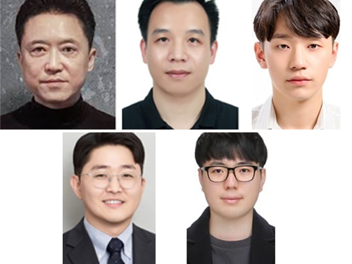 Vulnerability Found: One Packet Can Paralyze Smartphones
<(From left) Professor Yongdae Kim, PhD candidate Tuan Dinh Hoang, PhD candidate Taekkyung Oh from KAIST, Professor CheolJun Park from Kyung Hee University; and Professor Insu Yun from KAIST>
Smartphones must stay connected to mobile networks at all times to function properly. The core component that enables this constant connectivity is the communication modem (Baseband) inside the device. KAIST researchers, using their self-developed testing framework called 'LLFuzz (Lower Layer Fuzz),' have discovered security vulnerabilities in the lower layers of smartphone communication modems and demonstrated the necessity of standardizing 'mobile communication modem security testing.'
*Standardization: In mobile communication, conformance testing, which verifies normal operation in normal situations, has been standardized. However, standards for handling abnormal packets have not yet been established, hence the need for standardized security testing.
Professor Yongdae Kim's team from the School of Electrical Engineering at KAIST, in a joint research effort with Professor CheolJun Park's team from Kyung Hee University, announced on the 25th of July that they have discovered critical security vulnerabilities in the lower layers of smartphone communication modems. These vulnerabilities can incapacitate smartphone communication with just a single manipulated wireless packet (a data transmission unit in a network). In particular, these vulnerabilities are extremely severe as they can potentially lead to remote code execution (RCE)
The research team utilized their self-developed 'LLFuzz' analysis framework to analyze the lower layer state transitions and error handling logic of the modem to detect security vulnerabilities. LLFuzz was able to precisely extract vulnerabilities caused by implementation errors by comparing and analyzing 3GPP* standard-based state machines with actual device responses.
*3GPP: An international collaborative organization that creates global mobile communication standards.
The research team conducted experiments on 15 commercial smartphones from global manufacturers, including Apple, Samsung Electronics, Google, and Xiaomi, and discovered a total of 11 vulnerabilities. Among these, seven were assigned official CVE (Common Vulnerabilities and Exposures) numbers, and manufacturers applied security patches for these vulnerabilities. However, the remaining four have not yet been publicly disclosed.
While previous security research primarily focused on higher layers of mobile communication, such as NAS (Network Access Stratum) and RRC (Radio Resource Control), the research team concentrated on analyzing the error handling logic of mobile communication's lower layers, which manufacturers have often neglected.
These vulnerabilities occurred in the lower layers of the communication modem (RLC, MAC, PDCP, PHY*), and due to their structural characteristics where encryption or authentication is not applied, operational errors could be induced simply by injecting external signals.
*RLC, MAC, PDCP, PHY: Lower layers of LTE/5G communication, responsible for wireless resource allocation, error control, encryption, and physical layer transmission.
The research team released a demo video showing that when they injected a manipulated wireless packet (malformed MAC packet) into commercial smartphones via a Software-Defined Radio (SDR) device using packets generated on an experimental laptop, the smartphone's communication modem (Baseband) immediately crashed
※ Experiment video: https://drive.google.com/file/d/1NOwZdu_Hf4ScG7LkwgEkHLa_nSV4FPb_/view?usp=drive_link
The video shows data being normally transmitted at 23MB per second on the fast.com page, but immediately after the manipulated packet is injected, the transmission stops and the mobile communication signal disappears. This intuitively demonstrates that a single wireless packet can cripple a commercial device's communication modem.
The vulnerabilities were found in the 'modem chip,' a core component of smartphones responsible for calls, texts, and data communication, making it a very important component.
Qualcomm: Affects over 90 chipsets, including CVE-2025-21477, CVE-2024-23385.
MediaTek: Affects over 80 chipsets, including CVE-2024-20076, CVE-2024-20077, CVE-2025-20659.
Samsung: CVE-2025-26780 (targets the latest chipsets like Exynos 2400, 5400).
Apple: CVE-2024-27870 (shares the same vulnerability as Qualcomm CVE).
The problematic modem chips (communication components) are not only in premium smartphones but also in low-end smartphones, tablets, smartwatches, and IoT devices, leading to the widespread potential for user harm due to their broad diffusion.
Furthermore, the research team experimentally tested 5G vulnerabilities in the lower layers and found two vulnerabilities in just two weeks. Considering that 5G vulnerability checks have not been generally conducted, it is possible that many more vulnerabilities exist in the mobile communication lower layers of baseband chips.
Professor Yongdae Kim explained, "The lower layers of smartphone communication modems are not subject to encryption or authentication, creating a structural risk where devices can accept arbitrary signals from external sources." He added, "This research demonstrates the necessity of standardizing mobile communication modem security testing for smartphones and other IoT devices."
The research team is continuing additional analysis of the 5G lower layers using LLFuzz and is also developing tools for testing LTE and 5G upper layers. They are also pursuing collaborations for future tool disclosure. The team's stance is that "as technological complexity increases, systemic security inspection systems must evolve in parallel."
First author Tuan Dinh Hoang, a Ph.D. student in the School of Electrical Engineering, will present the research results in August at USENIX Security 2025, one of the world's most prestigious conferences in cybersecurity.
※ Paper Title: LLFuzz: An Over-the-Air Dynamic Testing Framework for Cellular Baseband Lower Layers (Tuan Dinh Hoang and Taekkyung Oh, KAIST; CheolJun Park, Kyung Hee Univ.; Insu Yun and Yongdae Kim, KAIST)
※ Usenix paper site: https://www.usenix.org/conference/usenixsecurity25/presentation/hoang (Not yet public), Lab homepage paper: https://syssec.kaist.ac.kr/pub/2025/LLFuzz_Tuan.pdf
※ Open-source repository: https://github.com/SysSec-KAIST/LLFuzz (To be released)
This research was conducted with support from the Institute of Information & Communications Technology Planning & Evaluation (IITP) funded by the Ministry of Science and ICT.
2025.07.25 View 4769
Vulnerability Found: One Packet Can Paralyze Smartphones
<(From left) Professor Yongdae Kim, PhD candidate Tuan Dinh Hoang, PhD candidate Taekkyung Oh from KAIST, Professor CheolJun Park from Kyung Hee University; and Professor Insu Yun from KAIST>
Smartphones must stay connected to mobile networks at all times to function properly. The core component that enables this constant connectivity is the communication modem (Baseband) inside the device. KAIST researchers, using their self-developed testing framework called 'LLFuzz (Lower Layer Fuzz),' have discovered security vulnerabilities in the lower layers of smartphone communication modems and demonstrated the necessity of standardizing 'mobile communication modem security testing.'
*Standardization: In mobile communication, conformance testing, which verifies normal operation in normal situations, has been standardized. However, standards for handling abnormal packets have not yet been established, hence the need for standardized security testing.
Professor Yongdae Kim's team from the School of Electrical Engineering at KAIST, in a joint research effort with Professor CheolJun Park's team from Kyung Hee University, announced on the 25th of July that they have discovered critical security vulnerabilities in the lower layers of smartphone communication modems. These vulnerabilities can incapacitate smartphone communication with just a single manipulated wireless packet (a data transmission unit in a network). In particular, these vulnerabilities are extremely severe as they can potentially lead to remote code execution (RCE)
The research team utilized their self-developed 'LLFuzz' analysis framework to analyze the lower layer state transitions and error handling logic of the modem to detect security vulnerabilities. LLFuzz was able to precisely extract vulnerabilities caused by implementation errors by comparing and analyzing 3GPP* standard-based state machines with actual device responses.
*3GPP: An international collaborative organization that creates global mobile communication standards.
The research team conducted experiments on 15 commercial smartphones from global manufacturers, including Apple, Samsung Electronics, Google, and Xiaomi, and discovered a total of 11 vulnerabilities. Among these, seven were assigned official CVE (Common Vulnerabilities and Exposures) numbers, and manufacturers applied security patches for these vulnerabilities. However, the remaining four have not yet been publicly disclosed.
While previous security research primarily focused on higher layers of mobile communication, such as NAS (Network Access Stratum) and RRC (Radio Resource Control), the research team concentrated on analyzing the error handling logic of mobile communication's lower layers, which manufacturers have often neglected.
These vulnerabilities occurred in the lower layers of the communication modem (RLC, MAC, PDCP, PHY*), and due to their structural characteristics where encryption or authentication is not applied, operational errors could be induced simply by injecting external signals.
*RLC, MAC, PDCP, PHY: Lower layers of LTE/5G communication, responsible for wireless resource allocation, error control, encryption, and physical layer transmission.
The research team released a demo video showing that when they injected a manipulated wireless packet (malformed MAC packet) into commercial smartphones via a Software-Defined Radio (SDR) device using packets generated on an experimental laptop, the smartphone's communication modem (Baseband) immediately crashed
※ Experiment video: https://drive.google.com/file/d/1NOwZdu_Hf4ScG7LkwgEkHLa_nSV4FPb_/view?usp=drive_link
The video shows data being normally transmitted at 23MB per second on the fast.com page, but immediately after the manipulated packet is injected, the transmission stops and the mobile communication signal disappears. This intuitively demonstrates that a single wireless packet can cripple a commercial device's communication modem.
The vulnerabilities were found in the 'modem chip,' a core component of smartphones responsible for calls, texts, and data communication, making it a very important component.
Qualcomm: Affects over 90 chipsets, including CVE-2025-21477, CVE-2024-23385.
MediaTek: Affects over 80 chipsets, including CVE-2024-20076, CVE-2024-20077, CVE-2025-20659.
Samsung: CVE-2025-26780 (targets the latest chipsets like Exynos 2400, 5400).
Apple: CVE-2024-27870 (shares the same vulnerability as Qualcomm CVE).
The problematic modem chips (communication components) are not only in premium smartphones but also in low-end smartphones, tablets, smartwatches, and IoT devices, leading to the widespread potential for user harm due to their broad diffusion.
Furthermore, the research team experimentally tested 5G vulnerabilities in the lower layers and found two vulnerabilities in just two weeks. Considering that 5G vulnerability checks have not been generally conducted, it is possible that many more vulnerabilities exist in the mobile communication lower layers of baseband chips.
Professor Yongdae Kim explained, "The lower layers of smartphone communication modems are not subject to encryption or authentication, creating a structural risk where devices can accept arbitrary signals from external sources." He added, "This research demonstrates the necessity of standardizing mobile communication modem security testing for smartphones and other IoT devices."
The research team is continuing additional analysis of the 5G lower layers using LLFuzz and is also developing tools for testing LTE and 5G upper layers. They are also pursuing collaborations for future tool disclosure. The team's stance is that "as technological complexity increases, systemic security inspection systems must evolve in parallel."
First author Tuan Dinh Hoang, a Ph.D. student in the School of Electrical Engineering, will present the research results in August at USENIX Security 2025, one of the world's most prestigious conferences in cybersecurity.
※ Paper Title: LLFuzz: An Over-the-Air Dynamic Testing Framework for Cellular Baseband Lower Layers (Tuan Dinh Hoang and Taekkyung Oh, KAIST; CheolJun Park, Kyung Hee Univ.; Insu Yun and Yongdae Kim, KAIST)
※ Usenix paper site: https://www.usenix.org/conference/usenixsecurity25/presentation/hoang (Not yet public), Lab homepage paper: https://syssec.kaist.ac.kr/pub/2025/LLFuzz_Tuan.pdf
※ Open-source repository: https://github.com/SysSec-KAIST/LLFuzz (To be released)
This research was conducted with support from the Institute of Information & Communications Technology Planning & Evaluation (IITP) funded by the Ministry of Science and ICT.
2025.07.25 View 4769 -
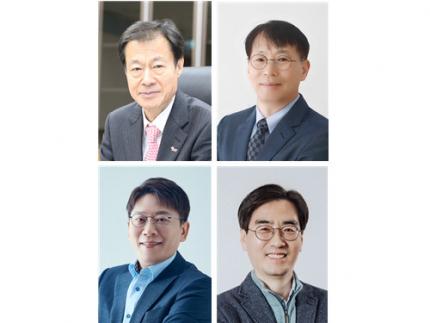 KAIST Alumni Association to Honor Alumni of the Year Award Winners
Photo 1. Photo of the KAIST Alumni of the Year Award Recipients
(From left) UST President Lee-whan Kim, CEO Han Chung of iThree Systems Co., Ltd., CEO Dong Myung Kim of LG Energy Solution Co., Ltd., and Professor Hyun Myung of the School of Electrical Engineering at KAIST
KAIST (President Kwang Hyung Lee) announced on Monday, the 13th of January that the Alumni Association (President Yun-Tae Lee) has selected its Alumni of the Year.
This year’s honorees are: ▴ President Lee-whan Kim of the Korea National University of Science and Technology (UST), ▴ CEO Han Chung of i3 Systems, ▴ CEO Dong Myung Kim of LG Energy Solution, and ▴ Professor Hyun Myung of the School of Electrical Engineering at KAIST.
The honorees were selected based on their achievements over the past year, and the award ceremony will be held at the 2025 KAIST Alumni Association New Year’s Gathering to be held at the L Tower in Seoul at 5 PM on Friday the 17th.
The KAIST Alumni of the Year Award is an award presented by the Alumni Association to alumni who have contributed to the development of the country and the society or have brought honor to their alma mater through outstanding academic achievements and community service. Since its establishment in 1992, 126 recipients have been awarded.
Lee-whan Kim (Master's graduate of Mechanical Engineering, 82), the President of the Korea National University of Science and Technology (UST), established a leading foundation for national science and technology policy and strategy, and played a leading role in innovating national science and technology capabilities through the advancement of the national research and development system and the advancement of science and technology personnel training. In particular, he played a pivotal role in the establishment of UST and the Korea Science Academy (KSA), and greatly contributed to establishing a foundation for the training and utilization of science and technology personnel.
Han Chung (Master's graduate of Electrical Engineering, 91, with Ph.D. degree in 96), the CEO of i3 Systems, is a first-generation researcher in the field of domestic infrared detectors. He developed military detectors for over 30 years and founded i3 Systems, a specialized infrared detector company, in 1998. Currently, he supplies more than 80% of the infrared detectors used by the Korean military, and has also achieved export results to over 20 countries.
Dong Myung Kim (Master's graduate of Materials Science and Engineering, 94, with Ph.D. degree in 98) the CEO of LG Energy Solution Co., Ltd. has led innovation in the battery field with his ceaseless exploration and challenging spirit, and is known as an authority in the secondary battery industry. He played a leading role in establishing K-Battery as a global leader, strengthened the country's future industrial competitiveness, and greatly contributed to the development of science and technology.
Hyun Myung (Bachelor's graduate of Electrical Engineering, 92, with Master's degree in 94, and Ph.D. degree in 98) a Professor of Electrical Engineering, KAIST, won first place in the world at the Quadruped Robot Challenge (QRC) hosted by the IEEE’s International Conference on Robotics and Automation (ICRA) 2023 with the 'DreamWaQ' system, an AI walking technology based on deep reinforcement learning that utilizes non-video sensory technologies. He contributed to enhancing the competitiveness of the domestic robot industry by developing his own fully autonomous walking technology that recognizes the environment around the robot and finds the optimal path.
Yun-Tae Lee, the 27th president of the KAIST Alumni Association, said, “KAIST alumni have been the driving force behind the growth of industries in all walks of life by continuously conducting research and development in the field of advanced science and technology for a long time,” and added, “I am very proud of the KAIST alumni award recipients who are leading science and technology on the world stage beyond Korea, and I sincerely thank them for their efforts and achievements.”
2025.01.15 View 13527
KAIST Alumni Association to Honor Alumni of the Year Award Winners
Photo 1. Photo of the KAIST Alumni of the Year Award Recipients
(From left) UST President Lee-whan Kim, CEO Han Chung of iThree Systems Co., Ltd., CEO Dong Myung Kim of LG Energy Solution Co., Ltd., and Professor Hyun Myung of the School of Electrical Engineering at KAIST
KAIST (President Kwang Hyung Lee) announced on Monday, the 13th of January that the Alumni Association (President Yun-Tae Lee) has selected its Alumni of the Year.
This year’s honorees are: ▴ President Lee-whan Kim of the Korea National University of Science and Technology (UST), ▴ CEO Han Chung of i3 Systems, ▴ CEO Dong Myung Kim of LG Energy Solution, and ▴ Professor Hyun Myung of the School of Electrical Engineering at KAIST.
The honorees were selected based on their achievements over the past year, and the award ceremony will be held at the 2025 KAIST Alumni Association New Year’s Gathering to be held at the L Tower in Seoul at 5 PM on Friday the 17th.
The KAIST Alumni of the Year Award is an award presented by the Alumni Association to alumni who have contributed to the development of the country and the society or have brought honor to their alma mater through outstanding academic achievements and community service. Since its establishment in 1992, 126 recipients have been awarded.
Lee-whan Kim (Master's graduate of Mechanical Engineering, 82), the President of the Korea National University of Science and Technology (UST), established a leading foundation for national science and technology policy and strategy, and played a leading role in innovating national science and technology capabilities through the advancement of the national research and development system and the advancement of science and technology personnel training. In particular, he played a pivotal role in the establishment of UST and the Korea Science Academy (KSA), and greatly contributed to establishing a foundation for the training and utilization of science and technology personnel.
Han Chung (Master's graduate of Electrical Engineering, 91, with Ph.D. degree in 96), the CEO of i3 Systems, is a first-generation researcher in the field of domestic infrared detectors. He developed military detectors for over 30 years and founded i3 Systems, a specialized infrared detector company, in 1998. Currently, he supplies more than 80% of the infrared detectors used by the Korean military, and has also achieved export results to over 20 countries.
Dong Myung Kim (Master's graduate of Materials Science and Engineering, 94, with Ph.D. degree in 98) the CEO of LG Energy Solution Co., Ltd. has led innovation in the battery field with his ceaseless exploration and challenging spirit, and is known as an authority in the secondary battery industry. He played a leading role in establishing K-Battery as a global leader, strengthened the country's future industrial competitiveness, and greatly contributed to the development of science and technology.
Hyun Myung (Bachelor's graduate of Electrical Engineering, 92, with Master's degree in 94, and Ph.D. degree in 98) a Professor of Electrical Engineering, KAIST, won first place in the world at the Quadruped Robot Challenge (QRC) hosted by the IEEE’s International Conference on Robotics and Automation (ICRA) 2023 with the 'DreamWaQ' system, an AI walking technology based on deep reinforcement learning that utilizes non-video sensory technologies. He contributed to enhancing the competitiveness of the domestic robot industry by developing his own fully autonomous walking technology that recognizes the environment around the robot and finds the optimal path.
Yun-Tae Lee, the 27th president of the KAIST Alumni Association, said, “KAIST alumni have been the driving force behind the growth of industries in all walks of life by continuously conducting research and development in the field of advanced science and technology for a long time,” and added, “I am very proud of the KAIST alumni award recipients who are leading science and technology on the world stage beyond Korea, and I sincerely thank them for their efforts and achievements.”
2025.01.15 View 13527 -
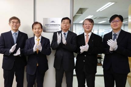 “Cross-Generation Collaborative Labs” for Semiconductor, Chemistry, and Computer Science Opened
< Photo of Professor Hoi-Jun Yoo (center) of the School of Electrical Engineering at the signboard unveiling ceremony >
KAIST held a ceremony to mark the opening of three additional ‘Cross-Generation Collaborative Labs’ on the morning of January 7th, 2025.
The “Next-Generation AI Semiconductor System Lab” by Professor Hoi-Jun Yoo of the School of Electrical Engineering, the “Molecular Spectroscopy and Chemical Dynamics Lab” by Professor Sang Kyu Kim of the Department of Chemistry, and the “Advanced Data Computing Lab” by Professor Sue Bok Moon of the School of Computer Science are the three new labs given the honored titled of the “Cross-Generation Collaborative Lab”.
The Cross-Generation Collaborative Lab is KAIST’s unique system that was set up to facilitate the collaboration between retiring professors and junior professors to continue the achievements and know-how the elders have accumulated over their academic career. Since its introduction in 2018, nine labs have been named to be the Cross-Generation Labs, and this year’s new addition brings the total up to twelve.
The ‘Next-Generation AI Semiconductor System Lab’ led by Professor Hoi-Jun Yoo will be operated by Professor Joo-Young Kim of the same school.
Professor Hoi-Jun Yoo is a world-renowned scholar with outstanding research achievements in the field of on-device AI semiconductor design. Professor Joo-Young Kim is an up-and-coming researcher studying large language models and design of AI semiconductors for server computers, and is currently researching technologies to design PIM (Processing-in-Memory), a core technology in the field of AI semiconductors.
Their research goal is to systematically collaborate and transfer next-generation AI semiconductor design technology, including brain-mimicking AI algorithms such as deep neural networks and generative AI, to integrate core technologies, and to maximize the usability of R&D outputs, thereby further solidifying the position of Korean AI semiconductor companies in the global market.
Professor Hoi-Jun Yoo said, “I believe that, we will be able to present a development direction of for the next-generation AI semiconductors industries at home and abroad through collaborative research and play a key role in transferring and expanding global leadership.”
< Professor Sang Kyu Kim of the Department of Chemistry (middle), at the signboard unveiling ceremony for his laboratory >
The “Molecular Spectroscopy and Chemical Dynamics Laboratory”, where Professor Sang Kyu Kim of the Department of Chemistry is in charge, will be operated by Professor Tae Kyu Kim of the same department, and another professor in the field of spectroscopy and dynamics will join in the future.
Professor Sang Kyu Kim has secured technologies for developing unique experimental equipment based on ultrashort lasers and supersonic molecular beams, and is a world leader who has been creatively pioneering new fields of experimental physical chemistry.
The research goal is to describe chemical reactions and verify from a quantum mechanical perspective and introduce new theories and technologies to pursue a complete understanding of the principles of chemical reactions. In addition, the accompanying basic scientific knowledge will be applied to the design of new materials.
Professor Sang Kyu Kim said, “I am very happy to be able to pass on the research infrastructure to the next generation through this system, and I will continue to nurture it to grow into a world-class research lab through trans-generational collaborative research.”
< Photo of Professor Sue Bok Moon (center) at the signboard unveiling ceremony by the School of Computing >
Lastly, the “Advanced Data Computing Lab” led by Professor Sue Bok Moon is joined by Professor Mee Young Cha of the same school and Professor Wonjae Lee of the Graduate School of Culture Technology.
Professor Sue Bok Moon showed the infinite possibilities of large-scale data-based social network research through Cyworld, YouTube, and Twitter, and had a great influence on related fields beyond the field of computer science.
Professor Mee Young Cha is a data scientist who analyzes difficult social issues such as misinformation, poverty, and disaster detection using big data-based AI. She is the first Korean to be recognized for her achievements as the director of the Max Planck Institute in Germany, a world-class basic science research institute. Therefore, there is high expectation for synergy effects from overseas collaborative research and technology transfer and sharing among the participating professors of the collaborative research lab. Professor Wonjae Lee is researching dynamic interaction analysis between science and technology using structural topic models.
They plan to conduct research aimed at improving the analysis and understanding of negative influences occurring online, and in particular, developing a hateful precursor detection model using emotions and morality to preemptively block hateful expressions.
Professor Sue Bok Moon said, “Through this collaborative research lab, we will play a key role in conducting in-depth collaborative research on unexpected negative influences in the AI era so that we can have a high level of competitiveness worldwide.”
The ceremonies for the unveiling of the new Cross-Generation Collaborative Lab signboard were held in front of each lab from 10:00 AM on the 7th, in the attendance of President Kwang Hyung Lee, Senior Vice President for Research Sang Yup Lee, and other key officials of KAIST and the new staff members to join the laboratories.
2025.01.07 View 12535
“Cross-Generation Collaborative Labs” for Semiconductor, Chemistry, and Computer Science Opened
< Photo of Professor Hoi-Jun Yoo (center) of the School of Electrical Engineering at the signboard unveiling ceremony >
KAIST held a ceremony to mark the opening of three additional ‘Cross-Generation Collaborative Labs’ on the morning of January 7th, 2025.
The “Next-Generation AI Semiconductor System Lab” by Professor Hoi-Jun Yoo of the School of Electrical Engineering, the “Molecular Spectroscopy and Chemical Dynamics Lab” by Professor Sang Kyu Kim of the Department of Chemistry, and the “Advanced Data Computing Lab” by Professor Sue Bok Moon of the School of Computer Science are the three new labs given the honored titled of the “Cross-Generation Collaborative Lab”.
The Cross-Generation Collaborative Lab is KAIST’s unique system that was set up to facilitate the collaboration between retiring professors and junior professors to continue the achievements and know-how the elders have accumulated over their academic career. Since its introduction in 2018, nine labs have been named to be the Cross-Generation Labs, and this year’s new addition brings the total up to twelve.
The ‘Next-Generation AI Semiconductor System Lab’ led by Professor Hoi-Jun Yoo will be operated by Professor Joo-Young Kim of the same school.
Professor Hoi-Jun Yoo is a world-renowned scholar with outstanding research achievements in the field of on-device AI semiconductor design. Professor Joo-Young Kim is an up-and-coming researcher studying large language models and design of AI semiconductors for server computers, and is currently researching technologies to design PIM (Processing-in-Memory), a core technology in the field of AI semiconductors.
Their research goal is to systematically collaborate and transfer next-generation AI semiconductor design technology, including brain-mimicking AI algorithms such as deep neural networks and generative AI, to integrate core technologies, and to maximize the usability of R&D outputs, thereby further solidifying the position of Korean AI semiconductor companies in the global market.
Professor Hoi-Jun Yoo said, “I believe that, we will be able to present a development direction of for the next-generation AI semiconductors industries at home and abroad through collaborative research and play a key role in transferring and expanding global leadership.”
< Professor Sang Kyu Kim of the Department of Chemistry (middle), at the signboard unveiling ceremony for his laboratory >
The “Molecular Spectroscopy and Chemical Dynamics Laboratory”, where Professor Sang Kyu Kim of the Department of Chemistry is in charge, will be operated by Professor Tae Kyu Kim of the same department, and another professor in the field of spectroscopy and dynamics will join in the future.
Professor Sang Kyu Kim has secured technologies for developing unique experimental equipment based on ultrashort lasers and supersonic molecular beams, and is a world leader who has been creatively pioneering new fields of experimental physical chemistry.
The research goal is to describe chemical reactions and verify from a quantum mechanical perspective and introduce new theories and technologies to pursue a complete understanding of the principles of chemical reactions. In addition, the accompanying basic scientific knowledge will be applied to the design of new materials.
Professor Sang Kyu Kim said, “I am very happy to be able to pass on the research infrastructure to the next generation through this system, and I will continue to nurture it to grow into a world-class research lab through trans-generational collaborative research.”
< Photo of Professor Sue Bok Moon (center) at the signboard unveiling ceremony by the School of Computing >
Lastly, the “Advanced Data Computing Lab” led by Professor Sue Bok Moon is joined by Professor Mee Young Cha of the same school and Professor Wonjae Lee of the Graduate School of Culture Technology.
Professor Sue Bok Moon showed the infinite possibilities of large-scale data-based social network research through Cyworld, YouTube, and Twitter, and had a great influence on related fields beyond the field of computer science.
Professor Mee Young Cha is a data scientist who analyzes difficult social issues such as misinformation, poverty, and disaster detection using big data-based AI. She is the first Korean to be recognized for her achievements as the director of the Max Planck Institute in Germany, a world-class basic science research institute. Therefore, there is high expectation for synergy effects from overseas collaborative research and technology transfer and sharing among the participating professors of the collaborative research lab. Professor Wonjae Lee is researching dynamic interaction analysis between science and technology using structural topic models.
They plan to conduct research aimed at improving the analysis and understanding of negative influences occurring online, and in particular, developing a hateful precursor detection model using emotions and morality to preemptively block hateful expressions.
Professor Sue Bok Moon said, “Through this collaborative research lab, we will play a key role in conducting in-depth collaborative research on unexpected negative influences in the AI era so that we can have a high level of competitiveness worldwide.”
The ceremonies for the unveiling of the new Cross-Generation Collaborative Lab signboard were held in front of each lab from 10:00 AM on the 7th, in the attendance of President Kwang Hyung Lee, Senior Vice President for Research Sang Yup Lee, and other key officials of KAIST and the new staff members to join the laboratories.
2025.01.07 View 12535