Applied+Physics
-
 Press Release on Piezoelectric Nanogenerators of ZnO with Aluminium Nitride Stacked Layers by the American Institute of Physics
The
American Institute of Physics (AIP) released a news article entitled “Zinc
Oxide Materials Tapped for Tiny Energy Harvesting Devices” on January 13, 2015.
The
article described the research led by Professor Giwan Yoon of the
Electrical Engineering Department at KAIST. It was published in the January
12, 2015 issue of Applied Physics Letters.
AIP publishes the journal. For the news release, please visit the
link below:
The American
Institute of Physics, January 13, 2015
“Zinc
Oxide Materials Tapped for Tiny Energy Harvesting Devices”
New research helps
pave the way toward highly energy-efficient zinc oxide-based micro energy
harvesting devices with applications in portable communications, healthcare and
environmental monitoring, and more
http://www.aip.org/publishing/journal-highlights/zinc-oxide-materials-tapped-tiny-energy-harvesting-devices
2015.02.04 View 34472
 -
 Newsweek: The Goosebump Sensor That Knows How You Feel
Newsweek covered the introduction of the goosebump sensor invented by Professor Young-Ho Cho of the Department of Bio and Brain Engineering at KAIST in an article dated July 27, 2014.
The article entitled “The Goosebump Sensor That Knows How You Feel” explains how the sensor works and reports on the current research and development trends in emotion-sensing technology.
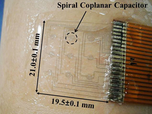
Professor Cho’s research paper was originally published in the journal Applied Physics Letters on June 24, 2014, titled “A Flexible Skin Piloerection Monitoring Sensor."
Newsweek, July 27, 2014
“The Goosebump Sensor That Knows How You Feel”
http://www.newsweek.com/goosebump-sensor-knows-how-you-feel-260689
2014.07.28 View 9349
 -
 Prof. Choi Unveils Method to Improve Emission Efficiency of OLED
A KAIST research team led by Prof. Kyung-Cheol Choi of the School of Electrical Engineering & Computer Science discovered the surface plasmon-enhanced spontaneous emission based on an organic light-emitting device (OLED), a finding expected to improve OLED"s emission efficiency, KAIST authorities said on Thursday (July 9).
For surface plasmon localization, silver nanoparticles were thermally deposited in a high vacuum on cathode. Since plasmons provide a strong oscillator decay channel, time-resolved photoluninescene (PL) results displayed a 1.75-fold increased emission rate, and continuous wave PL results showed a twofold enhanced intensity.
"The method using surface plasmon represents a new technology to enhance the emission efficiency of OLED. It is expected to greatly contribute to the development of new technologies in OLED and flexible display, as well as securing original technology," Prof. Choi said.
The finding was published in the April issue of Applied Physics Letters and the June 25 issue of Optics Express. It will be also featured as the research highlight of the August issue of Nature Photonics and Virtual Journal of Ultrafast Science.
2009.07.09 View 23091
 -
 KAIST Scientists Creates Transparent Memory Chip
--See-Through Semis Could Revolutionize Displays
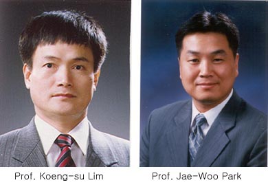
A group of KAIST scientists led by Prof. Jae-Woo Park and Koeng-Su Lim has created a working computer chip that is almost completely clear -- the first of its kind.
The new chip, called "transparent resistive random access memory (TRRAM), is similar in type to an existing technology known as complementary metal-oxide semiconductor (CMOS) memory -- common commercial chips that provide the data storage for USB flash drives and other devices. Like CMOS devices, the new chip provides "non-volatile" memory, meaning that it stores digital information without losing data when it is powered off. Unlike CMOS devices, however, the new TRRAM chip is almost completely clear.
The paper on the new technology, entitled "Transparent resistive random access memory and its characteristics for non-volatile resistive switching," was published in the December issue of the Applied Physics Letters (APL), and the American Institute of Physics, the publisher of APL, issued a press release about this breakthrough.
"It is a new milestone of transparent electronic systems," says researcher Jung-Won Seo, who is the first author of the paper. "By integrating TRRAM devices with other transparent electronic components, we can create a totally see-through embedded electronic system."
Technically, TRRAM devices rely upon an existing technology known as resistive random access memory (RRAM), which is already in commercial development for future electronic data storage devices. RRAM is built using metal oxide materials between equally transparent electrodes and substrates.
According to the research team, TRRAM devices are easy to fabricate and may be commercially available in just 3-4 years.
"We are sure that TRRAM will become one of alternative devices to current CMOS-based flash memory in the near future after its reliability is proven and once any manufacturing issues are solved," says Prof. Jae-Woo Park, who is the co-author on the paper. He adds that the new devices have the potential to be manufactured cheaply because any transparent materials can be utilized as substrate and electrode. They also may not require incorporating rare elements such as Indium.
2008.12.17 View 19442