Advanced+Optical+Materials
-
 Extracting Light from Graphite: Core Technology of Graphene Quantum Dots Display Developed
Professor Seokwoo Jeon of the Department of Materials Science and Engineering, Professor Yong-Hoon Cho of the Department of Physics, and Professor Seunghyup Yoo of the Department of Electrical Engineering announced that they were able to develop topnotch graphene quantum dots from graphite.
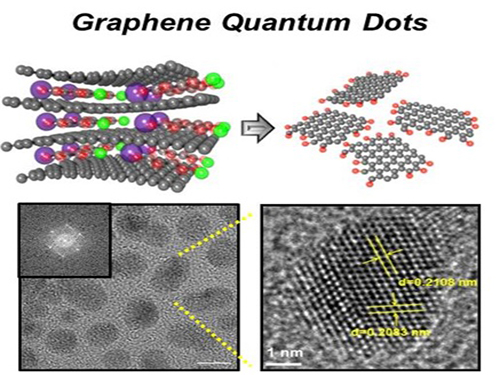
Using the method of synthesizing graphite intercalation compound from graphite with salt and water, the research team developed graphene quantum dots in an ecofriendly way.
The quantum dots have a diameter of 5 nanometers with their sizes equal and yield high quantum efficiency. Unlike conventional quantum dots, they are not comprised of toxic materials such as lead or cadmium. As the quantum dots can be developed from materials which can be easily found in the nature, researchers look forward to putting these into mass production at low cost.
The research team also discovered a luminescence mechanism of graphene quantum dots and confirmed the possibility of commercial use by developing quantum dot light-emitting diodes with brightness of 1,000 cd/m2, which is greater than that of cellphone displays.
Professor Seokwoo Jeon said, “Although quantum dot LEDs have a lower luminous efficiency than existing ones, their luminescent property can be further improved” and emphasized that “using quantum dot displays will allow us to develop not only paper-thin displays but also flexible ones.”
Sponsored by Graphene Research Center in KAIST Institute for NanoCentury, the research finding was published online in the April 20th issue of Advanced Optical Materials.
Picture 1: Graphene quantum dots and their synthesis
Picture 2: Luminescence mechanism of graphene quantum dots
Picture 3: Structure of graphene quantum dots LED and its emission
2014.09.06 View 19752
 -
 New Technology Will Enable the Commercialization of Plasmon Displays
-- Enhancements in the penetration ratios of color filters are expected by applying nano-surface plasmon effects. --
-- Color filter technology will be applicable to large-area OLED and LCD. --
The fabrication technology to commercialize display color filters using plasmon effects has been discovered.
A joint research team headed by Professor Kyung Cheol Choi from the Department of Electrical Engineering of the Korea Advanced Institute for Science and Technology and Prof. Byeong-Kwon Ju from the School of Electrical Engineering of Korea University has developed the technology to design and produce a display color filter by applying nano-surface plasmon effects.
Color filters are core components used to express colors in CMOS image sensors found in LCD/OLED displays or digital cameras. The current color filters have penetration ratios of 20~30%, but the objective of the joint research team is to raise this penetration ratio by over 40% to facilitate the mass production of energy-efficient plasmonic displays.
Currently available plasmonic color filters are limited to applications on micrometer scales. However, outcomes of the newest research extend the size of the applications up to 2.5 cm by using laser interference lithography. The academic and industrial sectors agree that it is now possible to mass-produce displays using plasmonic color filters.
The researchers built a nanohole array to large scale by using laser interference lithography, a technology that forms nanostructures with laser light interferences. They also suggested a new manufacturing process that can optimize the features of color filters while compensating for defects arising from the fabrication stages.
The new manufacturing process of applying laser interference lithography is expected to overcome the shortcomings of traditional color filters by simplifying production and, enabling them to be produced at lower costs.
“There were limitations to industrial applications of plasmon effect due to production costs, time, and yields,” explained Yun Seon Do, a Ph. D. candidate in the Department of Electrical Engineering of KAIST. “The new technology can reduce fabrication time and cost to the extent that it would be advisable to replace dye-based and pigment-based color filter technology."
“This research can be applied to large-scale displays, such as TV screens, by using laser-interference lithography,” said Jung-Ho Park, a Ph. D. candidate in the School of Electrical Engineering of Korea University. “The research outcome is expected to be widely applied in advanced nano-manufacturing processes as it does not restrict the types of circuit boards."
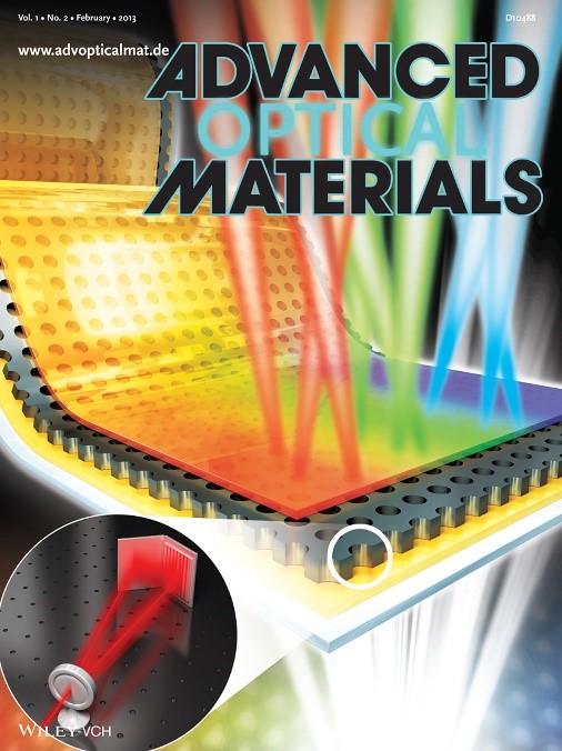
The research outcome, led by doctoral candidates Do and Park, appeared on the front cover of the second issue of Advanced Optical Materials, a highly regarded academic journal in the field of nanotechnologies, and the team has applied for six related patents.
2013.03.13 View 10018