Technology
-
 Hyung Kyu Lim, Former KAIST Alumni Association President, Donates 100 Million Won for a Challenge to Follow “I am a KAIST”
Hyung Kyu Lim, a former President of the KAIST Alumni Association, has donated 100 million won as the prize money for the School Song and National Anthem Challenge. This donation will be used as prize money starting from the 2026 competition and is expected to play a significant role in spreading KAIST's educational culture and fostering a sense of community.
< Photo 1. KAIST President Kwang-Hyung Lee (left) and the former Alumni Association President Hyung Kyu Lim at the ceremony for the signing of the pledge for Dr. Lim's donation. >
The School Song and National Anthem Challenge was first conceived in 2024 at the suggestion of President Kwang-Hyung Lee to enhance consensus on KAIST's values and educational philosophy and to inspire patriotism and school spirit. Participants express their sense of belonging and pride in KAIST by singing the KAIST school song, the national anthem, or the 'I'm a KAIST,' dedicated by Professor Sumi Jo, a visiting scholar at the Graduate School of Culture Technology. Notably, this year, a new category has been added where participants sing their self-composed 'My Own School Song,' making the stage more diverse.
The grand prize-winning team receives the President's Award and a prize of 1 million won. The top excellence award and participating teams also receive prizes and awards totaling 2 million won.
< Photo 2. At the ceremony for the signing of the donation pledge, KAIST President Kwang-Hyung Lee (left) is relaying a bouquet of flower and the plaque of appreciation to the former Alumni Association President Hyung Kyu Lim. >
Former Alumni Association President Hyung Kyu Lim stated, Love for the national community is the foundation of a sound global citizen consciousness. For me, love for this national community, along with family love, has been a great source of energy for growth.
He added, I hope this challenge of singing the national anthem and school song becomes a good nourishment for KAIST members to grow into global citizens with roots, expressing his thoughts on the donation.
President Kwang-Hyung Lee said, “I am grateful to former Alumni Association President Hyung Kyu Lim for his generous support of this meaningful program, which fosters pride in the school and raises interest in loving the country through the national anthem.” He added, “This donation will serve as an opportunity for KAIST members to cultivate a sense of belonging to the school and a sense of responsibility to the national community.”
Since 2018, former President Lim has annually donated prize money for the 'Linkgenesis Best Teacher Award,' encouraging faculty members who embody the values of creativity, challenge, and consideration. Furthermore, he has consistently contributed to KAIST's talent development and advancement by continuing to provide funds totaling 1 billion won, including scholarship funds for the Department of Electrical Engineering and the Alumni Academic Scholarship Foundation.
< Photo 3. Grand prize-winning team of the School Song and National Anthem Challenge >
Meanwhile, the '2nd School Song and National Anthem Challenge' was successfully held on May 21st at the main auditorium of KAIST, with over 150 spectators participating. Eight teams performed in the finals, and the final winning team was selected based on audience evaluation (10%) and judges' scores (90%).
< Photo 4. Grand prize-winning team of the School Song and National Anthem Challenge, Aeguk-Rock in performance >
The grand prize was awarded to the 'Aeguk-Rock' team, who arranged the national anthem into a rock version and performed it as a band. The top excellence award went to the 'Form of the Conductor' team, who sang the school song a cappella. The excellence award was given to Eun-Jin Choi, a student from the Graduate School of Culture Technology, who performed her self-composed school song written with an AI tool, 'Radiant You – You Are KAIST.' The 'Aeguk-Rock’ team also won the audience popularity award, and five other teams received participation awards.
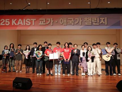
< Photo 5. Group photo of the winners of the School Song and National Anthem Challenge >
2025.05.23 View 9
Hyung Kyu Lim, Former KAIST Alumni Association President, Donates 100 Million Won for a Challenge to Follow “I am a KAIST”
Hyung Kyu Lim, a former President of the KAIST Alumni Association, has donated 100 million won as the prize money for the School Song and National Anthem Challenge. This donation will be used as prize money starting from the 2026 competition and is expected to play a significant role in spreading KAIST's educational culture and fostering a sense of community.
< Photo 1. KAIST President Kwang-Hyung Lee (left) and the former Alumni Association President Hyung Kyu Lim at the ceremony for the signing of the pledge for Dr. Lim's donation. >
The School Song and National Anthem Challenge was first conceived in 2024 at the suggestion of President Kwang-Hyung Lee to enhance consensus on KAIST's values and educational philosophy and to inspire patriotism and school spirit. Participants express their sense of belonging and pride in KAIST by singing the KAIST school song, the national anthem, or the 'I'm a KAIST,' dedicated by Professor Sumi Jo, a visiting scholar at the Graduate School of Culture Technology. Notably, this year, a new category has been added where participants sing their self-composed 'My Own School Song,' making the stage more diverse.
The grand prize-winning team receives the President's Award and a prize of 1 million won. The top excellence award and participating teams also receive prizes and awards totaling 2 million won.
< Photo 2. At the ceremony for the signing of the donation pledge, KAIST President Kwang-Hyung Lee (left) is relaying a bouquet of flower and the plaque of appreciation to the former Alumni Association President Hyung Kyu Lim. >
Former Alumni Association President Hyung Kyu Lim stated, Love for the national community is the foundation of a sound global citizen consciousness. For me, love for this national community, along with family love, has been a great source of energy for growth.
He added, I hope this challenge of singing the national anthem and school song becomes a good nourishment for KAIST members to grow into global citizens with roots, expressing his thoughts on the donation.
President Kwang-Hyung Lee said, “I am grateful to former Alumni Association President Hyung Kyu Lim for his generous support of this meaningful program, which fosters pride in the school and raises interest in loving the country through the national anthem.” He added, “This donation will serve as an opportunity for KAIST members to cultivate a sense of belonging to the school and a sense of responsibility to the national community.”
Since 2018, former President Lim has annually donated prize money for the 'Linkgenesis Best Teacher Award,' encouraging faculty members who embody the values of creativity, challenge, and consideration. Furthermore, he has consistently contributed to KAIST's talent development and advancement by continuing to provide funds totaling 1 billion won, including scholarship funds for the Department of Electrical Engineering and the Alumni Academic Scholarship Foundation.
< Photo 3. Grand prize-winning team of the School Song and National Anthem Challenge >
Meanwhile, the '2nd School Song and National Anthem Challenge' was successfully held on May 21st at the main auditorium of KAIST, with over 150 spectators participating. Eight teams performed in the finals, and the final winning team was selected based on audience evaluation (10%) and judges' scores (90%).
< Photo 4. Grand prize-winning team of the School Song and National Anthem Challenge, Aeguk-Rock in performance >
The grand prize was awarded to the 'Aeguk-Rock' team, who arranged the national anthem into a rock version and performed it as a band. The top excellence award went to the 'Form of the Conductor' team, who sang the school song a cappella. The excellence award was given to Eun-Jin Choi, a student from the Graduate School of Culture Technology, who performed her self-composed school song written with an AI tool, 'Radiant You – You Are KAIST.' The 'Aeguk-Rock’ team also won the audience popularity award, and five other teams received participation awards.
< Photo 5. Group photo of the winners of the School Song and National Anthem Challenge >
2025.05.23 View 9 -
 2025 National Strategic Technology Innovation Forum Held - Seeking ROK-U.S. Cooperation
The Future Institute for National Strategic Technology and Policy (FINST&P) at KAIST will host the 'National Strategic Technology* Innovation Forum for 1st half of 2025' on Thursday, May 22, at the Chung Kunmo Conference Hall in the Academic and Culture Building (E9) at the KAIST Main Campus in Daejeon.
* National Strategic Technologies: Technologies recognized for their strategic importance in terms of diplomacy and security, with significant impact on the national economy and related industries, and serving as the foundation for future innovation, including the creation of new technologies and industries. Currently, 12 major technologies such as AI, advanced bio, quantum, and semiconductors, and 50 detailed key technologies are being selected and supported (「Special Act on Fostering National Strategic Technologies」).
This forum will examine the policy direction for fostering national strategic technologies in South Korea amidst rapidly changing international dynamics, such as escalating conflict between the United States and China and increasing global security uncertainties. Furthermore, it will discuss ways to strengthen technology innovation between South Korea and the United States to secure scientific and technological sovereignty and future growth engines.
The forum will feature: △An opening address by KAIST President Kwang-Hyung Lee △Congratulatory remarks by Minister Sang-im Yoo of the Ministry of Science and ICT △A keynote speech by Robert D. Atkinson, President of the Information Technology and Innovation Foundation (ITIF) of the U.S. Subsequently, △Part 1, ‘ROK-U.S. Science and Technology Cooperation,’ will share the latest global trends in national strategic technologies and discuss ROK-U.S. science and technology cooperation under the U.S.-China technology hegemony structure.
Following this, △Part 2, ‘ROK-U.S. Cooperation in Key Detailed Technology Fields,’ will analyze R&D trends and current issues focusing on major national strategic technologies, and derive action-oriented policy tasks that South Korea can pursue based on ROK-U.S. cooperation.
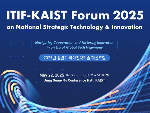
< National Strategic Technology Innovation Forum Poster >
Each session of Part 1 and Part 2 will consist of presentations by domestic and international experts, followed by a comprehensive discussion and Q&A with the audience, promising more in-depth discussions.
Robert D. Atkinson, President of the U.S. Information Technology and Innovation Foundation (ITIF), in his keynote speech ‘The Trump 2.0 Era: South Korea's New Growth Strategy,’ suggests that South Korea should shift from its existing export-oriented growth to a new growth strategy based on broad technological innovation, and promote technological innovation by improving "shadow regulations" imposed by social practices.
The first presenter in Part 1, Stephen Ezell, Vice President for Global Innovation Policy at ITIF, emphasizes in ‘U.S.-China Conflict: South Korea's Response and Global Implications’ that South Korea must overcome the crisis by improving overall national productivity and fostering a competitive service industry.
Following this, Kyungjin Song, Country Representative of The Asia Foundation Korea Office, suggests in ‘Strengthening ROK-U.S. Strategic Technology Partnership Cooperation’ that as global technological hegemony competition changes the diplomatic and security landscape, ROK-U.S. cooperation should advance towards an institutional and sustainable cooperation foundation through a multi-layered partnership structure involving both countries' parliaments, industries, academia, and civil society.
Jaemin Jung, Dean of the College of Humanities and Social Sciences at KAIST, in ‘The Value of Humanities, Social Sciences, and Arts in the Age of Artificial Intelligence,’ explains the role and importance of the KAIST College of Humanities and Social Sciences in connecting technological innovation with human-centered values, as responsible technological development of artificial intelligence (AI) is difficult without insights into humans, society, and culture, presenting examples through AI joint research projects conducted with MIT.
As the first presenter in Part 2, Yong-hee Kim, Director of the Future Institute for National Strategic Technology and Policy (FINST&P) at KAIST, in ‘ROK-U.S. Cooperation for Truly Sustainable Next-Generation Nuclear Power,’ states that many countries or companies are pursuing nuclear power for carbon neutrality and energy security. He suggests that to achieve sustainable nuclear power, three major issues—safety, spent fuel, and uranium resources—need to be resolved, and the molten salt fast reactor (MSFR), an advanced reactor, can be an effective solution.*Molten Salt Fast Reactor (MSFR): A type of Generation IV nuclear reactor that uses molten salt as nuclear fuel and coolant in a fast neutron reactor.
Byung Hee Hong, Professor at Seoul National University's Department of Chemistry, predicts in ‘Innovation in Strategic Industries Led by Graphene Mass Production Technology’ that graphene is a ‘dream new material’ that will overcome the limitations of existing technologies. If South Korea succeeds in mass-producing graphene, it will bring tremendous innovation across key industries such as AI semiconductors and sensors, quantum computing, and biomedical.
Finally, Hoi-Jun Yoo, Distinguished Professor at the KAIST Graduate School of Artificial Intelligence Semiconductor, in ‘The Present and Future of AI Semiconductors,’ explains that with the full-scale utilization of large-scale AI like ChatGPT, semiconductor design is tending to reorganize from a computation-centric to a memory-centric approach. He then presents the direction and feasibility of mid-to-long-term strategies for the competitive development of Korean AI semiconductors.
KAIST President Kwang-Hyung Lee stated the purpose of the event, saying, "As national strategic technology is a core agenda directly linked to our nation's future growth, KAIST will continue to provide a platform for science and technology and policy to communicate, together with domestic and international industry-academia-research institutions."
This event is co-hosted with the U.S. think tank Information Technology and Innovation Foundation (ITIF), which has played a leading role in science and technology innovation policy, with the sponsorship of the Ministry of Science and ICT.
2025.05.16 View 17
2025 National Strategic Technology Innovation Forum Held - Seeking ROK-U.S. Cooperation
The Future Institute for National Strategic Technology and Policy (FINST&P) at KAIST will host the 'National Strategic Technology* Innovation Forum for 1st half of 2025' on Thursday, May 22, at the Chung Kunmo Conference Hall in the Academic and Culture Building (E9) at the KAIST Main Campus in Daejeon.
* National Strategic Technologies: Technologies recognized for their strategic importance in terms of diplomacy and security, with significant impact on the national economy and related industries, and serving as the foundation for future innovation, including the creation of new technologies and industries. Currently, 12 major technologies such as AI, advanced bio, quantum, and semiconductors, and 50 detailed key technologies are being selected and supported (「Special Act on Fostering National Strategic Technologies」).
This forum will examine the policy direction for fostering national strategic technologies in South Korea amidst rapidly changing international dynamics, such as escalating conflict between the United States and China and increasing global security uncertainties. Furthermore, it will discuss ways to strengthen technology innovation between South Korea and the United States to secure scientific and technological sovereignty and future growth engines.
The forum will feature: △An opening address by KAIST President Kwang-Hyung Lee △Congratulatory remarks by Minister Sang-im Yoo of the Ministry of Science and ICT △A keynote speech by Robert D. Atkinson, President of the Information Technology and Innovation Foundation (ITIF) of the U.S. Subsequently, △Part 1, ‘ROK-U.S. Science and Technology Cooperation,’ will share the latest global trends in national strategic technologies and discuss ROK-U.S. science and technology cooperation under the U.S.-China technology hegemony structure.
Following this, △Part 2, ‘ROK-U.S. Cooperation in Key Detailed Technology Fields,’ will analyze R&D trends and current issues focusing on major national strategic technologies, and derive action-oriented policy tasks that South Korea can pursue based on ROK-U.S. cooperation.
< National Strategic Technology Innovation Forum Poster >
Each session of Part 1 and Part 2 will consist of presentations by domestic and international experts, followed by a comprehensive discussion and Q&A with the audience, promising more in-depth discussions.
Robert D. Atkinson, President of the U.S. Information Technology and Innovation Foundation (ITIF), in his keynote speech ‘The Trump 2.0 Era: South Korea's New Growth Strategy,’ suggests that South Korea should shift from its existing export-oriented growth to a new growth strategy based on broad technological innovation, and promote technological innovation by improving "shadow regulations" imposed by social practices.
The first presenter in Part 1, Stephen Ezell, Vice President for Global Innovation Policy at ITIF, emphasizes in ‘U.S.-China Conflict: South Korea's Response and Global Implications’ that South Korea must overcome the crisis by improving overall national productivity and fostering a competitive service industry.
Following this, Kyungjin Song, Country Representative of The Asia Foundation Korea Office, suggests in ‘Strengthening ROK-U.S. Strategic Technology Partnership Cooperation’ that as global technological hegemony competition changes the diplomatic and security landscape, ROK-U.S. cooperation should advance towards an institutional and sustainable cooperation foundation through a multi-layered partnership structure involving both countries' parliaments, industries, academia, and civil society.
Jaemin Jung, Dean of the College of Humanities and Social Sciences at KAIST, in ‘The Value of Humanities, Social Sciences, and Arts in the Age of Artificial Intelligence,’ explains the role and importance of the KAIST College of Humanities and Social Sciences in connecting technological innovation with human-centered values, as responsible technological development of artificial intelligence (AI) is difficult without insights into humans, society, and culture, presenting examples through AI joint research projects conducted with MIT.
As the first presenter in Part 2, Yong-hee Kim, Director of the Future Institute for National Strategic Technology and Policy (FINST&P) at KAIST, in ‘ROK-U.S. Cooperation for Truly Sustainable Next-Generation Nuclear Power,’ states that many countries or companies are pursuing nuclear power for carbon neutrality and energy security. He suggests that to achieve sustainable nuclear power, three major issues—safety, spent fuel, and uranium resources—need to be resolved, and the molten salt fast reactor (MSFR), an advanced reactor, can be an effective solution.*Molten Salt Fast Reactor (MSFR): A type of Generation IV nuclear reactor that uses molten salt as nuclear fuel and coolant in a fast neutron reactor.
Byung Hee Hong, Professor at Seoul National University's Department of Chemistry, predicts in ‘Innovation in Strategic Industries Led by Graphene Mass Production Technology’ that graphene is a ‘dream new material’ that will overcome the limitations of existing technologies. If South Korea succeeds in mass-producing graphene, it will bring tremendous innovation across key industries such as AI semiconductors and sensors, quantum computing, and biomedical.
Finally, Hoi-Jun Yoo, Distinguished Professor at the KAIST Graduate School of Artificial Intelligence Semiconductor, in ‘The Present and Future of AI Semiconductors,’ explains that with the full-scale utilization of large-scale AI like ChatGPT, semiconductor design is tending to reorganize from a computation-centric to a memory-centric approach. He then presents the direction and feasibility of mid-to-long-term strategies for the competitive development of Korean AI semiconductors.
KAIST President Kwang-Hyung Lee stated the purpose of the event, saying, "As national strategic technology is a core agenda directly linked to our nation's future growth, KAIST will continue to provide a platform for science and technology and policy to communicate, together with domestic and international industry-academia-research institutions."
This event is co-hosted with the U.S. think tank Information Technology and Innovation Foundation (ITIF), which has played a leading role in science and technology innovation policy, with the sponsorship of the Ministry of Science and ICT.
2025.05.16 View 17 -
 KAIST Alumni Association to Honor Alumni of the Year Award Winners
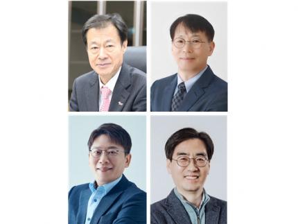
Photo 1. Photo of the KAIST Alumni of the Year Award Recipients
(From left) UST President Lee-whan Kim, CEO Han Chung of iThree Systems Co., Ltd., CEO Dong Myung Kim of LG Energy Solution Co., Ltd., and Professor Hyun Myung of the School of Electrical Engineering at KAIST
KAIST (President Kwang Hyung Lee) announced on Monday, the 13th of January that the Alumni Association (President Yun-Tae Lee) has selected its Alumni of the Year.
This year’s honorees are: ▴ President Lee-whan Kim of the Korea National University of Science and Technology (UST), ▴ CEO Han Chung of i3 Systems, ▴ CEO Dong Myung Kim of LG Energy Solution, and ▴ Professor Hyun Myung of the School of Electrical Engineering at KAIST.
The honorees were selected based on their achievements over the past year, and the award ceremony will be held at the 2025 KAIST Alumni Association New Year’s Gathering to be held at the L Tower in Seoul at 5 PM on Friday the 17th.
The KAIST Alumni of the Year Award is an award presented by the Alumni Association to alumni who have contributed to the development of the country and the society or have brought honor to their alma mater through outstanding academic achievements and community service. Since its establishment in 1992, 126 recipients have been awarded.
Lee-whan Kim (Master's graduate of Mechanical Engineering, 82), the President of the Korea National University of Science and Technology (UST), established a leading foundation for national science and technology policy and strategy, and played a leading role in innovating national science and technology capabilities through the advancement of the national research and development system and the advancement of science and technology personnel training. In particular, he played a pivotal role in the establishment of UST and the Korea Science Academy (KSA), and greatly contributed to establishing a foundation for the training and utilization of science and technology personnel.
Han Chung (Master's graduate of Electrical Engineering, 91, with Ph.D. degree in 96), the CEO of i3 Systems, is a first-generation researcher in the field of domestic infrared detectors. He developed military detectors for over 30 years and founded i3 Systems, a specialized infrared detector company, in 1998. Currently, he supplies more than 80% of the infrared detectors used by the Korean military, and has also achieved export results to over 20 countries.
Dong Myung Kim (Master's graduate of Materials Science and Engineering, 94, with Ph.D. degree in 98) the CEO of LG Energy Solution Co., Ltd. has led innovation in the battery field with his ceaseless exploration and challenging spirit, and is known as an authority in the secondary battery industry. He played a leading role in establishing K-Battery as a global leader, strengthened the country's future industrial competitiveness, and greatly contributed to the development of science and technology.
Hyun Myung (Bachelor's graduate of Electrical Engineering, 92, with Master's degree in 94, and Ph.D. degree in 98) a Professor of Electrical Engineering, KAIST, won first place in the world at the Quadruped Robot Challenge (QRC) hosted by the IEEE’s International Conference on Robotics and Automation (ICRA) 2023 with the 'DreamWaQ' system, an AI walking technology based on deep reinforcement learning that utilizes non-video sensory technologies. He contributed to enhancing the competitiveness of the domestic robot industry by developing his own fully autonomous walking technology that recognizes the environment around the robot and finds the optimal path.
Yun-Tae Lee, the 27th president of the KAIST Alumni Association, said, “KAIST alumni have been the driving force behind the growth of industries in all walks of life by continuously conducting research and development in the field of advanced science and technology for a long time,” and added, “I am very proud of the KAIST alumni award recipients who are leading science and technology on the world stage beyond Korea, and I sincerely thank them for their efforts and achievements.”
2025.01.15 View 3259
KAIST Alumni Association to Honor Alumni of the Year Award Winners
Photo 1. Photo of the KAIST Alumni of the Year Award Recipients
(From left) UST President Lee-whan Kim, CEO Han Chung of iThree Systems Co., Ltd., CEO Dong Myung Kim of LG Energy Solution Co., Ltd., and Professor Hyun Myung of the School of Electrical Engineering at KAIST
KAIST (President Kwang Hyung Lee) announced on Monday, the 13th of January that the Alumni Association (President Yun-Tae Lee) has selected its Alumni of the Year.
This year’s honorees are: ▴ President Lee-whan Kim of the Korea National University of Science and Technology (UST), ▴ CEO Han Chung of i3 Systems, ▴ CEO Dong Myung Kim of LG Energy Solution, and ▴ Professor Hyun Myung of the School of Electrical Engineering at KAIST.
The honorees were selected based on their achievements over the past year, and the award ceremony will be held at the 2025 KAIST Alumni Association New Year’s Gathering to be held at the L Tower in Seoul at 5 PM on Friday the 17th.
The KAIST Alumni of the Year Award is an award presented by the Alumni Association to alumni who have contributed to the development of the country and the society or have brought honor to their alma mater through outstanding academic achievements and community service. Since its establishment in 1992, 126 recipients have been awarded.
Lee-whan Kim (Master's graduate of Mechanical Engineering, 82), the President of the Korea National University of Science and Technology (UST), established a leading foundation for national science and technology policy and strategy, and played a leading role in innovating national science and technology capabilities through the advancement of the national research and development system and the advancement of science and technology personnel training. In particular, he played a pivotal role in the establishment of UST and the Korea Science Academy (KSA), and greatly contributed to establishing a foundation for the training and utilization of science and technology personnel.
Han Chung (Master's graduate of Electrical Engineering, 91, with Ph.D. degree in 96), the CEO of i3 Systems, is a first-generation researcher in the field of domestic infrared detectors. He developed military detectors for over 30 years and founded i3 Systems, a specialized infrared detector company, in 1998. Currently, he supplies more than 80% of the infrared detectors used by the Korean military, and has also achieved export results to over 20 countries.
Dong Myung Kim (Master's graduate of Materials Science and Engineering, 94, with Ph.D. degree in 98) the CEO of LG Energy Solution Co., Ltd. has led innovation in the battery field with his ceaseless exploration and challenging spirit, and is known as an authority in the secondary battery industry. He played a leading role in establishing K-Battery as a global leader, strengthened the country's future industrial competitiveness, and greatly contributed to the development of science and technology.
Hyun Myung (Bachelor's graduate of Electrical Engineering, 92, with Master's degree in 94, and Ph.D. degree in 98) a Professor of Electrical Engineering, KAIST, won first place in the world at the Quadruped Robot Challenge (QRC) hosted by the IEEE’s International Conference on Robotics and Automation (ICRA) 2023 with the 'DreamWaQ' system, an AI walking technology based on deep reinforcement learning that utilizes non-video sensory technologies. He contributed to enhancing the competitiveness of the domestic robot industry by developing his own fully autonomous walking technology that recognizes the environment around the robot and finds the optimal path.
Yun-Tae Lee, the 27th president of the KAIST Alumni Association, said, “KAIST alumni have been the driving force behind the growth of industries in all walks of life by continuously conducting research and development in the field of advanced science and technology for a long time,” and added, “I am very proud of the KAIST alumni award recipients who are leading science and technology on the world stage beyond Korea, and I sincerely thank them for their efforts and achievements.”
2025.01.15 View 3259 -
 “Cross-Generation Collaborative Labs” for Semiconductor, Chemistry, and Computer Science Opened
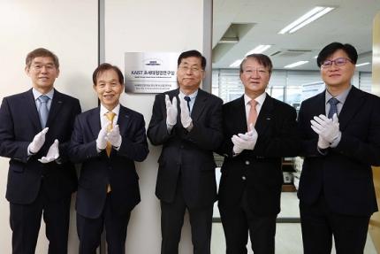
< Photo of Professor Hoi-Jun Yoo (center) of the School of Electrical Engineering at the signboard unveiling ceremony >
KAIST held a ceremony to mark the opening of three additional ‘Cross-Generation Collaborative Labs’ on the morning of January 7th, 2025.
The “Next-Generation AI Semiconductor System Lab” by Professor Hoi-Jun Yoo of the School of Electrical Engineering, the “Molecular Spectroscopy and Chemical Dynamics Lab” by Professor Sang Kyu Kim of the Department of Chemistry, and the “Advanced Data Computing Lab” by Professor Sue Bok Moon of the School of Computer Science are the three new labs given the honored titled of the “Cross-Generation Collaborative Lab”.
The Cross-Generation Collaborative Lab is KAIST’s unique system that was set up to facilitate the collaboration between retiring professors and junior professors to continue the achievements and know-how the elders have accumulated over their academic career. Since its introduction in 2018, nine labs have been named to be the Cross-Generation Labs, and this year’s new addition brings the total up to twelve.
The ‘Next-Generation AI Semiconductor System Lab’ led by Professor Hoi-Jun Yoo will be operated by Professor Joo-Young Kim of the same school.
Professor Hoi-Jun Yoo is a world-renowned scholar with outstanding research achievements in the field of on-device AI semiconductor design. Professor Joo-Young Kim is an up-and-coming researcher studying large language models and design of AI semiconductors for server computers, and is currently researching technologies to design PIM (Processing-in-Memory), a core technology in the field of AI semiconductors.
Their research goal is to systematically collaborate and transfer next-generation AI semiconductor design technology, including brain-mimicking AI algorithms such as deep neural networks and generative AI, to integrate core technologies, and to maximize the usability of R&D outputs, thereby further solidifying the position of Korean AI semiconductor companies in the global market.
Professor Hoi-Jun Yoo said, “I believe that, we will be able to present a development direction of for the next-generation AI semiconductors industries at home and abroad through collaborative research and play a key role in transferring and expanding global leadership.”
< Professor Sang Kyu Kim of the Department of Chemistry (middle), at the signboard unveiling ceremony for his laboratory >
The “Molecular Spectroscopy and Chemical Dynamics Laboratory”, where Professor Sang Kyu Kim of the Department of Chemistry is in charge, will be operated by Professor Tae Kyu Kim of the same department, and another professor in the field of spectroscopy and dynamics will join in the future.
Professor Sang Kyu Kim has secured technologies for developing unique experimental equipment based on ultrashort lasers and supersonic molecular beams, and is a world leader who has been creatively pioneering new fields of experimental physical chemistry.
The research goal is to describe chemical reactions and verify from a quantum mechanical perspective and introduce new theories and technologies to pursue a complete understanding of the principles of chemical reactions. In addition, the accompanying basic scientific knowledge will be applied to the design of new materials.
Professor Sang Kyu Kim said, “I am very happy to be able to pass on the research infrastructure to the next generation through this system, and I will continue to nurture it to grow into a world-class research lab through trans-generational collaborative research.”
< Photo of Professor Sue Bok Moon (center) at the signboard unveiling ceremony by the School of Computing >
Lastly, the “Advanced Data Computing Lab” led by Professor Sue Bok Moon is joined by Professor Mee Young Cha of the same school and Professor Wonjae Lee of the Graduate School of Culture Technology.
Professor Sue Bok Moon showed the infinite possibilities of large-scale data-based social network research through Cyworld, YouTube, and Twitter, and had a great influence on related fields beyond the field of computer science.
Professor Mee Young Cha is a data scientist who analyzes difficult social issues such as misinformation, poverty, and disaster detection using big data-based AI. She is the first Korean to be recognized for her achievements as the director of the Max Planck Institute in Germany, a world-class basic science research institute. Therefore, there is high expectation for synergy effects from overseas collaborative research and technology transfer and sharing among the participating professors of the collaborative research lab. Professor Wonjae Lee is researching dynamic interaction analysis between science and technology using structural topic models.
They plan to conduct research aimed at improving the analysis and understanding of negative influences occurring online, and in particular, developing a hateful precursor detection model using emotions and morality to preemptively block hateful expressions.
Professor Sue Bok Moon said, “Through this collaborative research lab, we will play a key role in conducting in-depth collaborative research on unexpected negative influences in the AI era so that we can have a high level of competitiveness worldwide.”
The ceremonies for the unveiling of the new Cross-Generation Collaborative Lab signboard were held in front of each lab from 10:00 AM on the 7th, in the attendance of President Kwang Hyung Lee, Senior Vice President for Research Sang Yup Lee, and other key officials of KAIST and the new staff members to join the laboratories.
2025.01.07 View 2960
“Cross-Generation Collaborative Labs” for Semiconductor, Chemistry, and Computer Science Opened
< Photo of Professor Hoi-Jun Yoo (center) of the School of Electrical Engineering at the signboard unveiling ceremony >
KAIST held a ceremony to mark the opening of three additional ‘Cross-Generation Collaborative Labs’ on the morning of January 7th, 2025.
The “Next-Generation AI Semiconductor System Lab” by Professor Hoi-Jun Yoo of the School of Electrical Engineering, the “Molecular Spectroscopy and Chemical Dynamics Lab” by Professor Sang Kyu Kim of the Department of Chemistry, and the “Advanced Data Computing Lab” by Professor Sue Bok Moon of the School of Computer Science are the three new labs given the honored titled of the “Cross-Generation Collaborative Lab”.
The Cross-Generation Collaborative Lab is KAIST’s unique system that was set up to facilitate the collaboration between retiring professors and junior professors to continue the achievements and know-how the elders have accumulated over their academic career. Since its introduction in 2018, nine labs have been named to be the Cross-Generation Labs, and this year’s new addition brings the total up to twelve.
The ‘Next-Generation AI Semiconductor System Lab’ led by Professor Hoi-Jun Yoo will be operated by Professor Joo-Young Kim of the same school.
Professor Hoi-Jun Yoo is a world-renowned scholar with outstanding research achievements in the field of on-device AI semiconductor design. Professor Joo-Young Kim is an up-and-coming researcher studying large language models and design of AI semiconductors for server computers, and is currently researching technologies to design PIM (Processing-in-Memory), a core technology in the field of AI semiconductors.
Their research goal is to systematically collaborate and transfer next-generation AI semiconductor design technology, including brain-mimicking AI algorithms such as deep neural networks and generative AI, to integrate core technologies, and to maximize the usability of R&D outputs, thereby further solidifying the position of Korean AI semiconductor companies in the global market.
Professor Hoi-Jun Yoo said, “I believe that, we will be able to present a development direction of for the next-generation AI semiconductors industries at home and abroad through collaborative research and play a key role in transferring and expanding global leadership.”
< Professor Sang Kyu Kim of the Department of Chemistry (middle), at the signboard unveiling ceremony for his laboratory >
The “Molecular Spectroscopy and Chemical Dynamics Laboratory”, where Professor Sang Kyu Kim of the Department of Chemistry is in charge, will be operated by Professor Tae Kyu Kim of the same department, and another professor in the field of spectroscopy and dynamics will join in the future.
Professor Sang Kyu Kim has secured technologies for developing unique experimental equipment based on ultrashort lasers and supersonic molecular beams, and is a world leader who has been creatively pioneering new fields of experimental physical chemistry.
The research goal is to describe chemical reactions and verify from a quantum mechanical perspective and introduce new theories and technologies to pursue a complete understanding of the principles of chemical reactions. In addition, the accompanying basic scientific knowledge will be applied to the design of new materials.
Professor Sang Kyu Kim said, “I am very happy to be able to pass on the research infrastructure to the next generation through this system, and I will continue to nurture it to grow into a world-class research lab through trans-generational collaborative research.”
< Photo of Professor Sue Bok Moon (center) at the signboard unveiling ceremony by the School of Computing >
Lastly, the “Advanced Data Computing Lab” led by Professor Sue Bok Moon is joined by Professor Mee Young Cha of the same school and Professor Wonjae Lee of the Graduate School of Culture Technology.
Professor Sue Bok Moon showed the infinite possibilities of large-scale data-based social network research through Cyworld, YouTube, and Twitter, and had a great influence on related fields beyond the field of computer science.
Professor Mee Young Cha is a data scientist who analyzes difficult social issues such as misinformation, poverty, and disaster detection using big data-based AI. She is the first Korean to be recognized for her achievements as the director of the Max Planck Institute in Germany, a world-class basic science research institute. Therefore, there is high expectation for synergy effects from overseas collaborative research and technology transfer and sharing among the participating professors of the collaborative research lab. Professor Wonjae Lee is researching dynamic interaction analysis between science and technology using structural topic models.
They plan to conduct research aimed at improving the analysis and understanding of negative influences occurring online, and in particular, developing a hateful precursor detection model using emotions and morality to preemptively block hateful expressions.
Professor Sue Bok Moon said, “Through this collaborative research lab, we will play a key role in conducting in-depth collaborative research on unexpected negative influences in the AI era so that we can have a high level of competitiveness worldwide.”
The ceremonies for the unveiling of the new Cross-Generation Collaborative Lab signboard were held in front of each lab from 10:00 AM on the 7th, in the attendance of President Kwang Hyung Lee, Senior Vice President for Research Sang Yup Lee, and other key officials of KAIST and the new staff members to join the laboratories.
2025.01.07 View 2960 -
 KAIST Scientifically Identifies a Method to Prevent Dental Erosion from Carbonated Drinks
A Korean research team, which had previously visualized and scientifically proven the harmful effects of carbonated drinks like cola on dental health using nanotechnology, has now identified a mechanism for an effective method to prevent tooth damage caused by these beverages.
KAIST (represented by President Kwang Hyung Lee) announced on the 5th of December that a team led by Professor Seungbum Hong from the Department of Materials Science and Engineering, in collaboration with Seoul National University's School of Dentistry (Departments of Pediatric Dentistry and Oral Microbiology) and Professor Hye Ryung Byon’s research team from the Department of Chemistry, has revealed through nanotechnology that silver diamine fluoride (SDF)* forms a fluoride-containing protective layer on the tooth surface, effectively inhibiting cola-induced erosion.
*SDF (Silver Diamine Fluoride): A dental agent primarily used for the treatment and prevention of tooth decay. SDF strengthens carious lesions, suppresses bacterial growth, and halts the progression of cavities.
The team analyzed the surface morphology and mechanical properties of tooth enamel on a nanoscale using atomic force microscopy (AFM). They also examined the chemical properties of the nano-film formed by SDF treatment using X-ray photoelectron spectroscopy (XPS)* and Fourier-transform infrared spectroscopy (FTIR)*.
*XPS (X-ray Photoelectron Spectroscopy): A powerful surface analysis technique used to investigate the chemical composition and electronic structure of materials.
*FTIR (Fourier-Transform Infrared Spectroscopy): An analytical method that identifies the molecular structure and composition of materials by analyzing how they absorb or transmit infrared light.
The findings showed significant differences in surface roughness and elastic modulus between teeth exposed to cola with and without SDF treatment. Teeth treated with SDF exhibited minimal changes in surface roughness due to erosion (from 64 nm to 70 nm) and maintained a high elastic modulus (from 215 GPa to 205 GPa).
This was attributed to the formation of a fluoroapatite* layer by SDF, which acted as a protective shield.
*Fluoroapatite: A phosphate mineral with the chemical formula Ca₅(PO₄)₃F (calcium fluoro-phosphate). It can occur naturally or be synthesized biologically/artificially and plays a crucial role in strengthening teeth and bones.
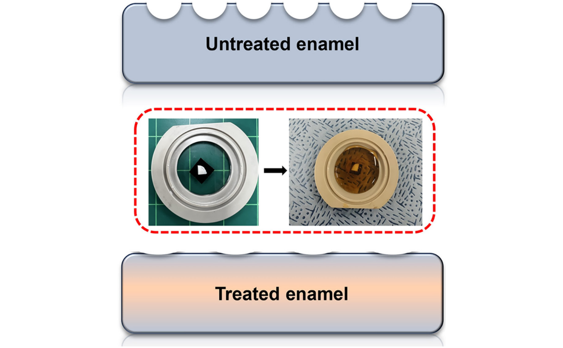
< Figure 1. Schematic of the workflow. Surface morphology and mechanical properties of untreated and treated silver diamine fluoride (SDF) treated enamel exposed to cola were analyzed over time using atomic force microscopy (AFM). >
Professor Young J. Kim from Seoul National University's Department of Pediatric Dentistry noted, "This technology could be applied to prevent dental erosion and strengthen teeth for both children and adults. It is a cost-effective and accessible dental treatment."
< Figure 2. Changes in surface roughness and elastic modulus according to time of exposure to cola for SDF untreated and treated teeth. After 1 hour, the surface roughness of the SDF untreated teeth rapidly became rougher from 83 nm to 287 nm and the elastic modulus weakened from 125 GPa to 13 GPa, whereas the surface roughness of the SDF treated teeth changed only slightly from 64 nm to 70 nm and the elastic modulus barely changed from 215 GPa to 205 GPa, maintaining a similar state to the initial state. >
Professor Seungbum Hong emphasized, "Dental health significantly impacts quality of life. This research offers an effective non-invasive method to prevent early dental erosion, moving beyond traditional surgical treatments. By simply applying SDF, dental erosion can be prevented and enamel strengthened, potentially reducing pain and costs associated with treatment."
This study, led by the first author Aditi Saha, a PhD student in KAIST’s Department of Materials Science and Engineering, was published in the international journal Biomaterials Research on November 7 under the title "Nanoscale Study on Noninvasive Prevention of Dental Erosion of Enamel by Silver Diamine Fluoride". The research was supported by the National Research Foundation of Korea.
2024.12.11 View 3232
KAIST Scientifically Identifies a Method to Prevent Dental Erosion from Carbonated Drinks
A Korean research team, which had previously visualized and scientifically proven the harmful effects of carbonated drinks like cola on dental health using nanotechnology, has now identified a mechanism for an effective method to prevent tooth damage caused by these beverages.
KAIST (represented by President Kwang Hyung Lee) announced on the 5th of December that a team led by Professor Seungbum Hong from the Department of Materials Science and Engineering, in collaboration with Seoul National University's School of Dentistry (Departments of Pediatric Dentistry and Oral Microbiology) and Professor Hye Ryung Byon’s research team from the Department of Chemistry, has revealed through nanotechnology that silver diamine fluoride (SDF)* forms a fluoride-containing protective layer on the tooth surface, effectively inhibiting cola-induced erosion.
*SDF (Silver Diamine Fluoride): A dental agent primarily used for the treatment and prevention of tooth decay. SDF strengthens carious lesions, suppresses bacterial growth, and halts the progression of cavities.
The team analyzed the surface morphology and mechanical properties of tooth enamel on a nanoscale using atomic force microscopy (AFM). They also examined the chemical properties of the nano-film formed by SDF treatment using X-ray photoelectron spectroscopy (XPS)* and Fourier-transform infrared spectroscopy (FTIR)*.
*XPS (X-ray Photoelectron Spectroscopy): A powerful surface analysis technique used to investigate the chemical composition and electronic structure of materials.
*FTIR (Fourier-Transform Infrared Spectroscopy): An analytical method that identifies the molecular structure and composition of materials by analyzing how they absorb or transmit infrared light.
The findings showed significant differences in surface roughness and elastic modulus between teeth exposed to cola with and without SDF treatment. Teeth treated with SDF exhibited minimal changes in surface roughness due to erosion (from 64 nm to 70 nm) and maintained a high elastic modulus (from 215 GPa to 205 GPa).
This was attributed to the formation of a fluoroapatite* layer by SDF, which acted as a protective shield.
*Fluoroapatite: A phosphate mineral with the chemical formula Ca₅(PO₄)₃F (calcium fluoro-phosphate). It can occur naturally or be synthesized biologically/artificially and plays a crucial role in strengthening teeth and bones.
< Figure 1. Schematic of the workflow. Surface morphology and mechanical properties of untreated and treated silver diamine fluoride (SDF) treated enamel exposed to cola were analyzed over time using atomic force microscopy (AFM). >
Professor Young J. Kim from Seoul National University's Department of Pediatric Dentistry noted, "This technology could be applied to prevent dental erosion and strengthen teeth for both children and adults. It is a cost-effective and accessible dental treatment."
< Figure 2. Changes in surface roughness and elastic modulus according to time of exposure to cola for SDF untreated and treated teeth. After 1 hour, the surface roughness of the SDF untreated teeth rapidly became rougher from 83 nm to 287 nm and the elastic modulus weakened from 125 GPa to 13 GPa, whereas the surface roughness of the SDF treated teeth changed only slightly from 64 nm to 70 nm and the elastic modulus barely changed from 215 GPa to 205 GPa, maintaining a similar state to the initial state. >
Professor Seungbum Hong emphasized, "Dental health significantly impacts quality of life. This research offers an effective non-invasive method to prevent early dental erosion, moving beyond traditional surgical treatments. By simply applying SDF, dental erosion can be prevented and enamel strengthened, potentially reducing pain and costs associated with treatment."
This study, led by the first author Aditi Saha, a PhD student in KAIST’s Department of Materials Science and Engineering, was published in the international journal Biomaterials Research on November 7 under the title "Nanoscale Study on Noninvasive Prevention of Dental Erosion of Enamel by Silver Diamine Fluoride". The research was supported by the National Research Foundation of Korea.
2024.12.11 View 3232 -
 KAIST Professor Uichin Lee Receives Distinguished Paper Award from ACM
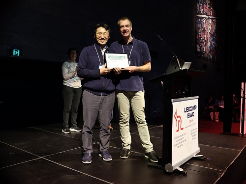
< Photo. Professor Uichin Lee (left) receiving the award >
KAIST (President Kwang Hyung Lee) announced on the 25th of October that Professor Uichin Lee’s research team from the School of Computing received the Distinguished Paper Award at the International Joint Conference on Pervasive and Ubiquitous Computing and International Symposium on Wearable Computing (Ubicomp / ISWC) hosted by the Association for Computing Machinery (ACM) in Melbourne, Australia on October 8.
The ACM Ubiquitous Computing Conference is the most prestigious international conference where leading universities and global companies from around the world present the latest research results on ubiquitous computing and wearable technologies in the field of human-computer interaction (HCI).
The main conference program is composed of invited papers published in the Proceedings of the ACM (PACM) on Interactive, Mobile, Wearable and Ubiquitous Technologies (IMWUT), which covers the latest research in the field of ubiquitous and wearable computing.
The Distinguished Paper Award Selection Committee selected eight papers among 205 papers published in Vol. 7 of the ACM Proceedings (PACM IMWUT) that made outstanding and exemplary contributions to the research community. The committee consists of 16 prominent experts who are current and former members of the journal's editorial board which made the selection after a rigorous review of all papers for a period that stretched over a month.
< Figure 1. BeActive mobile app to promote physical activity to form active lifestyle habits >
The research that won the Distinguished Paper Award was conducted by Dr. Junyoung Park, a graduate of the KAIST Graduate School of Data Science, as the 1st author, and was titled “Understanding Disengagement in Just-in-Time Mobile Health Interventions”
Professor Uichin Lee’s research team explored user engagement of ‘Just-in-Time Mobile Health Interventions’ that actively provide interventions in opportune situations by utilizing sensor data collected from health management apps, based on the premise that these apps are aptly in use to ensure effectiveness.
< Figure 2. Traditional user-requested digital behavior change intervention (DBCI) delivery (Pull) vs. Automatic transmission (Push) for Just-in-Time (JIT) mobile DBCI using smartphone sensing technologies >
The research team conducted a systematic analysis of user disengagement or the decline in user engagement in digital behavior change interventions. They developed the BeActive system, an app that promotes physical activities designed to help forming active lifestyle habits, and systematically analyzed the effects of users’ self-control ability and boredom-proneness on compliance with behavioral interventions over time.
The results of an 8-week field trial revealed that even if just-in-time interventions are provided according to the user’s situation, it is impossible to avoid a decline in participation. However, for users with high self-control and low boredom tendency, the compliance with just-in-time interventions delivered through the app was significantly higher than that of users in other groups.
In particular, users with high boredom proneness easily got tired of the repeated push interventions, and their compliance with the app decreased more quickly than in other groups.
< Figure 3. Just-in-time Mobile Health Intervention: a demonstrative case of the BeActive system: When a user is identified to be sitting for more than 50 mins, an automatic push notification is sent to recommend a short active break to complete for reward points. >
Professor Uichin Lee explained, “As the first study on user engagement in digital therapeutics and wellness services utilizing mobile just-in-time health interventions, this research provides a foundation for exploring ways to empower user engagement.” He further added, “By leveraging large language models (LLMs) and comprehensive context-aware technologies, it will be possible to develop user-centered AI technologies that can significantly boost engagement."
< Figure 4. A conceptual illustration of user engagement in digital health apps. Engagement in digital health apps consists of (1) engagement in using digital health apps and (2) engagement in behavioral interventions provided by digital health apps, i.e., compliance with behavioral interventions. Repeated adherences to behavioral interventions recommended by digital health apps can help achieve the distal health goals. >
This study was conducted with the support of the 2021 Biomedical Technology Development Program and the 2022 Basic Research and Development Program of the National Research Foundation of Korea funded by the Ministry of Science and ICT.
< Figure 5. A conceptual illustration of user disengagement and engagement of digital behavior change intervention (DBCI) apps. In general, user engagement of digital health intervention apps consists of two components: engagement in digital health apps and engagement in behavioral interventions recommended by such apps (known as behavioral compliance or intervention adherence). The distinctive stages of user can be divided into adoption, abandonment, and attrition. >
< Figure 6. Trends of changes in frequency of app usage and adherence to behavioral intervention over 8 weeks, ● SC: Self-Control Ability (High-SC: user group with high self-control, Low-SC: user group with low self-control) ● BD: Boredom-Proneness (High-BD: user group with high boredom-proneness, Low-BD: user group with low boredom-proneness). The app usage frequencies were declined over time, but the adherence rates of those participants with High-SC and Low-BD were significantly higher than other groups. >
2024.10.25 View 5328
KAIST Professor Uichin Lee Receives Distinguished Paper Award from ACM
< Photo. Professor Uichin Lee (left) receiving the award >
KAIST (President Kwang Hyung Lee) announced on the 25th of October that Professor Uichin Lee’s research team from the School of Computing received the Distinguished Paper Award at the International Joint Conference on Pervasive and Ubiquitous Computing and International Symposium on Wearable Computing (Ubicomp / ISWC) hosted by the Association for Computing Machinery (ACM) in Melbourne, Australia on October 8.
The ACM Ubiquitous Computing Conference is the most prestigious international conference where leading universities and global companies from around the world present the latest research results on ubiquitous computing and wearable technologies in the field of human-computer interaction (HCI).
The main conference program is composed of invited papers published in the Proceedings of the ACM (PACM) on Interactive, Mobile, Wearable and Ubiquitous Technologies (IMWUT), which covers the latest research in the field of ubiquitous and wearable computing.
The Distinguished Paper Award Selection Committee selected eight papers among 205 papers published in Vol. 7 of the ACM Proceedings (PACM IMWUT) that made outstanding and exemplary contributions to the research community. The committee consists of 16 prominent experts who are current and former members of the journal's editorial board which made the selection after a rigorous review of all papers for a period that stretched over a month.
< Figure 1. BeActive mobile app to promote physical activity to form active lifestyle habits >
The research that won the Distinguished Paper Award was conducted by Dr. Junyoung Park, a graduate of the KAIST Graduate School of Data Science, as the 1st author, and was titled “Understanding Disengagement in Just-in-Time Mobile Health Interventions”
Professor Uichin Lee’s research team explored user engagement of ‘Just-in-Time Mobile Health Interventions’ that actively provide interventions in opportune situations by utilizing sensor data collected from health management apps, based on the premise that these apps are aptly in use to ensure effectiveness.
< Figure 2. Traditional user-requested digital behavior change intervention (DBCI) delivery (Pull) vs. Automatic transmission (Push) for Just-in-Time (JIT) mobile DBCI using smartphone sensing technologies >
The research team conducted a systematic analysis of user disengagement or the decline in user engagement in digital behavior change interventions. They developed the BeActive system, an app that promotes physical activities designed to help forming active lifestyle habits, and systematically analyzed the effects of users’ self-control ability and boredom-proneness on compliance with behavioral interventions over time.
The results of an 8-week field trial revealed that even if just-in-time interventions are provided according to the user’s situation, it is impossible to avoid a decline in participation. However, for users with high self-control and low boredom tendency, the compliance with just-in-time interventions delivered through the app was significantly higher than that of users in other groups.
In particular, users with high boredom proneness easily got tired of the repeated push interventions, and their compliance with the app decreased more quickly than in other groups.
< Figure 3. Just-in-time Mobile Health Intervention: a demonstrative case of the BeActive system: When a user is identified to be sitting for more than 50 mins, an automatic push notification is sent to recommend a short active break to complete for reward points. >
Professor Uichin Lee explained, “As the first study on user engagement in digital therapeutics and wellness services utilizing mobile just-in-time health interventions, this research provides a foundation for exploring ways to empower user engagement.” He further added, “By leveraging large language models (LLMs) and comprehensive context-aware technologies, it will be possible to develop user-centered AI technologies that can significantly boost engagement."
< Figure 4. A conceptual illustration of user engagement in digital health apps. Engagement in digital health apps consists of (1) engagement in using digital health apps and (2) engagement in behavioral interventions provided by digital health apps, i.e., compliance with behavioral interventions. Repeated adherences to behavioral interventions recommended by digital health apps can help achieve the distal health goals. >
This study was conducted with the support of the 2021 Biomedical Technology Development Program and the 2022 Basic Research and Development Program of the National Research Foundation of Korea funded by the Ministry of Science and ICT.
< Figure 5. A conceptual illustration of user disengagement and engagement of digital behavior change intervention (DBCI) apps. In general, user engagement of digital health intervention apps consists of two components: engagement in digital health apps and engagement in behavioral interventions recommended by such apps (known as behavioral compliance or intervention adherence). The distinctive stages of user can be divided into adoption, abandonment, and attrition. >
< Figure 6. Trends of changes in frequency of app usage and adherence to behavioral intervention over 8 weeks, ● SC: Self-Control Ability (High-SC: user group with high self-control, Low-SC: user group with low self-control) ● BD: Boredom-Proneness (High-BD: user group with high boredom-proneness, Low-BD: user group with low boredom-proneness). The app usage frequencies were declined over time, but the adherence rates of those participants with High-SC and Low-BD were significantly higher than other groups. >
2024.10.25 View 5328 -
 Professor Jimin Park and Dr. Inho Kim join the ranks of the 2024 "35 Innovators Under 35" by the MIT Technology Review
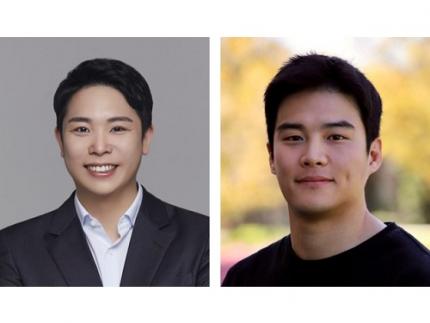
< (From left) Professor Jimin Park of the Department of Chemical and Biomolecular Engineering and Dr. Inho Kim, a graduate of the Department of Materials Science and Engineering >
KAIST (represented by President Kwang-Hyung Lee) announced on the 13th of September that Professor Jimin Park from KAIST’s Department of Chemical and Biomolecular Engineering and Dr. Inho Kim, a graduate from the Department of Materials Science and Engineering (currently a postdoctoral researcher at Caltech), were selected by the MIT Technology Review as the 2024 "35 Innovators Under 35”.
The MIT Technology Review, first published in 1899 by the Massachusetts Institute of Technology, is the world’s oldest and most influential magazine on science and technology, offering in-depth analysis across various technology fields, expanding knowledge and providing insights into cutting-edge technology trends.
Since 1999, the magazine has annually named 35 innovators under the age of 35, recognizing young talents making groundbreaking contributions in modern technology fields. The recognition is globally considered a prestigious honor and a dream for young researchers in the science and technology community.
< Image 1. Introduction for Professor Jimin Park at the Meet 35 Innovators Under 35 Summit 2024 >
Professor Jimin Park is developing next-generation bio-interfaces that link artificial materials with living organisms, and is engaged in advanced research in areas such as digital healthcare and carbon-neutral compound manufacturing technologies. In 2014, Professor Park was also recognized as one of the ‘Asia Pacific Innovators Under 35’ by the MIT Technology Review, which highlights young scientists in the Asia-Pacific region.
Professor Park responded, “It’s a great honor to be named as one of the young innovators by the MIT Technology Review, a symbol of innovation with a long history. I will continue to pursue challenging, interdisciplinary research to develop next-generation interfaces that seamlessly connect artificial materials and living organisms, from atomic to system levels.”
< Image 2. Introduction for Dr. Inho Kim as the 2024 Innovator of Materials Science for 35 Innovators Under 35 >
Dr. Inho Kim, who earned his PhD from KAIST in 2020 under the supervision of Professor Sang Ouk Kim from the Department of Materials Science and Engineering, recently succeeded in developing a new artificial muscle using composite fibers. This new material is considered the most human-like muscle ever reported in scientific literature, while also being 17 times stronger than natural human muscle.
Dr. Kim is researching the application of artificial muscle fibers in next-generation wearable assistive devices that move more naturally, like humans or animals, noting that the fibers are lightweight, flexible, and exhibit conductivity during contraction, enabling real-time feedback. Recognized for this potential, Dr. Inho Kim was named one of the '35 Innovators Under 35' this year, making him the first researcher to win the honor with the research conducted at KAIST and a PhD earned from Korea.
Dr. Kim stated, “I aim to develop robots using these new materials that can replace today’s expensive and heavy exoskeleton suits by eliminating motors and rigid frames. This will significantly reduce costs and allow for better customization, making cutting-edge technology more accessible to those who need it most, like children with cerebral palsy.”
2024.09.13 View 5485
Professor Jimin Park and Dr. Inho Kim join the ranks of the 2024 "35 Innovators Under 35" by the MIT Technology Review
< (From left) Professor Jimin Park of the Department of Chemical and Biomolecular Engineering and Dr. Inho Kim, a graduate of the Department of Materials Science and Engineering >
KAIST (represented by President Kwang-Hyung Lee) announced on the 13th of September that Professor Jimin Park from KAIST’s Department of Chemical and Biomolecular Engineering and Dr. Inho Kim, a graduate from the Department of Materials Science and Engineering (currently a postdoctoral researcher at Caltech), were selected by the MIT Technology Review as the 2024 "35 Innovators Under 35”.
The MIT Technology Review, first published in 1899 by the Massachusetts Institute of Technology, is the world’s oldest and most influential magazine on science and technology, offering in-depth analysis across various technology fields, expanding knowledge and providing insights into cutting-edge technology trends.
Since 1999, the magazine has annually named 35 innovators under the age of 35, recognizing young talents making groundbreaking contributions in modern technology fields. The recognition is globally considered a prestigious honor and a dream for young researchers in the science and technology community.
< Image 1. Introduction for Professor Jimin Park at the Meet 35 Innovators Under 35 Summit 2024 >
Professor Jimin Park is developing next-generation bio-interfaces that link artificial materials with living organisms, and is engaged in advanced research in areas such as digital healthcare and carbon-neutral compound manufacturing technologies. In 2014, Professor Park was also recognized as one of the ‘Asia Pacific Innovators Under 35’ by the MIT Technology Review, which highlights young scientists in the Asia-Pacific region.
Professor Park responded, “It’s a great honor to be named as one of the young innovators by the MIT Technology Review, a symbol of innovation with a long history. I will continue to pursue challenging, interdisciplinary research to develop next-generation interfaces that seamlessly connect artificial materials and living organisms, from atomic to system levels.”
< Image 2. Introduction for Dr. Inho Kim as the 2024 Innovator of Materials Science for 35 Innovators Under 35 >
Dr. Inho Kim, who earned his PhD from KAIST in 2020 under the supervision of Professor Sang Ouk Kim from the Department of Materials Science and Engineering, recently succeeded in developing a new artificial muscle using composite fibers. This new material is considered the most human-like muscle ever reported in scientific literature, while also being 17 times stronger than natural human muscle.
Dr. Kim is researching the application of artificial muscle fibers in next-generation wearable assistive devices that move more naturally, like humans or animals, noting that the fibers are lightweight, flexible, and exhibit conductivity during contraction, enabling real-time feedback. Recognized for this potential, Dr. Inho Kim was named one of the '35 Innovators Under 35' this year, making him the first researcher to win the honor with the research conducted at KAIST and a PhD earned from Korea.
Dr. Kim stated, “I aim to develop robots using these new materials that can replace today’s expensive and heavy exoskeleton suits by eliminating motors and rigid frames. This will significantly reduce costs and allow for better customization, making cutting-edge technology more accessible to those who need it most, like children with cerebral palsy.”
2024.09.13 View 5485 -
 KAIST finds ways for Bacteria to produce PET-like materials
Among various eco-friendly polymers, polyhydroxyalkanoates (PHA) stand out for their excellent biodegradability and biocompatibility. They decompose naturally in soil and marine environments and are used in applications such as food packaging and medical products. However, natural PHA produced to date has faced challenges meeting various physical property requirements, such as durability and thermal stability, and has been limited in its commercial application due to low production concentrations. In light of this, KAIST researchers have recently developed a technology that could play a crucial role in solving the environmental pollution problem caused by plastics.
KAIST (represented by President Kwang-Hyung Lee) announced on August 26th that a research team led by Distinguished Professor Sang Yup Lee from the Department of Chemical and Biomolecular Engineering, including Dr. Youngjoon Lee and master's student Minju Kang, has successfully developed a microbial strain that efficiently produces aromatic polyester* using systems metabolic engineering.
※ Aromatic polyester: A polymer containing aromatic compounds (specific carbon ring structures like benzene) and ester bonds.
In this study, the research team used metabolic engineering to enhance the metabolic flux of the biosynthetic pathway for the aromatic monomer phenyllactate (PhLA) in E. coli. They manipulated the metabolic pathway to increase the polymer fraction accumulated within the cells and employed computer simulations to predict the structure of PHA synthase and improve the enzyme based on the structure-function relationship.
Through subsequent fermentation optimization, the team achieved the world’s highest concentration (12.3±0.1 g/L) for the efficient production of poly (PhLA) and successfully produced polyester through a 30L scale fed-batch fermentation, demonstrating the possibility of industrial-level production. The produced aromatic polyesters showed enhanced thermal properties, improved mechanical properties, and potential for use as drug delivery carriers.
< Figure 1. Development schematics of aromatic polyester producing microorganisms >
The research team also demonstrated that an exogenous phasin protein* plays a crucial role in increasing the intracellular polymer accumulation fraction, which is directly related to the economic feasibility and efficiency of non-natural PHA production. They improved PHA synthase using a rational enzyme design approach, predicting the three-dimensional structure of the enzyme through homology modeling (a method of predicting the three-dimensional structure of a new protein based on the structure of similar proteins) followed by molecular docking simulations (simulations that predict how well a monomer can bind to an enzyme) and molecular dynamics simulations (simulations that predict how molecules move and interact over time) to upgrade the enzyme into a mutant enzyme with enhanced monomer polymerization efficiency.
※ Exogenous phasin protein: Phasin is a protein related to PHA production, interacting with the cytoplasmic environment on the surface of granules of PHA, and playing a role in polymer accumulation and controlling the number and size of granules. In this study, genes encoding phasin proteins derived from various natural PHA-producing microorganisms were selected and introduced.
Dr. Youngjoon Lee, co-first author of the paper, explained, "The significance of this study lies in the fact that we have achieved the world's highest concentration of microbial-based aromatic polyester production using eco-friendly materials and methods. This technology is expected to play a crucial role in addressing the environmental pollution caused by plastics." Distinguished Professor Sang Yup Lee added, "This study, which presents various strategies for the high-efficiency production of useful polymers via systems metabolic engineering, is expected to make a significant contribution to solving climate change issues, particularly the recent plastic problem."
< Figure 2. Detailed development strategy for aromatic polyester producing microorganisms >
The research findings were published on August 21st in Trends in Biotechnology, published by Cell, an international academic journal.
※ Paper Title: “Microbial production of an aromatic homopolyester”
※ Author Information: Youngjoon Lee (KAIST, co-first author), Minju Kang (KAIST, co-first author), Woo Dae Jang (KAIST, second author), So Young Choi (KAIST, third author), Jung Eun Yang (KAIST, fourth author), Sang Yup Lee (KAIST, corresponding author), totaling six authors.
This research was supported by the "Development of Next-Generation Biorefinery Platform Technologies for Leading the Bio-based Chemicals Industry" project led by Distinguished Professor Sang Yup Lee at KAIST, under the eco-friendly chemical technology development project aimed at substituting petroleum, funded by the Ministry of Science and ICT. It was also supported by the "Development of Platform Technology for the Production of Novel Aromatic Bioplastic Using Microbial Cell Factories" project (Project Leader: Si Jae Park, Ewha Woman’s University).
2024.08.28 View 5068
KAIST finds ways for Bacteria to produce PET-like materials
Among various eco-friendly polymers, polyhydroxyalkanoates (PHA) stand out for their excellent biodegradability and biocompatibility. They decompose naturally in soil and marine environments and are used in applications such as food packaging and medical products. However, natural PHA produced to date has faced challenges meeting various physical property requirements, such as durability and thermal stability, and has been limited in its commercial application due to low production concentrations. In light of this, KAIST researchers have recently developed a technology that could play a crucial role in solving the environmental pollution problem caused by plastics.
KAIST (represented by President Kwang-Hyung Lee) announced on August 26th that a research team led by Distinguished Professor Sang Yup Lee from the Department of Chemical and Biomolecular Engineering, including Dr. Youngjoon Lee and master's student Minju Kang, has successfully developed a microbial strain that efficiently produces aromatic polyester* using systems metabolic engineering.
※ Aromatic polyester: A polymer containing aromatic compounds (specific carbon ring structures like benzene) and ester bonds.
In this study, the research team used metabolic engineering to enhance the metabolic flux of the biosynthetic pathway for the aromatic monomer phenyllactate (PhLA) in E. coli. They manipulated the metabolic pathway to increase the polymer fraction accumulated within the cells and employed computer simulations to predict the structure of PHA synthase and improve the enzyme based on the structure-function relationship.
Through subsequent fermentation optimization, the team achieved the world’s highest concentration (12.3±0.1 g/L) for the efficient production of poly (PhLA) and successfully produced polyester through a 30L scale fed-batch fermentation, demonstrating the possibility of industrial-level production. The produced aromatic polyesters showed enhanced thermal properties, improved mechanical properties, and potential for use as drug delivery carriers.
< Figure 1. Development schematics of aromatic polyester producing microorganisms >
The research team also demonstrated that an exogenous phasin protein* plays a crucial role in increasing the intracellular polymer accumulation fraction, which is directly related to the economic feasibility and efficiency of non-natural PHA production. They improved PHA synthase using a rational enzyme design approach, predicting the three-dimensional structure of the enzyme through homology modeling (a method of predicting the three-dimensional structure of a new protein based on the structure of similar proteins) followed by molecular docking simulations (simulations that predict how well a monomer can bind to an enzyme) and molecular dynamics simulations (simulations that predict how molecules move and interact over time) to upgrade the enzyme into a mutant enzyme with enhanced monomer polymerization efficiency.
※ Exogenous phasin protein: Phasin is a protein related to PHA production, interacting with the cytoplasmic environment on the surface of granules of PHA, and playing a role in polymer accumulation and controlling the number and size of granules. In this study, genes encoding phasin proteins derived from various natural PHA-producing microorganisms were selected and introduced.
Dr. Youngjoon Lee, co-first author of the paper, explained, "The significance of this study lies in the fact that we have achieved the world's highest concentration of microbial-based aromatic polyester production using eco-friendly materials and methods. This technology is expected to play a crucial role in addressing the environmental pollution caused by plastics." Distinguished Professor Sang Yup Lee added, "This study, which presents various strategies for the high-efficiency production of useful polymers via systems metabolic engineering, is expected to make a significant contribution to solving climate change issues, particularly the recent plastic problem."
< Figure 2. Detailed development strategy for aromatic polyester producing microorganisms >
The research findings were published on August 21st in Trends in Biotechnology, published by Cell, an international academic journal.
※ Paper Title: “Microbial production of an aromatic homopolyester”
※ Author Information: Youngjoon Lee (KAIST, co-first author), Minju Kang (KAIST, co-first author), Woo Dae Jang (KAIST, second author), So Young Choi (KAIST, third author), Jung Eun Yang (KAIST, fourth author), Sang Yup Lee (KAIST, corresponding author), totaling six authors.
This research was supported by the "Development of Next-Generation Biorefinery Platform Technologies for Leading the Bio-based Chemicals Industry" project led by Distinguished Professor Sang Yup Lee at KAIST, under the eco-friendly chemical technology development project aimed at substituting petroleum, funded by the Ministry of Science and ICT. It was also supported by the "Development of Platform Technology for the Production of Novel Aromatic Bioplastic Using Microbial Cell Factories" project (Project Leader: Si Jae Park, Ewha Woman’s University).
2024.08.28 View 5068 -
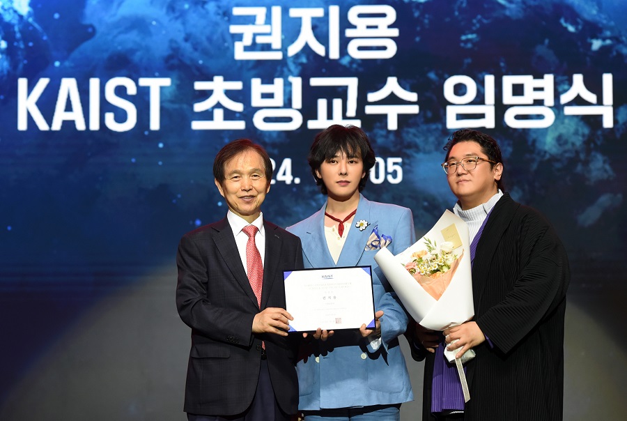 KAIST appoints K-Pop Star “G-Dragon” Kwon Ji-yong as a visiting professor
KAIST (President Kwang Hyung Lee) announced on June 5th that its Department of Mechanical Engineering has appointed Kwon Ji-yong, a K-Pop star better known as G-Dragon, as a visiting professor. The appointment was officiated at the “Innovate Korea 2024” event held at the KAIST Sports Complex in the morning of the 5th.
This appointment was promoted to expand the global competitiveness of Korean culture by applying the latest scientific technology developed from KAIST to K-content and the cultural industry.
An official from Galaxy Corporation, Mr. Kwon’s agency, said, “Through this appointment, we expect to contribute to market innovation and to the global spread and growth of K-culture through research and development of ‘entertech’*.”
* Entertech: A compound word of ‘entertainment’ and ‘technology’ refering to an industry that creates new added value by combining ICT with intellectual property rights (IP) and contents, which are the core values of entertainment.
The newly appointed Visiting Professor Kwon Ji-yong is scheduled to give a special lecture on leadership to undergraduate and graduate students. The purpose is to share his experience and life as a world-class artist to provide KAIST students with vision and insight into the world, as well as the courage and inspiration to pioneer within their own fields of expertise.
In addition, cultural events are planned to be held to help facilitate communication with KAIST members and provide artistic experiences necessary to grow into creative and convergent talents.
Joint research that applies KAIST's various technologies to art and cultural contents will also be pursued. ‘(temporarily named) KAIST-Galaxy Corporation Entertech Research Center’ will be established within the Department of Mechanical Engineering, conducting ▴research on Digital Twin technology for Korean Wave artists, starting with G-Dragon himself ▴convergent research on science and technology encompassing artificial intelligence, robots, and metaverse and K-Culture and ▴research on the development of differentiated avatars of artists using the latest technologies such as volumetrics, motion capture, and haptics.
Galaxy Corporation produces highly talked about televised shows including 'Physical: 100 Season 2', which achieved the feat of ranking first in the Netflix’s ‘Global Top 10 Non-English TV Shows’ category, as well as 'Street Woman Fighter', '2 Days & 1 Night', 'Let's Play Soccer: Mungchyeoya Chanda' and 'Mr. Trot 2', and expanded its IP (intellectual property rights) to all aspects of entertainment, from broadcasting to the music industry by recruiting G-Dragon in December last year.
It is an 'entertech' company that is pioneering a new content market by combining IP with the latest digital technologies such as metaverse, avatar, and artificial intelligence (AI). Based on these achievements, it recently signed a partnership with a global investment bank (IB). Through global investment, the company is soon to be the first entertech startup to become a unicorn (corporate value of 1 trillion won).
Kwon Ji-yong said, “It is an honor to be a visiting professor at KAIST, where countless scientific geniuses come out of. I am hoping the best of science and technology experts and my expertise in the entertainment business will come together and a great synergy, a ‘big bang’ will be ensue as a result.
“More and more musicians are working with artificial intelligence and these cutting-edge technologies enable more diverse forms of creative work,” he continued. He also expressed his specific wish. “Through the AI avatar developed jointly by Galaxy Corporation and KAIST, I wish to communicate more closely with my fans around the world that I cannot meet so often otherwise.”
President Kwang-Hyung Lee said, “Considering that KAIST is a university that has always explored new things and pioneered unknown territories since its establishment, I believe that Kwon Ji-yong also shares KAIST's DNA in that he is a leader and pioneer who has attained world-class achievements in the world of culture and arts.”
President Lee continued expressing his expectations saying, “Kwon Ji-yong will not only contribute to taking KAIST’s science and technology to spread and grow K-culture on the global stage, through his activities but also in sharing his experience and spirit as the trend leader of the world, he will be an asset to the members of KAIST which aims to become a top-tier university.”
The period of Kwon Ji-yong’s professorship is two years from the 4th of this month to June of 2026. In addition, Professor Kwon Ji-yong has been appointed as KAIST’s global ambassador to help strengthen KAIST's international presence.
Professor Kwon Ji-yong, who began his career as G-Dragon, has established himself as an icon symbolizing Korean pop culture over 18 years as a member and the leader of the K-Pop idol group 'Big Bang', which debuted in 2006 and gained global popularity. While being recognized for his outstanding ability in all aspects of his music, from writing lyrics, composing, and producing to performing, he has also been active in fashion, becoming the first Asian man to be selected as a global ambassador for Chanel in 2016, spreading Korean music and fashion to the world.
In June, 2017, he released his 3rd solo album 'Kwon Ji Yong' on USB instead of the existing CD format, for the first time in Korea. He also attended CES, the world's largest home appliance and IT exhibition held in Las Vegas, USA in January of this year, extending his strides as a 'tech-tainer'.
2024.06.05 View 16845
KAIST appoints K-Pop Star “G-Dragon” Kwon Ji-yong as a visiting professor
KAIST (President Kwang Hyung Lee) announced on June 5th that its Department of Mechanical Engineering has appointed Kwon Ji-yong, a K-Pop star better known as G-Dragon, as a visiting professor. The appointment was officiated at the “Innovate Korea 2024” event held at the KAIST Sports Complex in the morning of the 5th.
This appointment was promoted to expand the global competitiveness of Korean culture by applying the latest scientific technology developed from KAIST to K-content and the cultural industry.
An official from Galaxy Corporation, Mr. Kwon’s agency, said, “Through this appointment, we expect to contribute to market innovation and to the global spread and growth of K-culture through research and development of ‘entertech’*.”
* Entertech: A compound word of ‘entertainment’ and ‘technology’ refering to an industry that creates new added value by combining ICT with intellectual property rights (IP) and contents, which are the core values of entertainment.
The newly appointed Visiting Professor Kwon Ji-yong is scheduled to give a special lecture on leadership to undergraduate and graduate students. The purpose is to share his experience and life as a world-class artist to provide KAIST students with vision and insight into the world, as well as the courage and inspiration to pioneer within their own fields of expertise.
In addition, cultural events are planned to be held to help facilitate communication with KAIST members and provide artistic experiences necessary to grow into creative and convergent talents.
Joint research that applies KAIST's various technologies to art and cultural contents will also be pursued. ‘(temporarily named) KAIST-Galaxy Corporation Entertech Research Center’ will be established within the Department of Mechanical Engineering, conducting ▴research on Digital Twin technology for Korean Wave artists, starting with G-Dragon himself ▴convergent research on science and technology encompassing artificial intelligence, robots, and metaverse and K-Culture and ▴research on the development of differentiated avatars of artists using the latest technologies such as volumetrics, motion capture, and haptics.
Galaxy Corporation produces highly talked about televised shows including 'Physical: 100 Season 2', which achieved the feat of ranking first in the Netflix’s ‘Global Top 10 Non-English TV Shows’ category, as well as 'Street Woman Fighter', '2 Days & 1 Night', 'Let's Play Soccer: Mungchyeoya Chanda' and 'Mr. Trot 2', and expanded its IP (intellectual property rights) to all aspects of entertainment, from broadcasting to the music industry by recruiting G-Dragon in December last year.
It is an 'entertech' company that is pioneering a new content market by combining IP with the latest digital technologies such as metaverse, avatar, and artificial intelligence (AI). Based on these achievements, it recently signed a partnership with a global investment bank (IB). Through global investment, the company is soon to be the first entertech startup to become a unicorn (corporate value of 1 trillion won).
Kwon Ji-yong said, “It is an honor to be a visiting professor at KAIST, where countless scientific geniuses come out of. I am hoping the best of science and technology experts and my expertise in the entertainment business will come together and a great synergy, a ‘big bang’ will be ensue as a result.
“More and more musicians are working with artificial intelligence and these cutting-edge technologies enable more diverse forms of creative work,” he continued. He also expressed his specific wish. “Through the AI avatar developed jointly by Galaxy Corporation and KAIST, I wish to communicate more closely with my fans around the world that I cannot meet so often otherwise.”
President Kwang-Hyung Lee said, “Considering that KAIST is a university that has always explored new things and pioneered unknown territories since its establishment, I believe that Kwon Ji-yong also shares KAIST's DNA in that he is a leader and pioneer who has attained world-class achievements in the world of culture and arts.”
President Lee continued expressing his expectations saying, “Kwon Ji-yong will not only contribute to taking KAIST’s science and technology to spread and grow K-culture on the global stage, through his activities but also in sharing his experience and spirit as the trend leader of the world, he will be an asset to the members of KAIST which aims to become a top-tier university.”
The period of Kwon Ji-yong’s professorship is two years from the 4th of this month to June of 2026. In addition, Professor Kwon Ji-yong has been appointed as KAIST’s global ambassador to help strengthen KAIST's international presence.
Professor Kwon Ji-yong, who began his career as G-Dragon, has established himself as an icon symbolizing Korean pop culture over 18 years as a member and the leader of the K-Pop idol group 'Big Bang', which debuted in 2006 and gained global popularity. While being recognized for his outstanding ability in all aspects of his music, from writing lyrics, composing, and producing to performing, he has also been active in fashion, becoming the first Asian man to be selected as a global ambassador for Chanel in 2016, spreading Korean music and fashion to the world.
In June, 2017, he released his 3rd solo album 'Kwon Ji Yong' on USB instead of the existing CD format, for the first time in Korea. He also attended CES, the world's largest home appliance and IT exhibition held in Las Vegas, USA in January of this year, extending his strides as a 'tech-tainer'.
2024.06.05 View 16845 -
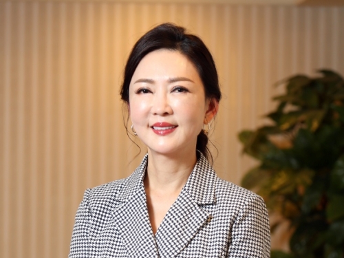 KAIST begins full-scale cooperation with Taiwan’s Formosa Group
< (From left) Senior Vice President for Planning and Budget Kyung-Soo Kim, and Professor Minee Choi of the Department of Brain and Cognitive Sciences of KAIST along with Chairman of Formosa Group Sandy Wang and KAIST President Kwang-Hyung Lee, and Dean Daesoo Kim of KAIST College of Life Science and Bioengineering >
KAIST is pursuing cooperation in the fields of advanced biotechnology and eco-friendly energy with Formosa Plastics Group, one of Taiwan's three largest companies.
To this end, Chairman Sandy Wang, a member of Formosa Group's standing committee and leader of the group's bio and eco-friendly energy sector, will visit KAIST on the 13th of this month. This is the first time that the owner of Formosa Group has made an official visit to KAIST.
Cooperation between the two institutions began last March when our university signed a memorandum of understanding on comprehensive exchange and cooperation with Ming Chi University of Science and Technology (明志科技大學), Chang Gung University(長庚大學), and Chang Gung Memorial Hospital(長庚記念醫院), three of many institutions established and supported by Formosa Group.
Based on this, Chairman Sandy Wang, who visits our university to promote more exchanges and cooperation, talked about ‘the education of children and corporate social return and practice of his father, Chairman Yung-Ching Wang,’ through a special lecture for the school leadership as a part of the Monthly Lecture on KAIST’s Leadership Innovation Day.
She then visited KAIST's research and engineering facilities related to Taiwan's future industries, such as advanced biotechnology and eco-friendly energy, and discussed global industry-academic cooperation plans. In the future, the two organizations plan to appoint adjunct professors and promote practical global cooperation, including joint student guidance and research cooperation. We plan to pursue effective mid- to long-term cooperation, such as conducting battery application research with the KAIST Next-Generation ESS Research Center and opening a graduate program specialized in stem cell and gene editing technology in connection with Chang Gung University and Chang Gung Memorial Hospital. The newly established cooperative relationship will also promote Formosa Group's investment and cooperation with KAIST's outstanding venture companies related to bio and eco-friendly energy to lay the foundation for innovative industrial cooperation between Taiwan and Korea.
President Kwang-Hyung Lee said, “The Formosa Group has a global network, so we regard it to be a key partner that will position KAIST’s bio and engineering technology in the global stages.” He also said, “With Chairman Sandy Wang’s visit, Taiwan is emerging as a global economic powerhouse,” and added, “We expect to continue our close cooperative relationship with the company.”
Formosa Group is a company founded by the late Chairman Yung-Ching Wang, the father of Chairman Sandy Wang. As the world's No. 1 plastic PVC producer, it is leading the core industries of Taiwan's economy, including semiconductors, steel, heavy industry, bio, and batteries. Chairman Yung-Ching Wang was respected by the Taiwanese people by setting an example of returning his wealth to society under the belief that the companies and assets he built ‘belonged to the people.’ Chang Gung University, Chang Gung Memorial Hospital, and Ming Chi University of Technology, which are pursuing cooperation with our university, were also established as part of the social contribution promoted by Chairman Yung-Ching Wang and are receiving financial support from Formosa Group.
2024.05.09 View 4730
KAIST begins full-scale cooperation with Taiwan’s Formosa Group
< (From left) Senior Vice President for Planning and Budget Kyung-Soo Kim, and Professor Minee Choi of the Department of Brain and Cognitive Sciences of KAIST along with Chairman of Formosa Group Sandy Wang and KAIST President Kwang-Hyung Lee, and Dean Daesoo Kim of KAIST College of Life Science and Bioengineering >
KAIST is pursuing cooperation in the fields of advanced biotechnology and eco-friendly energy with Formosa Plastics Group, one of Taiwan's three largest companies.
To this end, Chairman Sandy Wang, a member of Formosa Group's standing committee and leader of the group's bio and eco-friendly energy sector, will visit KAIST on the 13th of this month. This is the first time that the owner of Formosa Group has made an official visit to KAIST.
Cooperation between the two institutions began last March when our university signed a memorandum of understanding on comprehensive exchange and cooperation with Ming Chi University of Science and Technology (明志科技大學), Chang Gung University(長庚大學), and Chang Gung Memorial Hospital(長庚記念醫院), three of many institutions established and supported by Formosa Group.
Based on this, Chairman Sandy Wang, who visits our university to promote more exchanges and cooperation, talked about ‘the education of children and corporate social return and practice of his father, Chairman Yung-Ching Wang,’ through a special lecture for the school leadership as a part of the Monthly Lecture on KAIST’s Leadership Innovation Day.
She then visited KAIST's research and engineering facilities related to Taiwan's future industries, such as advanced biotechnology and eco-friendly energy, and discussed global industry-academic cooperation plans. In the future, the two organizations plan to appoint adjunct professors and promote practical global cooperation, including joint student guidance and research cooperation. We plan to pursue effective mid- to long-term cooperation, such as conducting battery application research with the KAIST Next-Generation ESS Research Center and opening a graduate program specialized in stem cell and gene editing technology in connection with Chang Gung University and Chang Gung Memorial Hospital. The newly established cooperative relationship will also promote Formosa Group's investment and cooperation with KAIST's outstanding venture companies related to bio and eco-friendly energy to lay the foundation for innovative industrial cooperation between Taiwan and Korea.
President Kwang-Hyung Lee said, “The Formosa Group has a global network, so we regard it to be a key partner that will position KAIST’s bio and engineering technology in the global stages.” He also said, “With Chairman Sandy Wang’s visit, Taiwan is emerging as a global economic powerhouse,” and added, “We expect to continue our close cooperative relationship with the company.”
Formosa Group is a company founded by the late Chairman Yung-Ching Wang, the father of Chairman Sandy Wang. As the world's No. 1 plastic PVC producer, it is leading the core industries of Taiwan's economy, including semiconductors, steel, heavy industry, bio, and batteries. Chairman Yung-Ching Wang was respected by the Taiwanese people by setting an example of returning his wealth to society under the belief that the companies and assets he built ‘belonged to the people.’ Chang Gung University, Chang Gung Memorial Hospital, and Ming Chi University of Technology, which are pursuing cooperation with our university, were also established as part of the social contribution promoted by Chairman Yung-Ching Wang and are receiving financial support from Formosa Group.
2024.05.09 View 4730 -
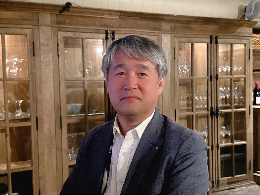 Dr. Bong-Joon Jung Elected as Interim President of KAIST U.S. Alumni Association
On April 29th, 2024, the Office of Global Initiative at KAIST, led by Vice President Man-Sung Yim, successfully conducted the election for the interim president of the KAIST U.S. Alumni Association. The authority to organize and operate the election was delegated by the KAIST U.S. Alumni Interim President Selection Committee Foundation, consisting of Je Woo Kim, Director of KAIST U.S. Foundation; Terri Kim, Director of KAIST U.S. Foundation; and Myungjin Yim, President of the KAIST Silicon Valley Alumni Association.
The election was announced during the KAIST Online U.S. Alumni Event held on December 8th, 2023, with the aim of establishing interim executive principles for six months and ultimately forming the official executive body of the KAIST U.S. Alumni Association.
The election was conducted according to the requirements set by the KAIST U.S. Alumni Interim President Selection Committee Foundation, which stated that "if there is a single candidate, they will be elected if they receive more than half of the votes from participating voters." The voting period lasted from April 13th (Monday) to April 24th (Friday) and was specifically directed towards KAIST alumni living in the Americas.
All 50 eligible voters participated in the election, unanimously supporting Dr. Bong-Joon Jung (Ph.D., admitted in 1993, Department of Electrical Engineering) with a 100% approval rate as the interim president of the KAIST U.S. Alumni Association. Dr. Bong-Joon Jung currently serves as the Senior Technology Analyst and Partner at Ambex Venture Group and previously served as the President of the KAIST Silicon Valley Alumni Association. Dr. Jung expressed his intention to strengthen connections with KAIST alumni in the United States and contribute to the establishment of the U.S. alumni association as the interim president.
< Photo. Newly elected president of interim KAIST U.S. Alumni Association, Dr. Bong-Joon Jung. >
Man-Sung Yim, Vice President of the International Office, congratulated Dr. Bong-Joon Jung on his election and pledged continuous support for the activities of the interim KAIST U.S. Alumni Association, led by alumni. He stated, "The election of the interim president of the KAIST U.S. Alumni Association marks the beginning of active engagement not only from alumni associations in various regions but also from alumni across the Americas, reflecting sustained interest in their alma mater."
2024.04.29 View 4065
Dr. Bong-Joon Jung Elected as Interim President of KAIST U.S. Alumni Association
On April 29th, 2024, the Office of Global Initiative at KAIST, led by Vice President Man-Sung Yim, successfully conducted the election for the interim president of the KAIST U.S. Alumni Association. The authority to organize and operate the election was delegated by the KAIST U.S. Alumni Interim President Selection Committee Foundation, consisting of Je Woo Kim, Director of KAIST U.S. Foundation; Terri Kim, Director of KAIST U.S. Foundation; and Myungjin Yim, President of the KAIST Silicon Valley Alumni Association.
The election was announced during the KAIST Online U.S. Alumni Event held on December 8th, 2023, with the aim of establishing interim executive principles for six months and ultimately forming the official executive body of the KAIST U.S. Alumni Association.
The election was conducted according to the requirements set by the KAIST U.S. Alumni Interim President Selection Committee Foundation, which stated that "if there is a single candidate, they will be elected if they receive more than half of the votes from participating voters." The voting period lasted from April 13th (Monday) to April 24th (Friday) and was specifically directed towards KAIST alumni living in the Americas.
All 50 eligible voters participated in the election, unanimously supporting Dr. Bong-Joon Jung (Ph.D., admitted in 1993, Department of Electrical Engineering) with a 100% approval rate as the interim president of the KAIST U.S. Alumni Association. Dr. Bong-Joon Jung currently serves as the Senior Technology Analyst and Partner at Ambex Venture Group and previously served as the President of the KAIST Silicon Valley Alumni Association. Dr. Jung expressed his intention to strengthen connections with KAIST alumni in the United States and contribute to the establishment of the U.S. alumni association as the interim president.
< Photo. Newly elected president of interim KAIST U.S. Alumni Association, Dr. Bong-Joon Jung. >
Man-Sung Yim, Vice President of the International Office, congratulated Dr. Bong-Joon Jung on his election and pledged continuous support for the activities of the interim KAIST U.S. Alumni Association, led by alumni. He stated, "The election of the interim president of the KAIST U.S. Alumni Association marks the beginning of active engagement not only from alumni associations in various regions but also from alumni across the Americas, reflecting sustained interest in their alma mater."
2024.04.29 View 4065 -
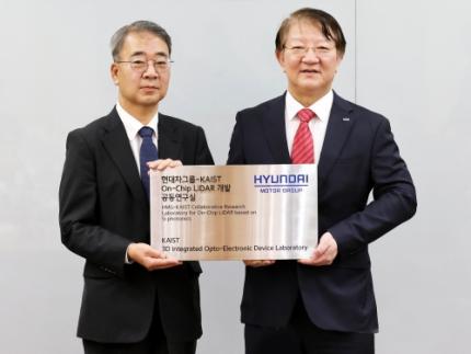 KAIST to begin Joint Research to Develop Next-Generation LiDAR System with Hyundai Motor Group
< (From left) Jong-Soo Lee, Executive Vice President at Hyundai Motor, Sang-Yup Lee, Senior Vice President for Research at KAIST >
The ‘Hyundai Motor Group-KAIST On-Chip LiDAR Joint Research Lab’ was opened at KAIST’s main campus in Daejeon to develop LiDAR sensors for advanced autonomous vehicles.
The joint research lab aims to develop high-performance and compact on-chip sensors and new signal detection technology, which are essential in the increasingly competitive autonomous driving market. On-chip sensors, which utilize semiconductor manufacturing technology to add various functions, can reduce the size of LiDAR systems compared to conventional methods and secure price competitiveness through mass production using semiconductor fabrication processes.
The joint research lab will consist of about 30 researchers, including the Hyundai-Kia Institute of Advanced Technology Development research team and KAIST professors Sanghyeon Kim, Sangsik Kim, Wanyeong Jung, and Hamza Kurt from KAIST’s School of Electrical Engineering, and will operate for four years until 2028.
KAIST will be leading the specialized work of each research team, such as for the development of silicon optoelectronic on-chip LiDAR components, the fabrication of high-speed, high-power integrated circuits to run the LiDAR systems, and the optimization and verification of LiDAR systems.
Hyundai Motor and Kia, together with Hyundai NGV, a specialized industry-academia cooperation institution, will oversee the operation of the joint research lab and provide support such as monitoring technological trends, suggesting research directions, deriving core ideas, and recommending technologies and experts to enhance research capabilities.
A Hyundai Motor Group official said, "We believe that this cooperation between Hyundai Motor Company and Kia, the leader in autonomous driving technology, and KAIST, the home of world-class technology, will hasten the achievement of fully autonomous driving." He added, "We will do our best to enable the lab to produce tangible results.”
Professor Sanghyeon Kim said, "The LiDAR sensor, which serves as the eyes of a car, is a core technology for future autonomous vehicle development that is essential for automobile companies to internalize."
2024.02.27 View 8599
KAIST to begin Joint Research to Develop Next-Generation LiDAR System with Hyundai Motor Group
< (From left) Jong-Soo Lee, Executive Vice President at Hyundai Motor, Sang-Yup Lee, Senior Vice President for Research at KAIST >
The ‘Hyundai Motor Group-KAIST On-Chip LiDAR Joint Research Lab’ was opened at KAIST’s main campus in Daejeon to develop LiDAR sensors for advanced autonomous vehicles.
The joint research lab aims to develop high-performance and compact on-chip sensors and new signal detection technology, which are essential in the increasingly competitive autonomous driving market. On-chip sensors, which utilize semiconductor manufacturing technology to add various functions, can reduce the size of LiDAR systems compared to conventional methods and secure price competitiveness through mass production using semiconductor fabrication processes.
The joint research lab will consist of about 30 researchers, including the Hyundai-Kia Institute of Advanced Technology Development research team and KAIST professors Sanghyeon Kim, Sangsik Kim, Wanyeong Jung, and Hamza Kurt from KAIST’s School of Electrical Engineering, and will operate for four years until 2028.
KAIST will be leading the specialized work of each research team, such as for the development of silicon optoelectronic on-chip LiDAR components, the fabrication of high-speed, high-power integrated circuits to run the LiDAR systems, and the optimization and verification of LiDAR systems.
Hyundai Motor and Kia, together with Hyundai NGV, a specialized industry-academia cooperation institution, will oversee the operation of the joint research lab and provide support such as monitoring technological trends, suggesting research directions, deriving core ideas, and recommending technologies and experts to enhance research capabilities.
A Hyundai Motor Group official said, "We believe that this cooperation between Hyundai Motor Company and Kia, the leader in autonomous driving technology, and KAIST, the home of world-class technology, will hasten the achievement of fully autonomous driving." He added, "We will do our best to enable the lab to produce tangible results.”
Professor Sanghyeon Kim said, "The LiDAR sensor, which serves as the eyes of a car, is a core technology for future autonomous vehicle development that is essential for automobile companies to internalize."
2024.02.27 View 8599