Electrical+Engineering
-
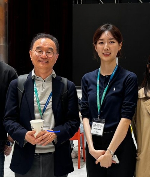 KAIST researcher Se Jin Park develops 'SpeechSSM,' opening up possibilities for a 24-hour AI voice assistant.
<(From Left)Prof. Yong Man Ro and Ph.D. candidate Sejin Park>
Se Jin Park, a researcher from Professor Yong Man Ro’s team at KAIST, has announced 'SpeechSSM', a spoken language model capable of generating long-duration speech that sounds natural and remains consistent.
An efficient processing technique based on linear sequence modeling overcomes the limitations of existing spoken language models, enabling high-quality speech generation without time constraints.
It is expected to be widely used in podcasts, audiobooks, and voice assistants due to its ability to generate natural, long-duration speech like humans.
Recently, Spoken Language Models (SLMs) have been spotlighted as next-generation technology that surpasses the limitations of text-based language models by learning human speech without text to understand and generate linguistic and non-linguistic information. However, existing models showed significant limitations in generating long-duration content required for podcasts, audiobooks, and voice assistants. Now, KAIST researcher has succeeded in overcoming these limitations by developing 'SpeechSSM,' which enables consistent and natural speech generation without time constraints.
KAIST(President Kwang Hyung Lee) announced on the 3rd of July that Ph.D. candidate Sejin Park from Professor Yong Man Ro's research team in the School of Electrical Engineering has developed 'SpeechSSM,' a spoken. a spoken language model capable of generating long-duration speech.
This research is set to be presented as an oral paper at ICML (International Conference on Machine Learning) 2025, one of the top machine learning conferences, selected among approximately 1% of all submitted papers. This not only proves outstanding research ability but also serves as an opportunity to once again demonstrate KAIST's world-leading AI research capabilities.
A major advantage of Spoken Language Models (SLMs) is their ability to directly process speech without intermediate text conversion, leveraging the unique acoustic characteristics of human speakers, allowing for the rapid generation of high-quality speech even in large-scale models.
However, existing models faced difficulties in maintaining semantic and speaker consistency for long-duration speech due to increased 'speech token resolution' and memory consumption when capturing very detailed information by breaking down speech into fine fragments.
To solve this problem, Se Jin Park developed 'SpeechSSM,' a spoken language model using a Hybrid State-Space Model, designed to efficiently process and generate long speech sequences.
This model employs a 'hybrid structure' that alternately places 'attention layers' focusing on recent information and 'recurrent layers' that remember the overall narrative flow (long-term context). This allows the story to flow smoothly without losing coherence even when generating speech for a long time. Furthermore, memory usage and computational load do not increase sharply with input length, enabling stable and efficient learning and the generation of long-duration speech.
SpeechSSM effectively processes unbounded speech sequences by dividing speech data into short, fixed units (windows), processing each unit independently, and then combining them to create long speech.
Additionally, in the speech generation phase, it uses a 'Non-Autoregressive' audio synthesis model (SoundStorm), which rapidly generates multiple parts at once instead of slowly creating one character or one word at a time, enabling the fast generation of high-quality speech.
While existing models typically evaluated short speech models of about 10 seconds, Se Jin Park created new evaluation tasks for speech generation based on their self-built benchmark dataset, 'LibriSpeech-Long,' capable of generating up to 16 minutes of speech.
Compared to PPL (Perplexity), an existing speech model evaluation metric that only indicates grammatical correctness, she proposed new evaluation metrics such as 'SC-L (semantic coherence over time)' to assess content coherence over time, and 'N-MOS-T (naturalness mean opinion score over time)' to evaluate naturalness over time, enabling more effective and precise evaluation.
Through these new evaluations, it was confirmed that speech generated by the SpeechSSM spoken language model consistently featured specific individuals mentioned in the initial prompt, and new characters and events unfolded naturally and contextually consistently, despite long-duration generation. This contrasts sharply with existing models, which tended to easily lose their topic and exhibit repetition during long-duration generation.
PhD candidate Sejin Park explained, "Existing spoken language models had limitations in long-duration generation, so our goal was to develop a spoken language model capable of generating long-duration speech for actual human use." She added, "This research achievement is expected to greatly contribute to various types of voice content creation and voice AI fields like voice assistants, by maintaining consistent content in long contexts and responding more efficiently and quickly in real time than existing methods."
This research, with Se Jin Park as the first author, was conducted in collaboration with Google DeepMind and is scheduled to be presented as an oral presentation at ICML (International Conference on Machine Learning) 2025 on July 16th.
Paper Title: Long-Form Speech Generation with Spoken Language Models
DOI: 10.48550/arXiv.2412.18603
Ph.D. candidate Se Jin Park has demonstrated outstanding research capabilities as a member of Professor Yong Man Ro's MLLM (multimodal large language model) research team, through her work integrating vision, speech, and language. Her achievements include a spotlight paper presentation at 2024 CVPR (Computer Vision and Pattern Recognition) and an Outstanding Paper Award at 2024 ACL (Association for Computational Linguistics).
For more information, you can refer to the publication and accompanying demo: SpeechSSM Publications.
2025.07.04 View 80
KAIST researcher Se Jin Park develops 'SpeechSSM,' opening up possibilities for a 24-hour AI voice assistant.
<(From Left)Prof. Yong Man Ro and Ph.D. candidate Sejin Park>
Se Jin Park, a researcher from Professor Yong Man Ro’s team at KAIST, has announced 'SpeechSSM', a spoken language model capable of generating long-duration speech that sounds natural and remains consistent.
An efficient processing technique based on linear sequence modeling overcomes the limitations of existing spoken language models, enabling high-quality speech generation without time constraints.
It is expected to be widely used in podcasts, audiobooks, and voice assistants due to its ability to generate natural, long-duration speech like humans.
Recently, Spoken Language Models (SLMs) have been spotlighted as next-generation technology that surpasses the limitations of text-based language models by learning human speech without text to understand and generate linguistic and non-linguistic information. However, existing models showed significant limitations in generating long-duration content required for podcasts, audiobooks, and voice assistants. Now, KAIST researcher has succeeded in overcoming these limitations by developing 'SpeechSSM,' which enables consistent and natural speech generation without time constraints.
KAIST(President Kwang Hyung Lee) announced on the 3rd of July that Ph.D. candidate Sejin Park from Professor Yong Man Ro's research team in the School of Electrical Engineering has developed 'SpeechSSM,' a spoken. a spoken language model capable of generating long-duration speech.
This research is set to be presented as an oral paper at ICML (International Conference on Machine Learning) 2025, one of the top machine learning conferences, selected among approximately 1% of all submitted papers. This not only proves outstanding research ability but also serves as an opportunity to once again demonstrate KAIST's world-leading AI research capabilities.
A major advantage of Spoken Language Models (SLMs) is their ability to directly process speech without intermediate text conversion, leveraging the unique acoustic characteristics of human speakers, allowing for the rapid generation of high-quality speech even in large-scale models.
However, existing models faced difficulties in maintaining semantic and speaker consistency for long-duration speech due to increased 'speech token resolution' and memory consumption when capturing very detailed information by breaking down speech into fine fragments.
To solve this problem, Se Jin Park developed 'SpeechSSM,' a spoken language model using a Hybrid State-Space Model, designed to efficiently process and generate long speech sequences.
This model employs a 'hybrid structure' that alternately places 'attention layers' focusing on recent information and 'recurrent layers' that remember the overall narrative flow (long-term context). This allows the story to flow smoothly without losing coherence even when generating speech for a long time. Furthermore, memory usage and computational load do not increase sharply with input length, enabling stable and efficient learning and the generation of long-duration speech.
SpeechSSM effectively processes unbounded speech sequences by dividing speech data into short, fixed units (windows), processing each unit independently, and then combining them to create long speech.
Additionally, in the speech generation phase, it uses a 'Non-Autoregressive' audio synthesis model (SoundStorm), which rapidly generates multiple parts at once instead of slowly creating one character or one word at a time, enabling the fast generation of high-quality speech.
While existing models typically evaluated short speech models of about 10 seconds, Se Jin Park created new evaluation tasks for speech generation based on their self-built benchmark dataset, 'LibriSpeech-Long,' capable of generating up to 16 minutes of speech.
Compared to PPL (Perplexity), an existing speech model evaluation metric that only indicates grammatical correctness, she proposed new evaluation metrics such as 'SC-L (semantic coherence over time)' to assess content coherence over time, and 'N-MOS-T (naturalness mean opinion score over time)' to evaluate naturalness over time, enabling more effective and precise evaluation.
Through these new evaluations, it was confirmed that speech generated by the SpeechSSM spoken language model consistently featured specific individuals mentioned in the initial prompt, and new characters and events unfolded naturally and contextually consistently, despite long-duration generation. This contrasts sharply with existing models, which tended to easily lose their topic and exhibit repetition during long-duration generation.
PhD candidate Sejin Park explained, "Existing spoken language models had limitations in long-duration generation, so our goal was to develop a spoken language model capable of generating long-duration speech for actual human use." She added, "This research achievement is expected to greatly contribute to various types of voice content creation and voice AI fields like voice assistants, by maintaining consistent content in long contexts and responding more efficiently and quickly in real time than existing methods."
This research, with Se Jin Park as the first author, was conducted in collaboration with Google DeepMind and is scheduled to be presented as an oral presentation at ICML (International Conference on Machine Learning) 2025 on July 16th.
Paper Title: Long-Form Speech Generation with Spoken Language Models
DOI: 10.48550/arXiv.2412.18603
Ph.D. candidate Se Jin Park has demonstrated outstanding research capabilities as a member of Professor Yong Man Ro's MLLM (multimodal large language model) research team, through her work integrating vision, speech, and language. Her achievements include a spotlight paper presentation at 2024 CVPR (Computer Vision and Pattern Recognition) and an Outstanding Paper Award at 2024 ACL (Association for Computational Linguistics).
For more information, you can refer to the publication and accompanying demo: SpeechSSM Publications.
2025.07.04 View 80 -
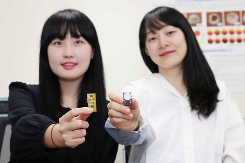 KAIST Succeeds in Real-Time Carbon Dioxide Monitoring Without Batteries or External Power
< (From left) Master's Student Gyurim Jang, Professor Kyeongha Kwon >
KAIST (President Kwang Hyung Lee) announced on June 9th that a research team led by Professor Kyeongha Kwon from the School of Electrical Engineering, in a joint study with Professor Hanjun Ryu's team at Chung-Ang University, has developed a self-powered wireless carbon dioxide (CO2) monitoring system. This innovative system harvests fine vibrational energy from its surroundings to periodically measure CO2 concentrations.
This breakthrough addresses a critical need in environmental monitoring: accurately understanding "how much" CO2 is being emitted to combat climate change and global warming. While CO2 monitoring technology is key to this, existing systems largely rely on batteries or wired power system, imposing limitations on installation and maintenance. The KAIST team tackled this by creating a self-powered wireless system that operates without external power.
The core of this new system is an "Inertia-driven Triboelectric Nanogenerator (TENG)" that converts vibrations (with amplitudes ranging from 20-4000 ㎛ and frequencies from 0-300 Hz) generated by industrial equipment or pipelines into electricity. This enables periodic CO2 concentration measurements and wireless transmission without the need for batteries.
< Figure 1. Concept and configuration of self-powered wireless CO2 monitoring system using fine vibration harvesting (a) System block diagram (b) Photo of fabricated system prototype >
The research team successfully amplified fine vibrations and induced resonance by combining spring-attached 4-stack TENGs. They achieved stable power production of 0.5 mW under conditions of 13 Hz and 0.56 g acceleration. The generated power was then used to operate a CO2 sensor and a Bluetooth Low Energy (BLE) system-on-a-chip (SoC).
Professor Kyeongha Kwon emphasized, "For efficient environmental monitoring, a system that can operate continuously without power limitations is essential." She explained, "In this research, we implemented a self-powered system that can periodically measure and wirelessly transmit CO2 concentrations based on the energy generated from an inertia-driven TENG." She added, "This technology can serve as a foundational technology for future self-powered environmental monitoring platforms integrating various sensors."
< Figure 2. TENG energy harvesting-based wireless CO2 sensing system operation results (c) Experimental setup (d) Measured CO2 concentration results powered by TENG and conventional DC power source >
This research was published on June 1st in the internationally renowned academic journal `Nano Energy (IF 16.8)`. Gyurim Jang, a master's student at KAIST, and Daniel Manaye Tiruneh, a master's student at Chung-Ang University, are the co-first authors of the paper.*Paper Title: Highly compact inertia-driven triboelectric nanogenerator for self-powered wireless CO2 monitoring via fine-vibration harvesting*DOI: 10.1016/j.nanoen.2025.110872
This research was supported by the Saudi Aramco-KAIST CO2 Management Center.
2025.06.09 View 47471
KAIST Succeeds in Real-Time Carbon Dioxide Monitoring Without Batteries or External Power
< (From left) Master's Student Gyurim Jang, Professor Kyeongha Kwon >
KAIST (President Kwang Hyung Lee) announced on June 9th that a research team led by Professor Kyeongha Kwon from the School of Electrical Engineering, in a joint study with Professor Hanjun Ryu's team at Chung-Ang University, has developed a self-powered wireless carbon dioxide (CO2) monitoring system. This innovative system harvests fine vibrational energy from its surroundings to periodically measure CO2 concentrations.
This breakthrough addresses a critical need in environmental monitoring: accurately understanding "how much" CO2 is being emitted to combat climate change and global warming. While CO2 monitoring technology is key to this, existing systems largely rely on batteries or wired power system, imposing limitations on installation and maintenance. The KAIST team tackled this by creating a self-powered wireless system that operates without external power.
The core of this new system is an "Inertia-driven Triboelectric Nanogenerator (TENG)" that converts vibrations (with amplitudes ranging from 20-4000 ㎛ and frequencies from 0-300 Hz) generated by industrial equipment or pipelines into electricity. This enables periodic CO2 concentration measurements and wireless transmission without the need for batteries.
< Figure 1. Concept and configuration of self-powered wireless CO2 monitoring system using fine vibration harvesting (a) System block diagram (b) Photo of fabricated system prototype >
The research team successfully amplified fine vibrations and induced resonance by combining spring-attached 4-stack TENGs. They achieved stable power production of 0.5 mW under conditions of 13 Hz and 0.56 g acceleration. The generated power was then used to operate a CO2 sensor and a Bluetooth Low Energy (BLE) system-on-a-chip (SoC).
Professor Kyeongha Kwon emphasized, "For efficient environmental monitoring, a system that can operate continuously without power limitations is essential." She explained, "In this research, we implemented a self-powered system that can periodically measure and wirelessly transmit CO2 concentrations based on the energy generated from an inertia-driven TENG." She added, "This technology can serve as a foundational technology for future self-powered environmental monitoring platforms integrating various sensors."
< Figure 2. TENG energy harvesting-based wireless CO2 sensing system operation results (c) Experimental setup (d) Measured CO2 concentration results powered by TENG and conventional DC power source >
This research was published on June 1st in the internationally renowned academic journal `Nano Energy (IF 16.8)`. Gyurim Jang, a master's student at KAIST, and Daniel Manaye Tiruneh, a master's student at Chung-Ang University, are the co-first authors of the paper.*Paper Title: Highly compact inertia-driven triboelectric nanogenerator for self-powered wireless CO2 monitoring via fine-vibration harvesting*DOI: 10.1016/j.nanoen.2025.110872
This research was supported by the Saudi Aramco-KAIST CO2 Management Center.
2025.06.09 View 47471 -
 KAIST Research Team Develops Electronic Ink for Room-Temperature Printing of High-Resolution, Variable-Stiffness Electronics
A team of researchers from KAIST and Seoul National University has developed a groundbreaking electronic ink that enables room-temperature printing of variable-stiffness circuits capable of switching between rigid and soft modes. This advancement marks a significant leap toward next-generation wearable, implantable, and robotic devices.
< Photo 1. (From left) Professor Jae-Woong Jeong and PhD candidate Simok Lee of the School of Electrical Engineering, (in separate bubbles, from left) Professor Gun-Hee Lee of Pusan National University, Professor Seongjun Park of Seoul National University, Professor Steve Park of the Department of Materials Science and Engineering>
Variable-stiffness electronics are at the forefront of adaptive technology, offering the ability for a single device to transition between rigid and soft modes depending on its use case. Gallium, a metal known for its high rigidity contrast between solid and liquid states, is a promising candidate for such applications. However, its use has been hindered by challenges including high surface tension, low viscosity, and undesirable phase transitions during manufacturing.
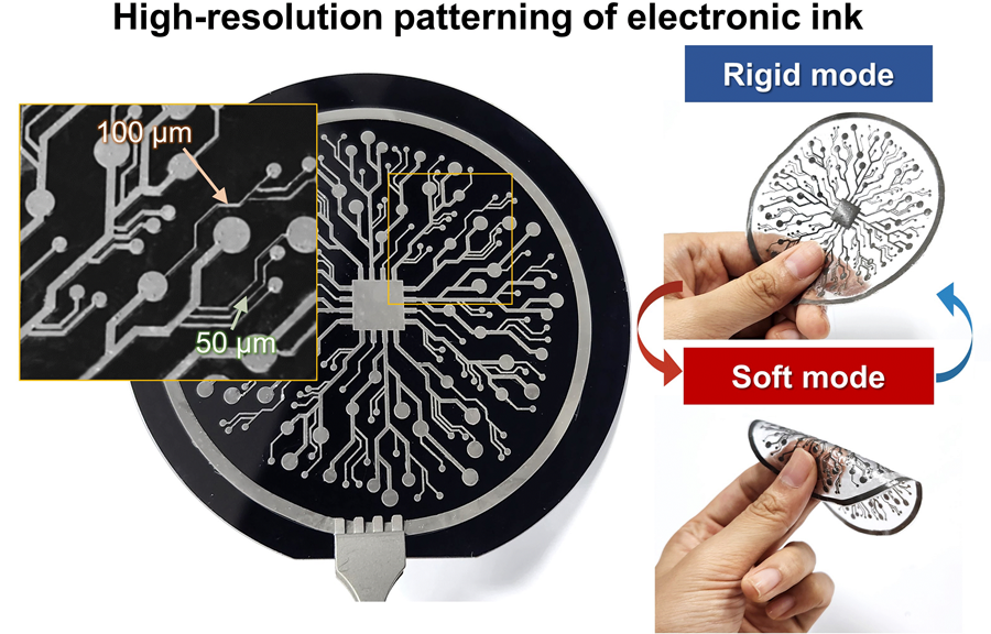
On June 4th, a research team led by Professor Jae-Woong Jeong from the School of Electrical Engineering at KAIST, Professor Seongjun Park from the Digital Healthcare Major at Seoul National University, and Professor Steve Park from the Department of Materials Science and Engineering at KAIST introduced a novel liquid metal electronic ink. This ink allows for micro-scale circuit printing – thinner than a human hair – at room temperature, with the ability to reversibly switch between rigid and soft modes depending on temperature.
The new ink combines printable viscosity with excellent electrical conductivity, enabling the creation of complex, high-resolution multilayer circuits comparable to commercial printed circuit boards (PCBs). These circuits can dynamically change stiffness in response to temperature, presenting new opportunities for multifunctional electronics, medical technologies, and robotics.
Conventional electronics typically have fixed form factors – either rigid for durability or soft for wearability. Rigid devices like smartphones and laptops offer robust performance but are uncomfortable when worn, while soft electronics are more comfortable but lack precise handling. As demand grows for devices that can adapt their stiffness to context, variable-stiffness electronics are becoming increasingly important.
< Figure 1. Fabrication process of stable, high-viscosity electronic ink by dispersing micro-sized gallium particles in a polymer matrix (left). High-resolution large-area circuit printing process through pH-controlled chemical sintering (right). >
To address this challenge, the researchers focused on gallium, which melts just below body temperature. Solid gallium is quite stiff, while its liquid form is fluid and soft. Despite its potential, gallium’s use in electronic printing has been limited by its high surface tension and instability when melted.
To overcome these issues, the team developed a pH-controlled liquid metal ink printing process. By dispersing micro-sized gallium particles into a hydrophilic polyurethane matrix using a neutral solvent (dimethyl sulfoxide, or DMSO), they created a stable, high-viscosity ink suitable for precision printing. During post-print heating, the DMSO decomposes to form an acidic environment, which removes the oxide layer on the gallium particles. This triggers the particles to coalesce into electrically conductive networks with tunable mechanical properties.
The resulting printed circuits exhibit fine feature sizes (~50 μm), high conductivity (2.27 × 10⁶ S/m), and a stiffness modulation ratio of up to 1,465 – allowing the material to shift from plastic-like rigidity to rubber-like softness. Furthermore, the ink is compatible with conventional printing techniques such as screen printing and dip coating, supporting large-area and 3D device fabrication.
< Figure 2. Key features of the electronic ink. (i) High-resolution printing and multilayer integration capability. (ii) Batch fabrication capability through large-area screen printing. (iii) Complex three-dimensional structure printing capability through dip coating. (iv) Excellent electrical conductivity and stiffness control capability.>
The team demonstrated this technology by developing a multi-functional device that operates as a rigid portable electronic under normal conditions but transforms into a soft wearable healthcare device when attached to the body. They also created a neural probe that remains stiff during surgical insertion for accurate positioning but softens once inside brain tissue to reduce inflammation – highlighting its potential for biomedical implants.
< Figure 3. Variable stiffness wearable electronics with high-resolution circuits and multilayer structure comparable to commercial printed circuit boards (PCBs). Functions as a rigid portable electronic device at room temperature, then transforms into a wearable healthcare device by softening at body temperature upon skin contact.>
“The core achievement of this research lies in overcoming the longstanding challenges of liquid metal printing through our innovative technology,” said Professor Jeong. “By controlling the ink’s acidity, we were able to electrically and mechanically connect printed gallium particles, enabling the room-temperature fabrication of high-resolution, large-area circuits with tunable stiffness. This opens up new possibilities for future personal electronics, medical devices, and robotics.”
< Figure 4. Body-temperature softening neural probe implemented by coating electronic ink on an optical waveguide structure. (Left) Remains rigid during surgery for precise manipulation and brain insertion, then softens after implantation to minimize mechanical stress on the brain and greatly enhance biocompatibility. (Right) >
This research was published in Science Advances under the title, “Phase-Change Metal Ink with pH-Controlled Chemical Sintering for Versatile and Scalable Fabrication of Variable Stiffness Electronics.” The work was supported by the National Research Foundation of Korea, the Boston-Korea Project, and the BK21 FOUR Program.
2025.06.04 View 2331
KAIST Research Team Develops Electronic Ink for Room-Temperature Printing of High-Resolution, Variable-Stiffness Electronics
A team of researchers from KAIST and Seoul National University has developed a groundbreaking electronic ink that enables room-temperature printing of variable-stiffness circuits capable of switching between rigid and soft modes. This advancement marks a significant leap toward next-generation wearable, implantable, and robotic devices.
< Photo 1. (From left) Professor Jae-Woong Jeong and PhD candidate Simok Lee of the School of Electrical Engineering, (in separate bubbles, from left) Professor Gun-Hee Lee of Pusan National University, Professor Seongjun Park of Seoul National University, Professor Steve Park of the Department of Materials Science and Engineering>
Variable-stiffness electronics are at the forefront of adaptive technology, offering the ability for a single device to transition between rigid and soft modes depending on its use case. Gallium, a metal known for its high rigidity contrast between solid and liquid states, is a promising candidate for such applications. However, its use has been hindered by challenges including high surface tension, low viscosity, and undesirable phase transitions during manufacturing.
On June 4th, a research team led by Professor Jae-Woong Jeong from the School of Electrical Engineering at KAIST, Professor Seongjun Park from the Digital Healthcare Major at Seoul National University, and Professor Steve Park from the Department of Materials Science and Engineering at KAIST introduced a novel liquid metal electronic ink. This ink allows for micro-scale circuit printing – thinner than a human hair – at room temperature, with the ability to reversibly switch between rigid and soft modes depending on temperature.
The new ink combines printable viscosity with excellent electrical conductivity, enabling the creation of complex, high-resolution multilayer circuits comparable to commercial printed circuit boards (PCBs). These circuits can dynamically change stiffness in response to temperature, presenting new opportunities for multifunctional electronics, medical technologies, and robotics.
Conventional electronics typically have fixed form factors – either rigid for durability or soft for wearability. Rigid devices like smartphones and laptops offer robust performance but are uncomfortable when worn, while soft electronics are more comfortable but lack precise handling. As demand grows for devices that can adapt their stiffness to context, variable-stiffness electronics are becoming increasingly important.
< Figure 1. Fabrication process of stable, high-viscosity electronic ink by dispersing micro-sized gallium particles in a polymer matrix (left). High-resolution large-area circuit printing process through pH-controlled chemical sintering (right). >
To address this challenge, the researchers focused on gallium, which melts just below body temperature. Solid gallium is quite stiff, while its liquid form is fluid and soft. Despite its potential, gallium’s use in electronic printing has been limited by its high surface tension and instability when melted.
To overcome these issues, the team developed a pH-controlled liquid metal ink printing process. By dispersing micro-sized gallium particles into a hydrophilic polyurethane matrix using a neutral solvent (dimethyl sulfoxide, or DMSO), they created a stable, high-viscosity ink suitable for precision printing. During post-print heating, the DMSO decomposes to form an acidic environment, which removes the oxide layer on the gallium particles. This triggers the particles to coalesce into electrically conductive networks with tunable mechanical properties.
The resulting printed circuits exhibit fine feature sizes (~50 μm), high conductivity (2.27 × 10⁶ S/m), and a stiffness modulation ratio of up to 1,465 – allowing the material to shift from plastic-like rigidity to rubber-like softness. Furthermore, the ink is compatible with conventional printing techniques such as screen printing and dip coating, supporting large-area and 3D device fabrication.
< Figure 2. Key features of the electronic ink. (i) High-resolution printing and multilayer integration capability. (ii) Batch fabrication capability through large-area screen printing. (iii) Complex three-dimensional structure printing capability through dip coating. (iv) Excellent electrical conductivity and stiffness control capability.>
The team demonstrated this technology by developing a multi-functional device that operates as a rigid portable electronic under normal conditions but transforms into a soft wearable healthcare device when attached to the body. They also created a neural probe that remains stiff during surgical insertion for accurate positioning but softens once inside brain tissue to reduce inflammation – highlighting its potential for biomedical implants.
< Figure 3. Variable stiffness wearable electronics with high-resolution circuits and multilayer structure comparable to commercial printed circuit boards (PCBs). Functions as a rigid portable electronic device at room temperature, then transforms into a wearable healthcare device by softening at body temperature upon skin contact.>
“The core achievement of this research lies in overcoming the longstanding challenges of liquid metal printing through our innovative technology,” said Professor Jeong. “By controlling the ink’s acidity, we were able to electrically and mechanically connect printed gallium particles, enabling the room-temperature fabrication of high-resolution, large-area circuits with tunable stiffness. This opens up new possibilities for future personal electronics, medical devices, and robotics.”
< Figure 4. Body-temperature softening neural probe implemented by coating electronic ink on an optical waveguide structure. (Left) Remains rigid during surgery for precise manipulation and brain insertion, then softens after implantation to minimize mechanical stress on the brain and greatly enhance biocompatibility. (Right) >
This research was published in Science Advances under the title, “Phase-Change Metal Ink with pH-Controlled Chemical Sintering for Versatile and Scalable Fabrication of Variable Stiffness Electronics.” The work was supported by the National Research Foundation of Korea, the Boston-Korea Project, and the BK21 FOUR Program.
2025.06.04 View 2331 -
 Professor Hyun Myung's Team Wins First Place in a Challenge at ICRA by IEEE
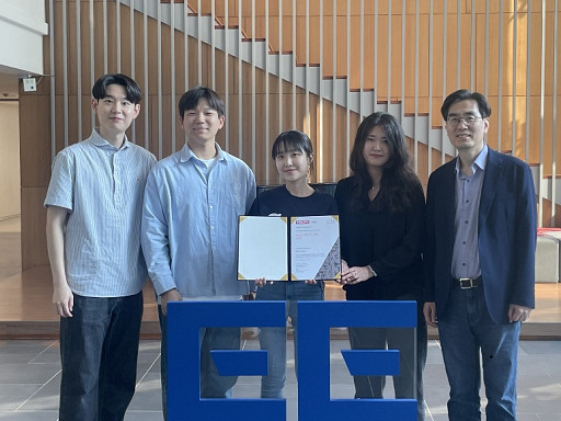
< Photo 1. (From left) Daebeom Kim (Team Leader, Ph.D. student), Seungjae Lee (Ph.D. student), Seoyeon Jang (Ph.D. student), Jei Kong (Master's student), Professor Hyun Myung >
A team of the Urban Robotics Lab, led by Professor Hyun Myung from the KAIST School of Electrical Engineering, achieved a remarkable first-place overall victory in the Nothing Stands Still Challenge (NSS Challenge) 2025, held at the 2025 IEEE International Conference on Robotics and Automation (ICRA), the world's most prestigious robotics conference, from May 19 to 23 in Atlanta, USA.
The NSS Challenge was co-hosted by HILTI, a global construction company based in Liechtenstein, and Stanford University's Gradient Spaces Group. It is an expanded version of the HILTI SLAM (Simultaneous Localization and Mapping)* Challenge, which has been held since 2021, and is considered one of the most prominent challenges at 2025 IEEE ICRA.*SLAM: Refers to Simultaneous Localization and Mapping, a technology where robots, drones, autonomous vehicles, etc., determine their own position and simultaneously create a map of their surroundings.
< Photo 2. A scene from the oral presentation on the winning team's technology (Speakers: Seungjae Lee and Seoyeon Jang, Ph.D. candidates of KAIST School of Electrical Engineering) >
This challenge primarily evaluates how accurately and robustly LiDAR scan data, collected at various times, can be registered in situations with frequent structural changes, such as construction and industrial environments. In particular, it is regarded as a highly technical competition because it deals with multi-session localization and mapping (Multi-session SLAM) technology that responds to structural changes occurring over multiple timeframes, rather than just single-point registration accuracy.
The Urban Robotics Lab team secured first place overall, surpassing National Taiwan University (3rd place) and Northwestern Polytechnical University of China (2nd place) by a significant margin, with their unique localization and mapping technology that solves the problem of registering LiDAR data collected across multiple times and spaces. The winning team will be awarded a prize of $4,000.
< Figure 1. Example of Multiway-Registration for Registering Multiple Scans >
The Urban Robotics Lab team independently developed a multiway-registration framework that can robustly register multiple scans even without prior connection information. This framework consists of an algorithm for summarizing feature points within scans and finding correspondences (CubicFeat), an algorithm for performing global registration based on the found correspondences (Quatro), and an algorithm for refining results based on change detection (Chamelion). This combination of technologies ensures stable registration performance based on fixed structures, even in highly dynamic industrial environments.
< Figure 2. Example of Change Detection Using the Chamelion Algorithm>
LiDAR scan registration technology is a core component of SLAM (Simultaneous Localization And Mapping) in various autonomous systems such as autonomous vehicles, autonomous robots, autonomous walking systems, and autonomous flying vehicles.
Professor Hyun Myung of the School of Electrical Engineering stated, "This award-winning technology is evaluated as a case that simultaneously proves both academic value and industrial applicability by maximizing the performance of precisely estimating the relative positions between different scans even in complex environments. I am grateful to the students who challenged themselves and never gave up, even when many teams abandoned due to the high difficulty."
< Figure 3. Competition Result Board, Lower RMSE (Root Mean Squared Error) Indicates Higher Score (Unit: meters)>
The Urban Robotics Lab team first participated in the SLAM Challenge in 2022, winning second place among academic teams, and in 2023, they secured first place overall in the LiDAR category and first place among academic teams in the vision category.
2025.05.30 View 2807
Professor Hyun Myung's Team Wins First Place in a Challenge at ICRA by IEEE
< Photo 1. (From left) Daebeom Kim (Team Leader, Ph.D. student), Seungjae Lee (Ph.D. student), Seoyeon Jang (Ph.D. student), Jei Kong (Master's student), Professor Hyun Myung >
A team of the Urban Robotics Lab, led by Professor Hyun Myung from the KAIST School of Electrical Engineering, achieved a remarkable first-place overall victory in the Nothing Stands Still Challenge (NSS Challenge) 2025, held at the 2025 IEEE International Conference on Robotics and Automation (ICRA), the world's most prestigious robotics conference, from May 19 to 23 in Atlanta, USA.
The NSS Challenge was co-hosted by HILTI, a global construction company based in Liechtenstein, and Stanford University's Gradient Spaces Group. It is an expanded version of the HILTI SLAM (Simultaneous Localization and Mapping)* Challenge, which has been held since 2021, and is considered one of the most prominent challenges at 2025 IEEE ICRA.*SLAM: Refers to Simultaneous Localization and Mapping, a technology where robots, drones, autonomous vehicles, etc., determine their own position and simultaneously create a map of their surroundings.
< Photo 2. A scene from the oral presentation on the winning team's technology (Speakers: Seungjae Lee and Seoyeon Jang, Ph.D. candidates of KAIST School of Electrical Engineering) >
This challenge primarily evaluates how accurately and robustly LiDAR scan data, collected at various times, can be registered in situations with frequent structural changes, such as construction and industrial environments. In particular, it is regarded as a highly technical competition because it deals with multi-session localization and mapping (Multi-session SLAM) technology that responds to structural changes occurring over multiple timeframes, rather than just single-point registration accuracy.
The Urban Robotics Lab team secured first place overall, surpassing National Taiwan University (3rd place) and Northwestern Polytechnical University of China (2nd place) by a significant margin, with their unique localization and mapping technology that solves the problem of registering LiDAR data collected across multiple times and spaces. The winning team will be awarded a prize of $4,000.
< Figure 1. Example of Multiway-Registration for Registering Multiple Scans >
The Urban Robotics Lab team independently developed a multiway-registration framework that can robustly register multiple scans even without prior connection information. This framework consists of an algorithm for summarizing feature points within scans and finding correspondences (CubicFeat), an algorithm for performing global registration based on the found correspondences (Quatro), and an algorithm for refining results based on change detection (Chamelion). This combination of technologies ensures stable registration performance based on fixed structures, even in highly dynamic industrial environments.
< Figure 2. Example of Change Detection Using the Chamelion Algorithm>
LiDAR scan registration technology is a core component of SLAM (Simultaneous Localization And Mapping) in various autonomous systems such as autonomous vehicles, autonomous robots, autonomous walking systems, and autonomous flying vehicles.
Professor Hyun Myung of the School of Electrical Engineering stated, "This award-winning technology is evaluated as a case that simultaneously proves both academic value and industrial applicability by maximizing the performance of precisely estimating the relative positions between different scans even in complex environments. I am grateful to the students who challenged themselves and never gave up, even when many teams abandoned due to the high difficulty."
< Figure 3. Competition Result Board, Lower RMSE (Root Mean Squared Error) Indicates Higher Score (Unit: meters)>
The Urban Robotics Lab team first participated in the SLAM Challenge in 2022, winning second place among academic teams, and in 2023, they secured first place overall in the LiDAR category and first place among academic teams in the vision category.
2025.05.30 View 2807 -
 KAIST & CMU Unveils Amuse, a Songwriting AI-Collaborator to Help Create Music
Wouldn't it be great if music creators had someone to brainstorm with, help them when they're stuck, and explore different musical directions together? Researchers of KAIST and Carnegie Mellon University (CMU) have developed AI technology similar to a fellow songwriter who helps create music.
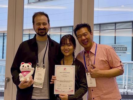
KAIST (President Kwang-Hyung Lee) has developed an AI-based music creation support system, Amuse, by a research team led by Professor Sung-Ju Lee of the School of Electrical Engineering in collaboration with CMU. The research was presented at the ACM Conference on Human Factors in Computing Systems (CHI), one of the world’s top conferences in human-computer interaction, held in Yokohama, Japan from April 26 to May 1. It received the Best Paper Award, given to only the top 1% of all submissions.
< (From left) Professor Chris Donahue of Carnegie Mellon University, Ph.D. Student Yewon Kim and Professor Sung-Ju Lee of the School of Electrical Engineering >
The system developed by Professor Sung-Ju Lee’s research team, Amuse, is an AI-based system that converts various forms of inspiration such as text, images, and audio into harmonic structures (chord progressions) to support composition.
For example, if a user inputs a phrase, image, or sound clip such as “memories of a warm summer beach”, Amuse automatically generates and suggests chord progressions that match the inspiration.
Unlike existing generative AI, Amuse is differentiated in that it respects the user's creative flow and naturally induces creative exploration through an interactive method that allows flexible integration and modification of AI suggestions.
The core technology of the Amuse system is a generation method that blends two approaches: a large language model creates music code based on the user's prompt and inspiration, while another AI model, trained on real music data, filters out awkward or unnatural results using rejection sampling.
< Figure 1. Amuse system configuration. After extracting music keywords from user input, a large language model-based code progression is generated and refined through rejection sampling (left). Code extraction from audio input is also possible (right). The bottom is an example visualizing the chord structure of the generated code. >
The research team conducted a user study targeting actual musicians and evaluated that Amuse has high potential as a creative companion, or a Co-Creative AI, a concept in which people and AI collaborate, rather than having a generative AI simply put together a song.
The paper, in which a Ph.D. student Yewon Kim and Professor Sung-Ju Lee of KAIST School of Electrical and Electronic Engineering and Carnegie Mellon University Professor Chris Donahue participated, demonstrated the potential of creative AI system design in both academia and industry. ※ Paper title: Amuse: Human-AI Collaborative Songwriting with Multimodal Inspirations DOI: https://doi.org/10.1145/3706598.3713818
※ Research demo video: https://youtu.be/udilkRSnftI?si=FNXccC9EjxHOCrm1
※ Research homepage: https://nmsl.kaist.ac.kr/projects/amuse/
Professor Sung-Ju Lee said, “Recent generative AI technology has raised concerns in that it directly imitates copyrighted content, thereby violating the copyright of the creator, or generating results one-way regardless of the creator’s intention. Accordingly, the research team was aware of this trend, paid attention to what the creator actually needs, and focused on designing an AI system centered on the creator.”
He continued, “Amuse is an attempt to explore the possibility of collaboration with AI while maintaining the initiative of the creator, and is expected to be a starting point for suggesting a more creator-friendly direction in the development of music creation tools and generative AI systems in the future.”
This research was conducted with the support of the National Research Foundation of Korea with funding from the government (Ministry of Science and ICT). (RS-2024-00337007)
2025.05.07 View 5137
KAIST & CMU Unveils Amuse, a Songwriting AI-Collaborator to Help Create Music
Wouldn't it be great if music creators had someone to brainstorm with, help them when they're stuck, and explore different musical directions together? Researchers of KAIST and Carnegie Mellon University (CMU) have developed AI technology similar to a fellow songwriter who helps create music.
KAIST (President Kwang-Hyung Lee) has developed an AI-based music creation support system, Amuse, by a research team led by Professor Sung-Ju Lee of the School of Electrical Engineering in collaboration with CMU. The research was presented at the ACM Conference on Human Factors in Computing Systems (CHI), one of the world’s top conferences in human-computer interaction, held in Yokohama, Japan from April 26 to May 1. It received the Best Paper Award, given to only the top 1% of all submissions.
< (From left) Professor Chris Donahue of Carnegie Mellon University, Ph.D. Student Yewon Kim and Professor Sung-Ju Lee of the School of Electrical Engineering >
The system developed by Professor Sung-Ju Lee’s research team, Amuse, is an AI-based system that converts various forms of inspiration such as text, images, and audio into harmonic structures (chord progressions) to support composition.
For example, if a user inputs a phrase, image, or sound clip such as “memories of a warm summer beach”, Amuse automatically generates and suggests chord progressions that match the inspiration.
Unlike existing generative AI, Amuse is differentiated in that it respects the user's creative flow and naturally induces creative exploration through an interactive method that allows flexible integration and modification of AI suggestions.
The core technology of the Amuse system is a generation method that blends two approaches: a large language model creates music code based on the user's prompt and inspiration, while another AI model, trained on real music data, filters out awkward or unnatural results using rejection sampling.
< Figure 1. Amuse system configuration. After extracting music keywords from user input, a large language model-based code progression is generated and refined through rejection sampling (left). Code extraction from audio input is also possible (right). The bottom is an example visualizing the chord structure of the generated code. >
The research team conducted a user study targeting actual musicians and evaluated that Amuse has high potential as a creative companion, or a Co-Creative AI, a concept in which people and AI collaborate, rather than having a generative AI simply put together a song.
The paper, in which a Ph.D. student Yewon Kim and Professor Sung-Ju Lee of KAIST School of Electrical and Electronic Engineering and Carnegie Mellon University Professor Chris Donahue participated, demonstrated the potential of creative AI system design in both academia and industry. ※ Paper title: Amuse: Human-AI Collaborative Songwriting with Multimodal Inspirations DOI: https://doi.org/10.1145/3706598.3713818
※ Research demo video: https://youtu.be/udilkRSnftI?si=FNXccC9EjxHOCrm1
※ Research homepage: https://nmsl.kaist.ac.kr/projects/amuse/
Professor Sung-Ju Lee said, “Recent generative AI technology has raised concerns in that it directly imitates copyrighted content, thereby violating the copyright of the creator, or generating results one-way regardless of the creator’s intention. Accordingly, the research team was aware of this trend, paid attention to what the creator actually needs, and focused on designing an AI system centered on the creator.”
He continued, “Amuse is an attempt to explore the possibility of collaboration with AI while maintaining the initiative of the creator, and is expected to be a starting point for suggesting a more creator-friendly direction in the development of music creation tools and generative AI systems in the future.”
This research was conducted with the support of the National Research Foundation of Korea with funding from the government (Ministry of Science and ICT). (RS-2024-00337007)
2025.05.07 View 5137 -
 KAIST Innovates Mid-Infrared Photodetectors for Exoplanet Detection, Expanding Applications to Environmental and Medical Fields
NASA’s James Webb Space Telescope (JWST) utilizes mid-infrared spectroscopy to precisely analyze molecular components such as water vapor and sulfur dioxide in exoplanet atmospheres. The key to this analysis, where each molecule exhibits a unique spectral "fingerprint," lies in highly sensitive photodetector technology capable of measuring extremely weak light intensities. Recently, KAIST researchers have developed an innovative photodetector capable of detecting a broad range of mid-infrared spectra, garnering significant attention.
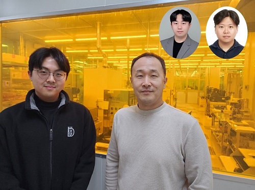
< Photo 1. (from the left) Ph.D. candidate Inki Kim (co-author), Professor SangHyeon Kim (corresponding author), Dr. Joonsup Shim (first author), and Dr. Jinha Lim (co-author) of KAIST School of Electrical Engineering. >
KAIST (represented by President Kwang-Hyung Lee) announced on the 27th of March that a research team led by Professor SangHyeon Kim from the School of Electrical Engineering has developed a mid-infrared photodetector that operates stably at room temperature, marking a major turning point for the commercialization of ultra-compact optical sensors.
The newly developed photodetector utilizes conventional silicon-based CMOS processes, enabling low-cost mass production while maintaining stable operation at room temperature. Notably, the research team successfully demonstrated the real-time detection of carbon dioxide (CO₂) gas using ultra-compact and ultra-thin optical sensors equipped with this photodetector, proving its potential for environmental monitoring and hazardous gas analysis.
Existing mid-infrared photodetectors generally require cooling systems due to high thermal noise at room temperature. These cooling systems increase the size and cost of equipment, making miniaturization and integration into portable devices challenging. Furthermore, conventional mid-infrared photodetectors are incompatible with silicon-based CMOS processes, limiting large-scale production and commercialization.
To address these limitations, the research team developed a waveguide-integrated photodetector using germanium (Ge), a Group IV element like silicon. This approach enables broad-spectrum mid-infrared detection while ensuring stable operation at room temperature.
< Figure 1. Schematic diagram of a room-temperature mid-infrared waveguide-integrated photodetector based on the Ge-on-insulator optical platform proposed in this study (top). Optical microscope image of the integrated photodetector connected with the sensing unit (bottom). >
A waveguide is a structure designed to efficiently guide light along a specific path with minimal loss. To implement various optical functions on a chip (on-chip), the development of waveguide-integrated photodetectors and waveguide-based optical components is essential.
Unlike conventional photodetectors that primarily rely on bandgap absorption principles, this new technology leverages the bolometric effect*, allowing it to detect the entire mid-infrared spectral range. As a result, it can be widely applied to the real-time sensing of various molecular species.
*Bolometric effect: A principle in which light absorption leads to an increase in temperature, causing electrical signals to change accordingly.
The waveguide-integrated mid-infrared photodetector developed by the research team is considered a groundbreaking innovation that overcomes the limitations of existing mid-infrared sensor technologies, including the need for cooling, difficulties in mass production, and high costs.
< Figure 2. Room temperature photoresponse characteristics of the mid-infrared waveguide photodetector proposed in this study (left) and real-time carbon dioxide (CO2) gas sensing results using the photodetector (right). >
This breakthrough technology is expected to be applicable across diverse fields, including environmental monitoring, medical diagnostics, industrial process management, national defense and security, and smart devices. It also paves the way for next-generation mid-infrared sensor advancements.
Professor SangHyeon Kim from KAIST stated, "This research represents a novel approach that overcomes the limitations of existing mid-infrared photodetector technologies and has great potential for practical applications in various fields." He further emphasized, "Since this sensor technology is compatible with CMOS processes, it enables low-cost mass production, making it highly suitable for next-generation environmental monitoring systems and smart manufacturing sites."
< Figure 3. Performance comparison image of a room-temperature mid-infrared waveguide photodetector fabricated with the technology proposed in this study. It achieves the world’s highest performance compared to existing technologies utilizing the Bolometric effect, and is the only solution compatible with CMOS processes. The technology proposed by our research team is characterized by its ability to respond to a wide spectrum of the mid-infrared band without limitations. >
The study, with Dr. Joonsup Shim (currently a postdoctoral researcher at Harvard University) as the first author, was published on March 19, 2025 in the internationally renowned journal Light: Science & Applications (JCR 2.9%, IF=20.6).
(Paper title: “Room-temperature waveguide-integrated photodetector using bolometric effect for mid-infrared spectroscopy applications,” https://doi.org/10.1038/s41377-025-01803-3)
2025.03.27 View 2975
KAIST Innovates Mid-Infrared Photodetectors for Exoplanet Detection, Expanding Applications to Environmental and Medical Fields
NASA’s James Webb Space Telescope (JWST) utilizes mid-infrared spectroscopy to precisely analyze molecular components such as water vapor and sulfur dioxide in exoplanet atmospheres. The key to this analysis, where each molecule exhibits a unique spectral "fingerprint," lies in highly sensitive photodetector technology capable of measuring extremely weak light intensities. Recently, KAIST researchers have developed an innovative photodetector capable of detecting a broad range of mid-infrared spectra, garnering significant attention.
< Photo 1. (from the left) Ph.D. candidate Inki Kim (co-author), Professor SangHyeon Kim (corresponding author), Dr. Joonsup Shim (first author), and Dr. Jinha Lim (co-author) of KAIST School of Electrical Engineering. >
KAIST (represented by President Kwang-Hyung Lee) announced on the 27th of March that a research team led by Professor SangHyeon Kim from the School of Electrical Engineering has developed a mid-infrared photodetector that operates stably at room temperature, marking a major turning point for the commercialization of ultra-compact optical sensors.
The newly developed photodetector utilizes conventional silicon-based CMOS processes, enabling low-cost mass production while maintaining stable operation at room temperature. Notably, the research team successfully demonstrated the real-time detection of carbon dioxide (CO₂) gas using ultra-compact and ultra-thin optical sensors equipped with this photodetector, proving its potential for environmental monitoring and hazardous gas analysis.
Existing mid-infrared photodetectors generally require cooling systems due to high thermal noise at room temperature. These cooling systems increase the size and cost of equipment, making miniaturization and integration into portable devices challenging. Furthermore, conventional mid-infrared photodetectors are incompatible with silicon-based CMOS processes, limiting large-scale production and commercialization.
To address these limitations, the research team developed a waveguide-integrated photodetector using germanium (Ge), a Group IV element like silicon. This approach enables broad-spectrum mid-infrared detection while ensuring stable operation at room temperature.
< Figure 1. Schematic diagram of a room-temperature mid-infrared waveguide-integrated photodetector based on the Ge-on-insulator optical platform proposed in this study (top). Optical microscope image of the integrated photodetector connected with the sensing unit (bottom). >
A waveguide is a structure designed to efficiently guide light along a specific path with minimal loss. To implement various optical functions on a chip (on-chip), the development of waveguide-integrated photodetectors and waveguide-based optical components is essential.
Unlike conventional photodetectors that primarily rely on bandgap absorption principles, this new technology leverages the bolometric effect*, allowing it to detect the entire mid-infrared spectral range. As a result, it can be widely applied to the real-time sensing of various molecular species.
*Bolometric effect: A principle in which light absorption leads to an increase in temperature, causing electrical signals to change accordingly.
The waveguide-integrated mid-infrared photodetector developed by the research team is considered a groundbreaking innovation that overcomes the limitations of existing mid-infrared sensor technologies, including the need for cooling, difficulties in mass production, and high costs.
< Figure 2. Room temperature photoresponse characteristics of the mid-infrared waveguide photodetector proposed in this study (left) and real-time carbon dioxide (CO2) gas sensing results using the photodetector (right). >
This breakthrough technology is expected to be applicable across diverse fields, including environmental monitoring, medical diagnostics, industrial process management, national defense and security, and smart devices. It also paves the way for next-generation mid-infrared sensor advancements.
Professor SangHyeon Kim from KAIST stated, "This research represents a novel approach that overcomes the limitations of existing mid-infrared photodetector technologies and has great potential for practical applications in various fields." He further emphasized, "Since this sensor technology is compatible with CMOS processes, it enables low-cost mass production, making it highly suitable for next-generation environmental monitoring systems and smart manufacturing sites."
< Figure 3. Performance comparison image of a room-temperature mid-infrared waveguide photodetector fabricated with the technology proposed in this study. It achieves the world’s highest performance compared to existing technologies utilizing the Bolometric effect, and is the only solution compatible with CMOS processes. The technology proposed by our research team is characterized by its ability to respond to a wide spectrum of the mid-infrared band without limitations. >
The study, with Dr. Joonsup Shim (currently a postdoctoral researcher at Harvard University) as the first author, was published on March 19, 2025 in the internationally renowned journal Light: Science & Applications (JCR 2.9%, IF=20.6).
(Paper title: “Room-temperature waveguide-integrated photodetector using bolometric effect for mid-infrared spectroscopy applications,” https://doi.org/10.1038/s41377-025-01803-3)
2025.03.27 View 2975 -
 No More Touch Issues on Rainy Days! KAIST Develops Human-Like Tactile Sensor
Recent advancements in robotics have enabled machines to handle delicate objects like eggs with precision, thanks to highly integrated pressure sensors that provide detailed tactile feedback. However, even the most advanced robots struggle to accurately detect pressure in complex environments involving water, bending, or electromagnetic interference. A research team at KAIST has successfully developed a pressure sensor that operates stably without external interference, even on wet surfaces like a smartphone screen covered in water, achieving human-level tactile sensitivity.
KAIST (represented by President Kwang Hyung Lee) announced on the 10th of March that a research team led by Professor Jun-Bo Yoon from the School of Electrical Engineering has developed a high-resolution pressure sensor that remains unaffected by external interference such as "ghost touches" caused by moisture on touchscreens.
Capacitive pressure sensors, widely used in touch systems due to their simple structure and durability, are essential components of human-machine interface (HMI) technologies in smartphones, wearable devices, and robots. However, they are prone to malfunctions caused by water droplets, electromagnetic interference, and curves.
To address these issues, the research team investigated the root causes of interference in capacitive pressure sensors. They identified that the "fringe field" generated at the sensor’s edges is particularly susceptible to external disturbances.
The researchers concluded that, to fundamentally resolve this issue, suppressing the fringe field was necessary. Through theoretical analysis, they determined that reducing the electrode spacing to the nanometer scale could effectively minimize the fringe field to below a few percent.
Utilizing proprietary micro/nanofabrication techniques, the team developed a nanogap pressure sensor with an electrode spacing of 900 nanometers (nm). This newly developed sensor reliably detected pressure regardless of the material exerting force and remained unaffected by bending or electromagnetic interference.
Furthermore, the team successfully implemented an artificial tactile system utilizing the developed sensor’s characteristics. Human skin contains specialized pressure receptors called Merkel’s disks. To artificially mimic them, the exclusive detection of pressure was necessary, but hadn’t been achieved by conventional sensors.
Professor Yoon’s research team overcame these challenges, developing a sensor achieving a density comparable to Merkel’s discs and enabling wireless, high-precision pressure sensing.
To explore potential applications, the researcher also developed a force touch pad system, demonstrating its ability to capture pressure magnitude and distribution with high resolution and without interference.
Professor Yoon stated, “Our nanogap pressure sensor operates reliably even in rainy conditions or sweaty environments, eliminating common touch malfunctions. We believe this innovation will significantly enhance everyday user experiences.”
He added, “This technology has the potential to revolutionize various fields, including precision tactile sensors for robotics, medical wearable devices, and next-generation augmented reality (AR) and virtual reality (VR) interfaces.”
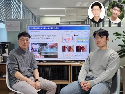
The study was led by Jae-Soon Yang (Ph.D.), Myung-Kun Chung (Ph.D. candidate), and Jae-Young Yoo (Assistant Professor at Sungkyunkwan University, a KAIST Ph.D. graduate). The research findings were published in Nature Communications on February 27, 2025. (Paper title: “Interference-Free Nanogap Pressure Sensor Array with High Spatial Resolution for Wireless Human-Machine Interface Applications”, DOI: 10.1038/s41467-025-57232-8)
This study was supported by the National Research Foundation of Korea’s Mid-Career Researcher Program and Leading Research Center Support Program.
2025.03.14 View 3693
No More Touch Issues on Rainy Days! KAIST Develops Human-Like Tactile Sensor
Recent advancements in robotics have enabled machines to handle delicate objects like eggs with precision, thanks to highly integrated pressure sensors that provide detailed tactile feedback. However, even the most advanced robots struggle to accurately detect pressure in complex environments involving water, bending, or electromagnetic interference. A research team at KAIST has successfully developed a pressure sensor that operates stably without external interference, even on wet surfaces like a smartphone screen covered in water, achieving human-level tactile sensitivity.
KAIST (represented by President Kwang Hyung Lee) announced on the 10th of March that a research team led by Professor Jun-Bo Yoon from the School of Electrical Engineering has developed a high-resolution pressure sensor that remains unaffected by external interference such as "ghost touches" caused by moisture on touchscreens.
Capacitive pressure sensors, widely used in touch systems due to their simple structure and durability, are essential components of human-machine interface (HMI) technologies in smartphones, wearable devices, and robots. However, they are prone to malfunctions caused by water droplets, electromagnetic interference, and curves.
To address these issues, the research team investigated the root causes of interference in capacitive pressure sensors. They identified that the "fringe field" generated at the sensor’s edges is particularly susceptible to external disturbances.
The researchers concluded that, to fundamentally resolve this issue, suppressing the fringe field was necessary. Through theoretical analysis, they determined that reducing the electrode spacing to the nanometer scale could effectively minimize the fringe field to below a few percent.
Utilizing proprietary micro/nanofabrication techniques, the team developed a nanogap pressure sensor with an electrode spacing of 900 nanometers (nm). This newly developed sensor reliably detected pressure regardless of the material exerting force and remained unaffected by bending or electromagnetic interference.
Furthermore, the team successfully implemented an artificial tactile system utilizing the developed sensor’s characteristics. Human skin contains specialized pressure receptors called Merkel’s disks. To artificially mimic them, the exclusive detection of pressure was necessary, but hadn’t been achieved by conventional sensors.
Professor Yoon’s research team overcame these challenges, developing a sensor achieving a density comparable to Merkel’s discs and enabling wireless, high-precision pressure sensing.
To explore potential applications, the researcher also developed a force touch pad system, demonstrating its ability to capture pressure magnitude and distribution with high resolution and without interference.
Professor Yoon stated, “Our nanogap pressure sensor operates reliably even in rainy conditions or sweaty environments, eliminating common touch malfunctions. We believe this innovation will significantly enhance everyday user experiences.”
He added, “This technology has the potential to revolutionize various fields, including precision tactile sensors for robotics, medical wearable devices, and next-generation augmented reality (AR) and virtual reality (VR) interfaces.”
The study was led by Jae-Soon Yang (Ph.D.), Myung-Kun Chung (Ph.D. candidate), and Jae-Young Yoo (Assistant Professor at Sungkyunkwan University, a KAIST Ph.D. graduate). The research findings were published in Nature Communications on February 27, 2025. (Paper title: “Interference-Free Nanogap Pressure Sensor Array with High Spatial Resolution for Wireless Human-Machine Interface Applications”, DOI: 10.1038/s41467-025-57232-8)
This study was supported by the National Research Foundation of Korea’s Mid-Career Researcher Program and Leading Research Center Support Program.
2025.03.14 View 3693 -
 KAIST Develops Wearable Carbon Dioxide Sensor to Enable Real-time Apnea Diagnosis
- Professor Seunghyup Yoo’s research team of the School of Electrical Engineering developed an ultralow-power carbon dioxide (CO2) sensor using a flexible and thin organic photodiode, and succeeded in real-time breathing monitoring by attaching it to a commercial mask
- Wearable devices with features such as low power, high stability, and flexibility can be utilized for early diagnosis of various diseases such as chronic obstructive pulmonary disease and sleep apnea
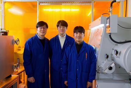
< Photo 1. From the left, School of Electrical Engineering, Ph.D. candidate DongHo Choi, Professor Seunghyup Yoo, and Department of Materials Science and Engineering, Bachelor’s candidate MinJae Kim >
Carbon dioxide (CO2) is a major respiratory metabolite, and continuous monitoring of CO2 concentration in exhaled breath is not only an important indicator for early detection and diagnosis of respiratory and circulatory system diseases, but can also be widely used for monitoring personal exercise status. KAIST researchers succeeded in accurately measuring CO2 concentration by attaching it to the inside of a mask.
KAIST (President Kwang-Hyung Lee) announced on February 10th that Professor Seunghyup Yoo's research team in the Department of Electrical and Electronic Engineering developed a low-power, high-speed wearable CO2 sensor capable of stable breathing monitoring in real time.
Existing non-invasive CO2 sensors had limitations in that they were large in size and consumed high power. In particular, optochemical CO2 sensors using fluorescent molecules have the advantage of being miniaturized and lightweight, but due to the photodegradation phenomenon of dye molecules, they are difficult to use stably for a long time, which limits their use as wearable healthcare sensors.
Optochemical CO2 sensors utilize the fact that the intensity of fluorescence emitted from fluorescent molecules decreases depending on the concentration of CO2, and it is important to effectively detect changes in fluorescence light.
To this end, the research team developed a low-power CO2 sensor consisting of an LED and an organic photodiode surrounding it. Based on high light collection efficiency, the sensor, which minimizes the amount of excitation light irradiated on fluorescent molecules, achieved a device power consumption of 171 μW, which is tens of times lower than existing sensors that consume several mW.
< Figure 1. Structure and operating principle of the developed optochemical carbon dioxide (CO2) sensor. Light emitted from the LED is converted into fluorescence through the fluorescent film, reflected from the light scattering layer, and incident on the organic photodiode. CO2 reacts with a small amount of water inside the fluorescent film to form carbonic acid (H2CO3), which increases the concentration of hydrogen ions (H+), and the fluorescence intensity due to 470 nm excitation light decreases. The circular organic photodiode with high light collection efficiency effectively detects changes in fluorescence intensity, lowers the power required light up the LED, and reduces light-induced deterioration. >
The research team also elucidated the photodegradation path of fluorescent molecules used in CO2 sensors, revealed the cause of the increase in error over time in photochemical sensors, and suggested an optical design method to suppress the occurrence of errors.
Based on this, the research team developed a sensor that effectively reduces errors caused by photodegradation, which was a chronic problem of existing photochemical sensors, and can be used continuously for up to 9 hours while existing technologies based on the same material can be used for less than 20 minutes, and can be used multiple times when replacing the CO2 detection fluorescent film.
< Figure 2. Wearable smart mask and real-time breathing monitoring. The fabricated sensor module consists of four elements (①: gas-permeable light-scattering layer, ②: color filter and organic photodiode, ③: light-emitting diode, ④: CO2-detecting fluorescent film). The thin and light sensor (D1: 400 nm, D2: 470 nm) is attached to the inside of the mask to monitor the wearer's breathing in real time. >
The developed sensor accurately measured CO2 concentration by being attached to the inside of a mask based on the advantages of being light (0.12 g), thin (0.7 mm), and flexible. In addition, it showed fast speed and high resolution that can monitor respiratory rate by distinguishing between inhalation and exhalation in real time.
< Photo 2. The developed sensor attached to the inside of the mask >
Professor Seunghyup Yoo said, "The developed sensor has excellent characteristics such as low power, high stability, and flexibility, so it can be widely applied to wearable devices, and can be used for the early diagnosis of various diseases such as hypercapnia, chronic obstructive pulmonary disease, and sleep apnea." He added, "In particular, it is expected to be used to improve side effects caused by rebreathing in environments where dust is generated or where masks are worn for long periods of time, such as during seasonal changes."
This study, in which KAIST's Department of Materials Science and Engineering's undergraduate student Minjae Kim and School of Electrical Engineering's doctoral student Dongho Choi participated as joint first authors, was published in the online version of Cell's sister journal, Device, on the 22nd of last month. (Paper title: Ultralow-power carbon dioxide sensor for real-time breath monitoring) DOI: https://doi.org/10.1016/j.device.2024.100681
< Photo 3. From the left, Professor Seunghyup Yoo of the School of Electrical Engineering, MinJae Kim, an undergraduate student in the Department of Materials Science and Engineering, and Dongho Choi, a doctoral student in the School of Electrical Engineering >
This study was supported by the Ministry of Trade, Industry and Energy's Materials and Components Technology Development Project, the National Research Foundation of Korea's Original Technology Development Project, and the KAIST Undergraduate Research Participation Project. This work was supported by the (URP) program.
2025.02.13 View 7183
KAIST Develops Wearable Carbon Dioxide Sensor to Enable Real-time Apnea Diagnosis
- Professor Seunghyup Yoo’s research team of the School of Electrical Engineering developed an ultralow-power carbon dioxide (CO2) sensor using a flexible and thin organic photodiode, and succeeded in real-time breathing monitoring by attaching it to a commercial mask
- Wearable devices with features such as low power, high stability, and flexibility can be utilized for early diagnosis of various diseases such as chronic obstructive pulmonary disease and sleep apnea
< Photo 1. From the left, School of Electrical Engineering, Ph.D. candidate DongHo Choi, Professor Seunghyup Yoo, and Department of Materials Science and Engineering, Bachelor’s candidate MinJae Kim >
Carbon dioxide (CO2) is a major respiratory metabolite, and continuous monitoring of CO2 concentration in exhaled breath is not only an important indicator for early detection and diagnosis of respiratory and circulatory system diseases, but can also be widely used for monitoring personal exercise status. KAIST researchers succeeded in accurately measuring CO2 concentration by attaching it to the inside of a mask.
KAIST (President Kwang-Hyung Lee) announced on February 10th that Professor Seunghyup Yoo's research team in the Department of Electrical and Electronic Engineering developed a low-power, high-speed wearable CO2 sensor capable of stable breathing monitoring in real time.
Existing non-invasive CO2 sensors had limitations in that they were large in size and consumed high power. In particular, optochemical CO2 sensors using fluorescent molecules have the advantage of being miniaturized and lightweight, but due to the photodegradation phenomenon of dye molecules, they are difficult to use stably for a long time, which limits their use as wearable healthcare sensors.
Optochemical CO2 sensors utilize the fact that the intensity of fluorescence emitted from fluorescent molecules decreases depending on the concentration of CO2, and it is important to effectively detect changes in fluorescence light.
To this end, the research team developed a low-power CO2 sensor consisting of an LED and an organic photodiode surrounding it. Based on high light collection efficiency, the sensor, which minimizes the amount of excitation light irradiated on fluorescent molecules, achieved a device power consumption of 171 μW, which is tens of times lower than existing sensors that consume several mW.
< Figure 1. Structure and operating principle of the developed optochemical carbon dioxide (CO2) sensor. Light emitted from the LED is converted into fluorescence through the fluorescent film, reflected from the light scattering layer, and incident on the organic photodiode. CO2 reacts with a small amount of water inside the fluorescent film to form carbonic acid (H2CO3), which increases the concentration of hydrogen ions (H+), and the fluorescence intensity due to 470 nm excitation light decreases. The circular organic photodiode with high light collection efficiency effectively detects changes in fluorescence intensity, lowers the power required light up the LED, and reduces light-induced deterioration. >
The research team also elucidated the photodegradation path of fluorescent molecules used in CO2 sensors, revealed the cause of the increase in error over time in photochemical sensors, and suggested an optical design method to suppress the occurrence of errors.
Based on this, the research team developed a sensor that effectively reduces errors caused by photodegradation, which was a chronic problem of existing photochemical sensors, and can be used continuously for up to 9 hours while existing technologies based on the same material can be used for less than 20 minutes, and can be used multiple times when replacing the CO2 detection fluorescent film.
< Figure 2. Wearable smart mask and real-time breathing monitoring. The fabricated sensor module consists of four elements (①: gas-permeable light-scattering layer, ②: color filter and organic photodiode, ③: light-emitting diode, ④: CO2-detecting fluorescent film). The thin and light sensor (D1: 400 nm, D2: 470 nm) is attached to the inside of the mask to monitor the wearer's breathing in real time. >
The developed sensor accurately measured CO2 concentration by being attached to the inside of a mask based on the advantages of being light (0.12 g), thin (0.7 mm), and flexible. In addition, it showed fast speed and high resolution that can monitor respiratory rate by distinguishing between inhalation and exhalation in real time.
< Photo 2. The developed sensor attached to the inside of the mask >
Professor Seunghyup Yoo said, "The developed sensor has excellent characteristics such as low power, high stability, and flexibility, so it can be widely applied to wearable devices, and can be used for the early diagnosis of various diseases such as hypercapnia, chronic obstructive pulmonary disease, and sleep apnea." He added, "In particular, it is expected to be used to improve side effects caused by rebreathing in environments where dust is generated or where masks are worn for long periods of time, such as during seasonal changes."
This study, in which KAIST's Department of Materials Science and Engineering's undergraduate student Minjae Kim and School of Electrical Engineering's doctoral student Dongho Choi participated as joint first authors, was published in the online version of Cell's sister journal, Device, on the 22nd of last month. (Paper title: Ultralow-power carbon dioxide sensor for real-time breath monitoring) DOI: https://doi.org/10.1016/j.device.2024.100681
< Photo 3. From the left, Professor Seunghyup Yoo of the School of Electrical Engineering, MinJae Kim, an undergraduate student in the Department of Materials Science and Engineering, and Dongho Choi, a doctoral student in the School of Electrical Engineering >
This study was supported by the Ministry of Trade, Industry and Energy's Materials and Components Technology Development Project, the National Research Foundation of Korea's Original Technology Development Project, and the KAIST Undergraduate Research Participation Project. This work was supported by the (URP) program.
2025.02.13 View 7183 -
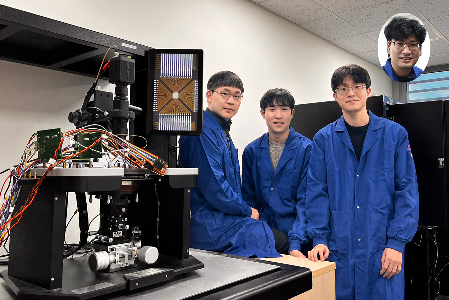 KAIST Develops Neuromorphic Semiconductor Chip that Learns and Corrects Itself
< Photo. The research team of the School of Electrical Engineering posed by the newly deveoped processor. (From center to the right) Professor Young-Gyu Yoon, Integrated Master's and Doctoral Program Students Seungjae Han and Hakcheon Jeong and Professor Shinhyun Choi >
- Professor Shinhyun Choi and Professor Young-Gyu Yoon’s Joint Research Team from the School of Electrical Engineering developed a computing chip that can learn, correct errors, and process AI tasks
- Equipping a computing chip with high-reliability memristor devices with self-error correction functions for real-time learning and image processing
Existing computer systems have separate data processing and storage devices, making them inefficient for processing complex data like AI. A KAIST research team has developed a memristor-based integrated system similar to the way our brain processes information. It is now ready for application in various devices including smart security cameras, allowing them to recognize suspicious activity immediately without having to rely on remote cloud servers, and medical devices with which it can help analyze health data in real time.
KAIST (President Kwang Hyung Lee) announced on the 17th of January that the joint research team of Professor Shinhyun Choi and Professor Young-Gyu Yoon of the School of Electrical Engineering has developed a next-generation neuromorphic semiconductor-based ultra-small computing chip that can learn and correct errors on its own.
< Figure 1. Scanning electron microscope (SEM) image of a computing chip equipped with a highly reliable selector-less 32×32 memristor crossbar array (left). Hardware system developed for real-time artificial intelligence implementation (right). >
What is special about this computing chip is that it can learn and correct errors that occur due to non-ideal characteristics that were difficult to solve in existing neuromorphic devices. For example, when processing a video stream, the chip learns to automatically separate a moving object from the background, and it becomes better at this task over time.
This self-learning ability has been proven by achieving accuracy comparable to ideal computer simulations in real-time image processing. The research team's main achievement is that it has completed a system that is both reliable and practical, beyond the development of brain-like components.
The research team has developed the world's first memristor-based integrated system that can adapt to immediate environmental changes, and has presented an innovative solution that overcomes the limitations of existing technology.
< Figure 2. Background and foreground separation results of an image containing non-ideal characteristics of memristor devices (left). Real-time image separation results through on-device learning using the memristor computing chip developed by our research team (right). >
At the heart of this innovation is a next-generation semiconductor device called a memristor*. The variable resistance characteristics of this device can replace the role of synapses in neural networks, and by utilizing it, data storage and computation can be performed simultaneously, just like our brain cells.
*Memristor: A compound word of memory and resistor, next-generation electrical device whose resistance value is determined by the amount and direction of charge that has flowed between the two terminals in the past.
The research team designed a highly reliable memristor that can precisely control resistance changes and developed an efficient system that excludes complex compensation processes through self-learning. This study is significant in that it experimentally verified the commercialization possibility of a next-generation neuromorphic semiconductor-based integrated system that supports real-time learning and inference.
This technology will revolutionize the way artificial intelligence is used in everyday devices, allowing AI tasks to be processed locally without relying on remote cloud servers, making them faster, more privacy-protected, and more energy-efficient.
“This system is like a smart workspace where everything is within arm’s reach instead of having to go back and forth between desks and file cabinets,” explained KAIST researchers Hakcheon Jeong and Seungjae Han, who led the development of this technology. “This is similar to the way our brain processes information, where everything is processed efficiently at once at one spot.”
The research was conducted with Hakcheon Jeong and Seungjae Han, the students of Integrated Master's and Doctoral Program at KAIST School of Electrical Engineering being the co-first authors, the results of which was published online in the international academic journal, Nature Electronics, on January 8, 2025.
*Paper title: Self-supervised video processing with self-calibration on an analogue computing platform based on a selector-less memristor array ( https://doi.org/10.1038/s41928-024-01318-6 )
This research was supported by the Next-Generation Intelligent Semiconductor Technology Development Project, Excellent New Researcher Project and PIM AI Semiconductor Core Technology Development Project of the National Research Foundation of Korea, and the Electronics and Telecommunications Research Institute Research and Development Support Project of the Institute of Information & communications Technology Planning & Evaluation.
2025.01.17 View 7781
KAIST Develops Neuromorphic Semiconductor Chip that Learns and Corrects Itself
< Photo. The research team of the School of Electrical Engineering posed by the newly deveoped processor. (From center to the right) Professor Young-Gyu Yoon, Integrated Master's and Doctoral Program Students Seungjae Han and Hakcheon Jeong and Professor Shinhyun Choi >
- Professor Shinhyun Choi and Professor Young-Gyu Yoon’s Joint Research Team from the School of Electrical Engineering developed a computing chip that can learn, correct errors, and process AI tasks
- Equipping a computing chip with high-reliability memristor devices with self-error correction functions for real-time learning and image processing
Existing computer systems have separate data processing and storage devices, making them inefficient for processing complex data like AI. A KAIST research team has developed a memristor-based integrated system similar to the way our brain processes information. It is now ready for application in various devices including smart security cameras, allowing them to recognize suspicious activity immediately without having to rely on remote cloud servers, and medical devices with which it can help analyze health data in real time.
KAIST (President Kwang Hyung Lee) announced on the 17th of January that the joint research team of Professor Shinhyun Choi and Professor Young-Gyu Yoon of the School of Electrical Engineering has developed a next-generation neuromorphic semiconductor-based ultra-small computing chip that can learn and correct errors on its own.
< Figure 1. Scanning electron microscope (SEM) image of a computing chip equipped with a highly reliable selector-less 32×32 memristor crossbar array (left). Hardware system developed for real-time artificial intelligence implementation (right). >
What is special about this computing chip is that it can learn and correct errors that occur due to non-ideal characteristics that were difficult to solve in existing neuromorphic devices. For example, when processing a video stream, the chip learns to automatically separate a moving object from the background, and it becomes better at this task over time.
This self-learning ability has been proven by achieving accuracy comparable to ideal computer simulations in real-time image processing. The research team's main achievement is that it has completed a system that is both reliable and practical, beyond the development of brain-like components.
The research team has developed the world's first memristor-based integrated system that can adapt to immediate environmental changes, and has presented an innovative solution that overcomes the limitations of existing technology.
< Figure 2. Background and foreground separation results of an image containing non-ideal characteristics of memristor devices (left). Real-time image separation results through on-device learning using the memristor computing chip developed by our research team (right). >
At the heart of this innovation is a next-generation semiconductor device called a memristor*. The variable resistance characteristics of this device can replace the role of synapses in neural networks, and by utilizing it, data storage and computation can be performed simultaneously, just like our brain cells.
*Memristor: A compound word of memory and resistor, next-generation electrical device whose resistance value is determined by the amount and direction of charge that has flowed between the two terminals in the past.
The research team designed a highly reliable memristor that can precisely control resistance changes and developed an efficient system that excludes complex compensation processes through self-learning. This study is significant in that it experimentally verified the commercialization possibility of a next-generation neuromorphic semiconductor-based integrated system that supports real-time learning and inference.
This technology will revolutionize the way artificial intelligence is used in everyday devices, allowing AI tasks to be processed locally without relying on remote cloud servers, making them faster, more privacy-protected, and more energy-efficient.
“This system is like a smart workspace where everything is within arm’s reach instead of having to go back and forth between desks and file cabinets,” explained KAIST researchers Hakcheon Jeong and Seungjae Han, who led the development of this technology. “This is similar to the way our brain processes information, where everything is processed efficiently at once at one spot.”
The research was conducted with Hakcheon Jeong and Seungjae Han, the students of Integrated Master's and Doctoral Program at KAIST School of Electrical Engineering being the co-first authors, the results of which was published online in the international academic journal, Nature Electronics, on January 8, 2025.
*Paper title: Self-supervised video processing with self-calibration on an analogue computing platform based on a selector-less memristor array ( https://doi.org/10.1038/s41928-024-01318-6 )
This research was supported by the Next-Generation Intelligent Semiconductor Technology Development Project, Excellent New Researcher Project and PIM AI Semiconductor Core Technology Development Project of the National Research Foundation of Korea, and the Electronics and Telecommunications Research Institute Research and Development Support Project of the Institute of Information & communications Technology Planning & Evaluation.
2025.01.17 View 7781 -
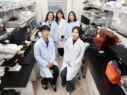 KAIST Research Team Develops Stretchable Microelectrodes Array for Organoid Signal Monitoring
< Photo 1. (From top left) Professor Hyunjoo J. Lee, Dr. Mi-Young Son, Dr. Mi-Ok Lee(In the front row from left) Doctoral student Kiup Kim, Doctoral student Youngsun Lee >
On January 14th, the KAIST research team led by Professor Hyunjoo J. Lee from the School of Electrical Engineering in collaboration with Dr. Mi-Young Son and Dr. Mi-Ok Lee at Korea Research Institute of Bioscience and Biotechnology (KRIBB) announced the development of a highly stretchable microelectrode array (sMEA) designed for non-invasive electrophysiological signal measurement of organoids.
Organoids* are highly promising models for human biology and are expected to replace many animal experiments. Their potential applications include disease modeling, drug screening, and personalized medicine as they closely mimic the structure and function of humans.
*Organoids: three-dimensional in vitro tissue models derived from human stem cells
Despite these advantages, existing organoid research has primarily focused on genetic analysis, with limited studies on organoid functionality. For effective drug evaluation and precise biological research, technology that preserves the three-dimensional structure of organoids while enabling real-time monitoring of their functions is needed. However, it’s challenging to provide non-invasive ways to evaluate the functionalities without incurring damage to the tissues. This challenge is particularly significant for electrophysiological signal measurement in cardiac and brain organoids since the sensor needs to be in direct contact with organoids of varying size and irregular shape. Achieving tight contact between electrodes and the external surface of the organoids without damaging the organoids has been a persistent challenge.
< Figure 1. Schematic image of highly stretchable MEA (sMEA) with protruding microelectrodes. >
The KAIST research team developed a highly stretchable microelectrode array with a unique serpentine structure that contacts the surface of organoids in a highly conformal fashion. They successfully demonstrated real-time measurement and analysis of electrophysiological signals from two types of electrogenic organoids (heart and brain). By employing a micro-electromechanical system (MEMS)-based process, the team fabricated the serpentine-structured microelectrode array and used an electrochemical deposition process to develop PEDOT:PSS-based protruding microelectrodes. These innovations demonstrated exceptional stretchability and close surface adherence to various organoid sizes. The protruding microelectrodes improved contact between organoids and the electrodes, ensuring stable and reliable electrophysiological signal measurements with high signal-to-noise ratios (SNR).
< Figure 2. Conceptual illustration, optical image, and fluorescence images of an organoid captured by the sMEA with protruding microelectrodes.>
Using this technology, the team successfully monitored and analyzed electrophysiological signals from cardiac spheroids of various sizes, revealing three-dimensional signal propagation patterns and identifying changes in signal characteristics according to size. They also measured electrophysiological signals in midbrain organoids, demonstrating the versatility of the technology. Additionally, they monitored signal modulations induced by various drugs, showcasing the potential of this technology for drug screening applications.
< Figure 3. SNR improvement effect by protruding PEDOT:PSS microelectrodes. >
Prof. Hyunjoo Jenny Lee stated, “By integrating MEMS technology and electrochemical deposition techniques, we successfully developed a stretchable microelectrode array adaptable to organoids of diverse sizes and shapes. The high practicality is a major advantage of this system since the fabrication is based on semiconductor fabrication with high volume production, reliability, and accuracy. This technology that enables in situ, real-time analysis of states and functionalities of organoids will be a game changer in high-through drug screening.”
This study led by Ph.D. candidate Kiup Kim from KAIST and Ph.D. candidate Youngsun Lee from KRIBB, with significant contributions from Dr. Kwang Bo Jung, was published online on December 15, 2024 in Advanced Materials (IF: 27.4).
< Figure 4. Drug screening using cardiac spheroids and midbrain organoids.>
This research was supported by a grant from 3D-TissueChip Based Drug Discovery Platform Technology Development Program (No. 20009209) funded by the Ministry of Trade, Industry & Energy (MOTIE, Korea), by the Commercialization Promotion Agency for R&D Outcomes (COMPA) funded by the Ministry of Science and ICT (MSIT) (RS-2024-00415902), by the K-Brain Project of the National Research Foundation (NRF) funded by the Korean government (MSIT) (RS-2023-00262568), by BK21 FOUR (Connected AI Education & Research Program for Industry and Society Innovation, KAIST EE, No. 4120200113769), and by Korea Research Institute of Bioscience and Biotechnology (KRIBB) Research Initiative Program (KGM4722432).
2025.01.14 View 4228
KAIST Research Team Develops Stretchable Microelectrodes Array for Organoid Signal Monitoring
< Photo 1. (From top left) Professor Hyunjoo J. Lee, Dr. Mi-Young Son, Dr. Mi-Ok Lee(In the front row from left) Doctoral student Kiup Kim, Doctoral student Youngsun Lee >
On January 14th, the KAIST research team led by Professor Hyunjoo J. Lee from the School of Electrical Engineering in collaboration with Dr. Mi-Young Son and Dr. Mi-Ok Lee at Korea Research Institute of Bioscience and Biotechnology (KRIBB) announced the development of a highly stretchable microelectrode array (sMEA) designed for non-invasive electrophysiological signal measurement of organoids.
Organoids* are highly promising models for human biology and are expected to replace many animal experiments. Their potential applications include disease modeling, drug screening, and personalized medicine as they closely mimic the structure and function of humans.
*Organoids: three-dimensional in vitro tissue models derived from human stem cells
Despite these advantages, existing organoid research has primarily focused on genetic analysis, with limited studies on organoid functionality. For effective drug evaluation and precise biological research, technology that preserves the three-dimensional structure of organoids while enabling real-time monitoring of their functions is needed. However, it’s challenging to provide non-invasive ways to evaluate the functionalities without incurring damage to the tissues. This challenge is particularly significant for electrophysiological signal measurement in cardiac and brain organoids since the sensor needs to be in direct contact with organoids of varying size and irregular shape. Achieving tight contact between electrodes and the external surface of the organoids without damaging the organoids has been a persistent challenge.
< Figure 1. Schematic image of highly stretchable MEA (sMEA) with protruding microelectrodes. >
The KAIST research team developed a highly stretchable microelectrode array with a unique serpentine structure that contacts the surface of organoids in a highly conformal fashion. They successfully demonstrated real-time measurement and analysis of electrophysiological signals from two types of electrogenic organoids (heart and brain). By employing a micro-electromechanical system (MEMS)-based process, the team fabricated the serpentine-structured microelectrode array and used an electrochemical deposition process to develop PEDOT:PSS-based protruding microelectrodes. These innovations demonstrated exceptional stretchability and close surface adherence to various organoid sizes. The protruding microelectrodes improved contact between organoids and the electrodes, ensuring stable and reliable electrophysiological signal measurements with high signal-to-noise ratios (SNR).
< Figure 2. Conceptual illustration, optical image, and fluorescence images of an organoid captured by the sMEA with protruding microelectrodes.>
Using this technology, the team successfully monitored and analyzed electrophysiological signals from cardiac spheroids of various sizes, revealing three-dimensional signal propagation patterns and identifying changes in signal characteristics according to size. They also measured electrophysiological signals in midbrain organoids, demonstrating the versatility of the technology. Additionally, they monitored signal modulations induced by various drugs, showcasing the potential of this technology for drug screening applications.
< Figure 3. SNR improvement effect by protruding PEDOT:PSS microelectrodes. >
Prof. Hyunjoo Jenny Lee stated, “By integrating MEMS technology and electrochemical deposition techniques, we successfully developed a stretchable microelectrode array adaptable to organoids of diverse sizes and shapes. The high practicality is a major advantage of this system since the fabrication is based on semiconductor fabrication with high volume production, reliability, and accuracy. This technology that enables in situ, real-time analysis of states and functionalities of organoids will be a game changer in high-through drug screening.”
This study led by Ph.D. candidate Kiup Kim from KAIST and Ph.D. candidate Youngsun Lee from KRIBB, with significant contributions from Dr. Kwang Bo Jung, was published online on December 15, 2024 in Advanced Materials (IF: 27.4).
< Figure 4. Drug screening using cardiac spheroids and midbrain organoids.>
This research was supported by a grant from 3D-TissueChip Based Drug Discovery Platform Technology Development Program (No. 20009209) funded by the Ministry of Trade, Industry & Energy (MOTIE, Korea), by the Commercialization Promotion Agency for R&D Outcomes (COMPA) funded by the Ministry of Science and ICT (MSIT) (RS-2024-00415902), by the K-Brain Project of the National Research Foundation (NRF) funded by the Korean government (MSIT) (RS-2023-00262568), by BK21 FOUR (Connected AI Education & Research Program for Industry and Society Innovation, KAIST EE, No. 4120200113769), and by Korea Research Institute of Bioscience and Biotechnology (KRIBB) Research Initiative Program (KGM4722432).
2025.01.14 View 4228 -
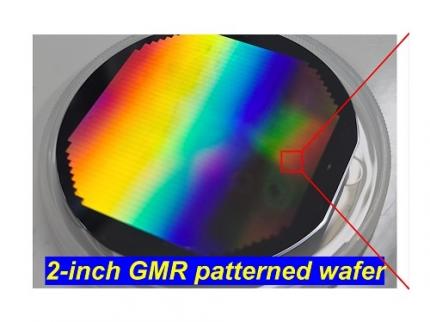 KAIST Secures Core Technology for Ultra-High-Resolution Image Sensors
A joint research team from Korea and the United States has developed next-generation, high-resolution image sensor technology with higher power efficiency and a smaller size compared to existing sensors. Notably, they have secured foundational technology for ultra-high-resolution shortwave infrared (SWIR) image sensors, an area currently dominated by Sony, paving the way for future market entry.
KAIST (represented by President Kwang Hyung Lee) announced on the 20th of November that a research team led by Professor SangHyeon Kim from the School of Electrical Engineering, in collaboration with Inha University and Yale University in the U.S., has developed an ultra-thin broadband photodiode (PD), marking a significant breakthrough in high-performance image sensor technology.
This research drastically improves the trade-off between the absorption layer thickness and quantum efficiency found in conventional photodiode technology. Specifically, it achieved high quantum efficiency of over 70% even in an absorption layer thinner than one micrometer (μm), reducing the thickness of the absorption layer by approximately 70% compared to existing technologies.
A thinner absorption layer simplifies pixel processing, allowing for higher resolution and smoother carrier diffusion, which is advantageous for light carrier acquisition while also reducing the cost. However, a fundamental issue with thinner absorption layers is the reduced absorption of long-wavelength light.
< Figure 1. Schematic diagram of the InGaAs photodiode image sensor integrated on the Guided-Mode Resonance (GMR) structure proposed in this study (left), a photograph of the fabricated wafer, and a scanning electron microscope (SEM) image of the periodic patterns (right) >
The research team introduced a guided-mode resonance (GMR) structure* that enables high-efficiency light absorption across a wide spectral range from 400 nanometers (nm) to 1,700 nanometers (nm). This wavelength range includes not only visible light but also light the SWIR region, making it valuable for various industrial applications.
*Guided-Mode Resonance (GMR) Structure: A concept used in electromagnetics, a phenomenon in which a specific (light) wave resonates (forming a strong electric/magnetic field) at a specific wavelength. Since energy is maximized under these conditions, it has been used to increase antenna or radar efficiency.
The improved performance in the SWIR region is expected to play a significant role in developing next-generation image sensors with increasingly high resolutions. The GMR structure, in particular, holds potential for further enhancing resolution and other performance metrics through hybrid integration and monolithic 3D integration with complementary metal-oxide-semiconductor (CMOS)-based readout integrated circuits (ROIC).
< Figure 2. Benchmark for state-of-the-art InGaAs-based SWIR pixels with simulated EQE lines as a function of TAL variation. Performance is maintained while reducing the absorption layer thickness from 2.1 micrometers or more to 1 micrometer or less while reducing it by 50% to 70% >
The research team has significantly enhanced international competitiveness in low-power devices and ultra-high-resolution imaging technology, opening up possibilities for applications in digital cameras, security systems, medical and industrial image sensors, as well as future ultra-high-resolution sensors for autonomous driving, aerospace, and satellite observation.
Professor Sang Hyun Kim, the lead researcher, commented, “This research demonstrates that significantly higher performance than existing technologies can be achieved even with ultra-thin absorption layers.”
< Figure 3. Top optical microscope image and cross-sectional scanning electron microscope image of the InGaAs photodiode image sensor fabricated on the GMR structure (left). Improved quantum efficiency performance of the ultra-thin image sensor (red) fabricated with the technology proposed in this study (right) >
The results of this research were published on 15th of November, in the prestigious international journal Light: Science & Applications (JCR 2.9%, IF=20.6), with Professor Dae-Myung Geum of Inha University (formerly a KAIST postdoctoral researcher) and Dr. Jinha Lim (currently a postdoctoral researcher at Yale University) as co-first authors. (Paper title: “Highly-efficient (>70%) and Wide-spectral (400 nm -1700 nm) sub-micron-thick InGaAs photodiodes for future high-resolution image sensors”)
This study was supported by the National Research Foundation of Korea.
2024.11.22 View 5888
KAIST Secures Core Technology for Ultra-High-Resolution Image Sensors
A joint research team from Korea and the United States has developed next-generation, high-resolution image sensor technology with higher power efficiency and a smaller size compared to existing sensors. Notably, they have secured foundational technology for ultra-high-resolution shortwave infrared (SWIR) image sensors, an area currently dominated by Sony, paving the way for future market entry.
KAIST (represented by President Kwang Hyung Lee) announced on the 20th of November that a research team led by Professor SangHyeon Kim from the School of Electrical Engineering, in collaboration with Inha University and Yale University in the U.S., has developed an ultra-thin broadband photodiode (PD), marking a significant breakthrough in high-performance image sensor technology.
This research drastically improves the trade-off between the absorption layer thickness and quantum efficiency found in conventional photodiode technology. Specifically, it achieved high quantum efficiency of over 70% even in an absorption layer thinner than one micrometer (μm), reducing the thickness of the absorption layer by approximately 70% compared to existing technologies.
A thinner absorption layer simplifies pixel processing, allowing for higher resolution and smoother carrier diffusion, which is advantageous for light carrier acquisition while also reducing the cost. However, a fundamental issue with thinner absorption layers is the reduced absorption of long-wavelength light.
< Figure 1. Schematic diagram of the InGaAs photodiode image sensor integrated on the Guided-Mode Resonance (GMR) structure proposed in this study (left), a photograph of the fabricated wafer, and a scanning electron microscope (SEM) image of the periodic patterns (right) >
The research team introduced a guided-mode resonance (GMR) structure* that enables high-efficiency light absorption across a wide spectral range from 400 nanometers (nm) to 1,700 nanometers (nm). This wavelength range includes not only visible light but also light the SWIR region, making it valuable for various industrial applications.
*Guided-Mode Resonance (GMR) Structure: A concept used in electromagnetics, a phenomenon in which a specific (light) wave resonates (forming a strong electric/magnetic field) at a specific wavelength. Since energy is maximized under these conditions, it has been used to increase antenna or radar efficiency.
The improved performance in the SWIR region is expected to play a significant role in developing next-generation image sensors with increasingly high resolutions. The GMR structure, in particular, holds potential for further enhancing resolution and other performance metrics through hybrid integration and monolithic 3D integration with complementary metal-oxide-semiconductor (CMOS)-based readout integrated circuits (ROIC).
< Figure 2. Benchmark for state-of-the-art InGaAs-based SWIR pixels with simulated EQE lines as a function of TAL variation. Performance is maintained while reducing the absorption layer thickness from 2.1 micrometers or more to 1 micrometer or less while reducing it by 50% to 70% >
The research team has significantly enhanced international competitiveness in low-power devices and ultra-high-resolution imaging technology, opening up possibilities for applications in digital cameras, security systems, medical and industrial image sensors, as well as future ultra-high-resolution sensors for autonomous driving, aerospace, and satellite observation.
Professor Sang Hyun Kim, the lead researcher, commented, “This research demonstrates that significantly higher performance than existing technologies can be achieved even with ultra-thin absorption layers.”
< Figure 3. Top optical microscope image and cross-sectional scanning electron microscope image of the InGaAs photodiode image sensor fabricated on the GMR structure (left). Improved quantum efficiency performance of the ultra-thin image sensor (red) fabricated with the technology proposed in this study (right) >
The results of this research were published on 15th of November, in the prestigious international journal Light: Science & Applications (JCR 2.9%, IF=20.6), with Professor Dae-Myung Geum of Inha University (formerly a KAIST postdoctoral researcher) and Dr. Jinha Lim (currently a postdoctoral researcher at Yale University) as co-first authors. (Paper title: “Highly-efficient (>70%) and Wide-spectral (400 nm -1700 nm) sub-micron-thick InGaAs photodiodes for future high-resolution image sensors”)
This study was supported by the National Research Foundation of Korea.
2024.11.22 View 5888 -
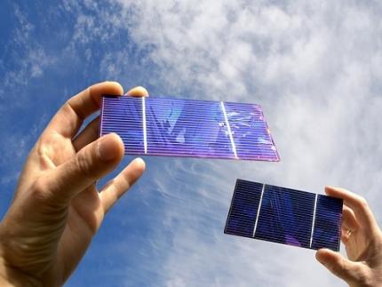 KAIST Researchers Introduce New and Improved, Next-Generation Perovskite Solar Cell
- KAIST-Yonsei university researchers developed innovative dipole technology to maximize near-infrared photon harvesting efficiency
- Overcoming the shortcoming of existing perovskite solar cells that cannot utilize approximately 52% of total solar energy
- Development of next-generation solar cell technology with high efficiency and high stability that can absorb near-infrared light beyond the existing visible light range with a perovskite-dipole-organic semiconductor hybrid structure
< Photo. (From left) Professor Jung-Yong Lee, Ph.D. candidate Min-Ho Lee, and Master’s candidate Min Seok Kim of the School of Electrical Engineering >
Existing perovskite solar cells, which have the problem of not being able to utilize approximately 52% of total solar energy, have been developed by a Korean research team as an innovative technology that maximizes near-infrared light capture performance while greatly improving power conversion efficiency. This greatly increases the possibility of commercializing next-generation solar cells and is expected to contribute to important technological advancements in the global solar cell market.
The research team of Professor Jung-Yong Lee of the School of Electrical Engineering at KAIST (President Kwang-Hyung Lee) and Professor Woojae Kim of the Department of Chemistry at Yonsei University announced on October 31st that they have developed a high-efficiency and high-stability organic-inorganic hybrid solar cell production technology that maximizes near-infrared light capture beyond the existing visible light range.
The research team suggested and advanced a hybrid next-generation device structure with organic photo-semiconductors that complements perovskite materials limited to visible light absorption and expands the absorption range to near-infrared.
In addition, they revealed the electronic structure problem that mainly occurs in the structure and announced a high-performance solar cell device that dramatically solved this problem by introducing a dipole layer*.
*Dipole layer: A thin material layer that controls the energy level within the device to facilitate charge transport and forms an interface potential difference to improve device performance.
Existing lead-based perovskite solar cells have a problem in that their absorption spectrum is limited to the visible light region with a wavelength of 850 nanometers (nm) or less, which prevents them from utilizing approximately 52% of the total solar energy.
To solve this problem, the research team designed a hybrid device that combined an organic bulk heterojunction (BHJ) with perovskite and implemented a solar cell that can absorb up to the near-infrared region.
In particular, by introducing a sub-nanometer dipole interface layer, they succeeded in alleviating the energy barrier between the perovskite and the organic bulk heterojunction (BHJ), suppressing charge accumulation, maximizing the contribution to the near-infrared, and improving the current density (JSC) to 4.9 mA/cm².
The key achievement of this study is that the power conversion efficiency (PCE) of the hybrid device has been significantly increased from 20.4% to 24.0%. In particular, this study achieved a high internal quantum efficiency (IQE) compared to previous studies, reaching 78% in the near-infrared region.
< Figure. The illustration of the mechanism of improving the electronic structure and charge transfer capability through Perovskite/organic hybrid device structure and dipole interfacial layers (DILs). The proposed dipole interfacial layer forms a strong interfacial dipole, effectively reducing the energy barrier between the perovskite and organic bulk heterojunction (BHJ), and suppressing hole accumulation. This technology improves near-infrared photon harvesting and charge transfer, and as a result, the power conversion efficiency of the solar cell increases to 24.0%. In addition, it achieves excellent stability by maintaining performance for 1,200 hours even in an extremely humid environment. >
In addition, this device showed high stability, showing excellent results of maintaining more than 80% of the initial efficiency in the maximum output tracking for more than 800 hours even under extreme humidity conditions.
Professor Jung-Yong Lee said, “Through this study, we have effectively solved the charge accumulation and energy band mismatch problems faced by existing perovskite/organic hybrid solar cells, and we will be able to significantly improve the power conversion efficiency while maximizing the near-infrared light capture performance, which will be a new breakthrough that can solve the mechanical-chemical stability problems of existing perovskites and overcome the optical limitations.”
This study, in which KAIST School of Electrical Engineering Ph.D. candidate Min-Ho Lee and Master's candidate Min Seok Kim participated as co-first authors, was published in the September 30th online edition of the international academic journal Advanced Materials. (Paper title: Suppressing Hole Accumulation Through Sub-Nanometer Dipole Interfaces in Hybrid Perovskite/Organic Solar Cells for Boosting Near-Infrared Photon Harvesting).
This study was conducted with the support of the National Research Foundation of Korea.
2024.10.31 View 7058
KAIST Researchers Introduce New and Improved, Next-Generation Perovskite Solar Cell
- KAIST-Yonsei university researchers developed innovative dipole technology to maximize near-infrared photon harvesting efficiency
- Overcoming the shortcoming of existing perovskite solar cells that cannot utilize approximately 52% of total solar energy
- Development of next-generation solar cell technology with high efficiency and high stability that can absorb near-infrared light beyond the existing visible light range with a perovskite-dipole-organic semiconductor hybrid structure
< Photo. (From left) Professor Jung-Yong Lee, Ph.D. candidate Min-Ho Lee, and Master’s candidate Min Seok Kim of the School of Electrical Engineering >
Existing perovskite solar cells, which have the problem of not being able to utilize approximately 52% of total solar energy, have been developed by a Korean research team as an innovative technology that maximizes near-infrared light capture performance while greatly improving power conversion efficiency. This greatly increases the possibility of commercializing next-generation solar cells and is expected to contribute to important technological advancements in the global solar cell market.
The research team of Professor Jung-Yong Lee of the School of Electrical Engineering at KAIST (President Kwang-Hyung Lee) and Professor Woojae Kim of the Department of Chemistry at Yonsei University announced on October 31st that they have developed a high-efficiency and high-stability organic-inorganic hybrid solar cell production technology that maximizes near-infrared light capture beyond the existing visible light range.
The research team suggested and advanced a hybrid next-generation device structure with organic photo-semiconductors that complements perovskite materials limited to visible light absorption and expands the absorption range to near-infrared.
In addition, they revealed the electronic structure problem that mainly occurs in the structure and announced a high-performance solar cell device that dramatically solved this problem by introducing a dipole layer*.
*Dipole layer: A thin material layer that controls the energy level within the device to facilitate charge transport and forms an interface potential difference to improve device performance.
Existing lead-based perovskite solar cells have a problem in that their absorption spectrum is limited to the visible light region with a wavelength of 850 nanometers (nm) or less, which prevents them from utilizing approximately 52% of the total solar energy.
To solve this problem, the research team designed a hybrid device that combined an organic bulk heterojunction (BHJ) with perovskite and implemented a solar cell that can absorb up to the near-infrared region.
In particular, by introducing a sub-nanometer dipole interface layer, they succeeded in alleviating the energy barrier between the perovskite and the organic bulk heterojunction (BHJ), suppressing charge accumulation, maximizing the contribution to the near-infrared, and improving the current density (JSC) to 4.9 mA/cm².
The key achievement of this study is that the power conversion efficiency (PCE) of the hybrid device has been significantly increased from 20.4% to 24.0%. In particular, this study achieved a high internal quantum efficiency (IQE) compared to previous studies, reaching 78% in the near-infrared region.
< Figure. The illustration of the mechanism of improving the electronic structure and charge transfer capability through Perovskite/organic hybrid device structure and dipole interfacial layers (DILs). The proposed dipole interfacial layer forms a strong interfacial dipole, effectively reducing the energy barrier between the perovskite and organic bulk heterojunction (BHJ), and suppressing hole accumulation. This technology improves near-infrared photon harvesting and charge transfer, and as a result, the power conversion efficiency of the solar cell increases to 24.0%. In addition, it achieves excellent stability by maintaining performance for 1,200 hours even in an extremely humid environment. >
In addition, this device showed high stability, showing excellent results of maintaining more than 80% of the initial efficiency in the maximum output tracking for more than 800 hours even under extreme humidity conditions.
Professor Jung-Yong Lee said, “Through this study, we have effectively solved the charge accumulation and energy band mismatch problems faced by existing perovskite/organic hybrid solar cells, and we will be able to significantly improve the power conversion efficiency while maximizing the near-infrared light capture performance, which will be a new breakthrough that can solve the mechanical-chemical stability problems of existing perovskites and overcome the optical limitations.”
This study, in which KAIST School of Electrical Engineering Ph.D. candidate Min-Ho Lee and Master's candidate Min Seok Kim participated as co-first authors, was published in the September 30th online edition of the international academic journal Advanced Materials. (Paper title: Suppressing Hole Accumulation Through Sub-Nanometer Dipole Interfaces in Hybrid Perovskite/Organic Solar Cells for Boosting Near-Infrared Photon Harvesting).
This study was conducted with the support of the National Research Foundation of Korea.
2024.10.31 View 7058