research
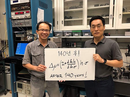
(Professor Shin and Dr. Gunawan (left))
An IBM-KAIST research team described a breakthrough in a 140-year-old mystery in physics. The research reported in Nature last month unlocks the physical characteristics of semiconductors in much greater detail and aids in the development of new and improved semiconductor materials.
Research team under Professor Byungha Shin at the Department of Material Sciences and Engineering and Dr. Oki Gunawan at IBM discovered a new formula and technique that enables the simultaneous extraction of both majority and minority carrier information such as their density and mobility, as well as gain additional insights about carrier lifetimes, diffusion lengths, and the recombination process. This new discovery and technology will help push semiconductor advances in both existing and emerging technologies.
Semiconductors are the basic building blocks of today’s digital electronics age, providing us with a multitude of devices that benefit our modern life. To truly appreciate the physics of semiconductors, it is very important to understand the fundamental properties of the charge carriers inside the materials, whether those particles are positive or negative, their speed under an applied electric field, and how densely they are packed into the material.
Physicist Edwin Hall found a way to determine those properties in 1879, when he discovered that a magnetic field will deflect the movement of electronic charges inside a conductor and that the amount of deflection can be measured as a voltage perpendicular to the flow of the charge. Decades after Hall’s discovery, researchers also recognized that they can measure the Hall effect with light via “photo-Hall experiments”. During such experiments, the light generates multiple carriers or electron–hole pairs in the semiconductors.
Unfortunately, the basic Hall effect only provided insights into the dominant charge carrier (or majority carrier). Researchers were unable to extract the properties of both carriers (the majority and minority carriers) simultaneously. The property information of both carriers is crucial for many applications that involve light such as solar cells and other optoelectronic devices.
In the photo-Hall experiment by the KAIST-IBM team, both carriers contribute to changes in conductivity and the Hall coefficient. The key insight comes from measuring the conductivity and Hall coefficient as a function of light intensity. Hidden in the trajectory of the conductivity, the Hall coefficient curve reveals crucial new information: the difference in the mobility of both carriers. As discussed in the paper, this relationship can be expressed elegantly as: Δµ = d (σ²H)/dσ
The research team solved for both majority and minority carrier mobility and density as a function of light intensity, naming the new technique Carrier-Resolved Photo Hall (CRPH) measurement. With known light illumination intensity, the carrier lifetime can be established in a similar way.
Beyond advances in theoretical understanding, advances in experimental techniques were also critical for enabling this breakthrough. The technique requires a clean Hall signal measurement, which can be challenging for materials where the Hall signal is weak due to low mobility or when extra unwanted signals are present, such as under strong light illumination.
The newly developed photo-Hall technique allows the extraction of an astonishing amount of information from semiconductors. In contrast to only three parameters obtained in the classic Hall measurements, this new technique yields up to seven parameters at every tested level of light intensity. These include the mobility of both the electron and hole; their carrier density under light; the recombination lifetime; and the diffusion lengths for electrons, holes, and ambipolar types. All of these can be repeated N times (i.e. the number of light intensity settings used in the experiment).
Professor Shin said, “This novel technology sheds new light on understanding the physical characteristics of semiconductor materials in great detail.” Dr. Gunawan added, “This will will help accelerate the development of next-generation semiconductor technology such as better solar cells, better optoelectronics devices, and new materials and devices for artificial intelligence technology.”
Profile:
Professor Byungha Shin
Department of Materials Science and Engineering
KAIST
byungha@kaist.ac.kr
http://energymatlab.kaist.ac.kr/
- No Data