research
-
research Simple Molecular Reagents to Treat Alzheimer’s Disease
- Researchers report minimalistic principles for designing small molecules with multiple reactivities against dementia. - Sometimes the most complex problems actually have very simple solutions. A group of South Korean researchers reported an efficient and effective redox-based strategy for incorporating multiple functions into simple molecular reagents against neurodegenerative disorders. The team developed redox-active aromatic molecular reagents with a simple structural composition that ca
2020-05-11 -
research Nanomaterials Mimicking Natural Enzymes with Superior Catalytic Activity and Selectivity for Detecting Acetylcholine
(Professor Jinwoo Lee from the Department of Chemical and Biomolecular Engineering) A KAIST research team doped nitrogen and boron into graphene to selectively increase peroxidase-like activity and succeeded in synthesizing a peroxidase-mimicking nanozyme with a low cost and superior catalytic activity. These nanomaterials can be applied for early diagnosis of Alzheimer’s disease. Enzymes are the main catalysts in our body and are widely used in bioassays. In parti
2019-04-30 -
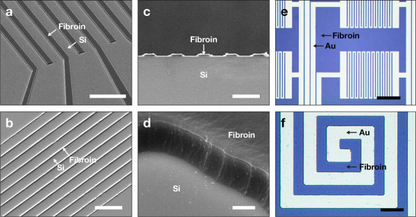
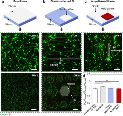
research KAIST Develops Analog Memristive Synapses for Neuromorphic Chips
(Professor Sung-Yool Choi from the School of Electrical Engineering) A KAIST research team developed a technology that makes a transition of the operation mode of flexible memristors to synaptic analog switching by reducing the size of the formed filament. Through this technology, memristors can extend their role to memristive synapses for neuromorphic chips, which will lead to developing soft neuromorphic intelligent systems. Brain-inspired neuromorphic chips have been gaining
2019-02-28 -
research Stretchable Multi-functional Fiber for Energy Harvesting and Strain Sensing
(from left: Professor Steve Park, Jeongjae Ryu and Professor Seungbum Hong) Fiber-based electronics are expected to play a vital role in next-generation wearable electronics. Woven into textiles, they can provide higher durability, comfort, and integrated multi-functionality. A KAIST team has developed a stretchable multi-functional fiber (SMF) that can harvest energy and detect strain, which can be applied to future wearable electronics. With wearable electronics, h
2019-01-31 -
research Fabrication of Shape-conformable Batteries with 3D-Printing
(from left: Dr. Bok Yeop Ahn, Dr. Chanhoon Kim, Professor Il-Doo Kim and Professor Jennifer A. Lewis) Flexible, wireless electronic devices are rapidly emerging and have reached the level of commercialization; nevertheless, most of battery shapes are limited to either spherical and/or rectangular structures, which results in inefficient space use. Professor Il-Doo Kim’s team from the Department of Materials Science at KAIST has successfully developed technology to significantly e
2018-12-20