research

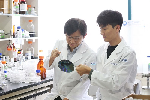
A research team led by Professor Sang Ouk Kim in the Department of Materials Science and Engineering at KAIST has developed semiconductor manufacturing technology using a camera flash.
This technology can manufacture ultra-fine patterns over a large area by irradiating a single flash with a seven-nanometer patterning technique for semiconductors. It can facilitate the manufacturing of highly efficient, integrated semiconductor devices in the future.
Technology for the Artificial Intelligence (AI), the Internet of Things (IoTs), and big data, which are the major keys for the fourth Industrial Revolution, require high-capacity, high-performance semiconductor devices. It is necessary to develop lithography technology to produce such next-generation, highly integrated semiconductor devices.
Although related industries have been using conventional photolithography for small patterns, this technique has limitations for forming a pattern of sub-10 nm patterns.
Molecular assembly patterning technology using polymers has been in the spotlight as the next generation technology to replace photolithography because it is inexpensive to produce and can easily form sub-10 nm patterns. However, since it generally takes a long time for heat treatment at high-temperature or toxic solvent vapor treatment, mass production is difficult and thus its commercialization has been limited.
The research team introduced a camera flash that instantly emits strong light to solve the issues of polymer molecular assembly patterning. Using a flash can possibly achieve a semiconductor patterning of seven nanometers within 15 milliseconds (1 millisecond = 1/1,000 second), which can generate a temperature of several hundred degrees Celsius in several tens of milliseconds.
The team has demonstrated that applying this technology to polymer molecular assembly allows a single flash of light to form molecular assembly patterns.
The team also identified its compatibility with polymer flexible substrates, which are impossible to process at high temperatures. Through these findings, the technology can be applied to the fabrication of next-generation, flexible semiconductors.
The researchers said the camera flash photo-thermal process will be introduced into molecular assembly technology and this highly-efficiency technology can accelerate the realization of molecular assembly semiconductor technology.
Professor Kim, who led the research, said, “Despite its potential, molecular assembly semiconductor technology has remained a big challenge in improving process efficiency.” “This technology will be a breakthrough for the practical use of molecular assembly-based semiconductors.”
The paper was published in the international journal, Advanced Materials on August 21 with first authors, researcher Hyeong Min Jin and PhD candidate Dae Yong Park.
The research, sponsored by the Ministry of Science and ICT, was co-led Professor by Keon Jae Lee in the Department of Materials Science and Engineering at KAIST, and Professor Kwang Ho Kim in the School of Materials Science and Engineering at Pusan National University.
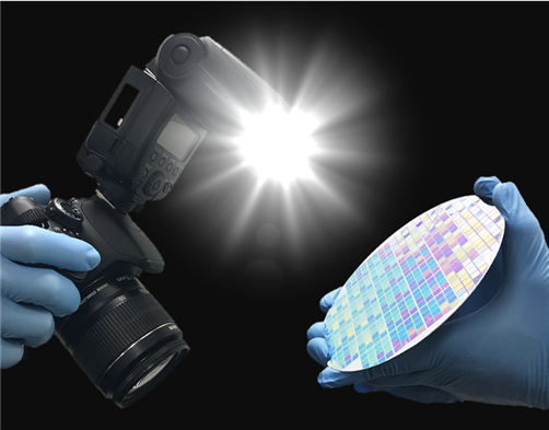
(1. Formation of semiconductor patterns using a camera flash)

(Schematic diagram of molecular assembly pattern using a camera flash)
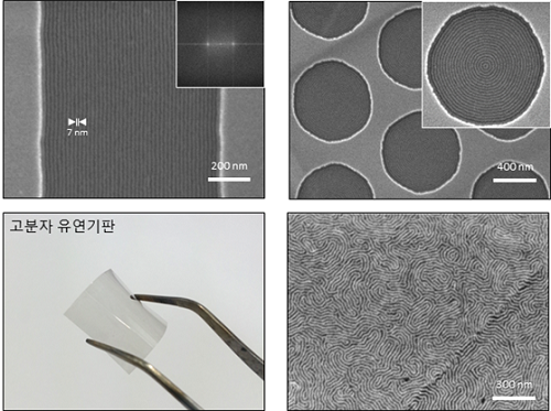
(Self-assembled patterns)
-
research Novel Material Properties of Hybrid Perovskite Nanostructures for Next-generation Non-linear Electronic Devices
(from left: Juho Lee, Dr. Muhammad Ejaz Khan and Professor Yong-Hoon Kim) A KAIST research team reported a novel non-linear device with the founding property coming from perovskite nanowires. They showed that hybrid perovskite-derived, inorganic-framework nanowires can acquire semi-metallicity, and proposed negative differential resistance (NDR) devices with excellent NDR characteristics that resulted from a novel quantum-hybridization NDR mechanism, implying the potential of perovskite nano
2019-02-22 -
research Hierarchical Porous Titanium Nitride Synthesized by Multiscale Phase Separation for LSBs
(from left: Professor Jinwoo Lee and PhD candidate Won-Gwang Lim) A KAIST research team developed ultra-stable, high-rate lithium-sulfur batteries (LSBs) by using hierarchical porous titanium nitride as a sulfur host, and achieved superior cycle stability and high rate performance for LSBs. The control of large amounts of energy is required for use in an electric vehicle or smart grid system. In this sense, the development of next-generation secondary batteries is in high
2019-01-28 -
research Highly Scalable Process to Obtain Stable 2D Nanosheet Dispersion
(Professor Do Hyun Kim and his team) A KAIST team developed technology that allows the mass production of two-dimensional (2D) nanomaterial dispersion by utilizing the characteristic shearing force of hydraulic power. The 2D nanosheet dispersion can be directly applied to solution-based processes to manufacture devices for electronics as well as energy storage and conversion. It is expected to be used in these devices with improved performance. There have been numero
2018-12-19 -
research Characteristics of Submesoscale Geophysical Turbulence Reported
A KAIST research team has reported some of unique characteristics and driving forces behind submesoscale geophysical turbulence. Using big data analysis on ocean surface currents and chlorophyll concentrations observed using coastal radars and satellites has brought better understanding of oceanic processes in space and time scales of O(1) kilometer and O(1) hour. The outcomes of this work will lead to improved tracking of water-borne materials and performance in global and regional climate
2018-12-13 -
research Silk Adhesive Paves the Way for Epidermal Electronics
(from left: Dr. Ji-Won Seo, Professor Hyunjoo Jenny Lee and PhD candidate, Hyojung Kim) Producing effective epidermal electronics requires a strong, biocompatible interface between a biological surface and a sensor. Here, a KAIST team employed a calcium-modified silk fibroin as a biocompatible and strong adhesive. This technology led to the development of epidermal electronics with strong adhesion for patients who need drug injections and physiological monitoring over a long
2018-11-21