research
All matters are made of small particles, namely atoms. An atom is composed of a heavy nucleus and cloud-like, extremely light electrons.
Korean researchers developed an electron microscopy technique that enables the accurate observation of an electron cloud distribution at room-temperature. The achievement is comparable to the invention of the quantum tunneling microscopy technique developed 33 years ago.
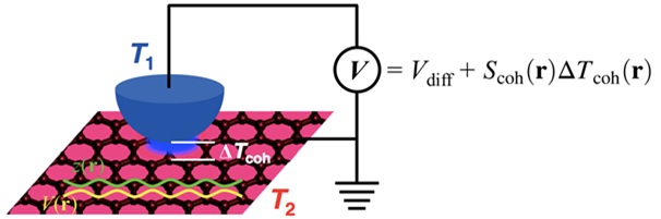
Professor Yong-Hyun Kim of the Graduate School of Nanoscience and Technology at KAIST and Dr. Ho-Gi Yeo of the Korea Research Institute of Standards and Science (KRISS) developed the Scanning Seebeck Microscope (SSM). The SSM renders clear images of atoms, as well as an electron cloud distribution. This was achieved by creating a voltage difference via a temperature gradient.
The development was introduced in the online edition of Physical Review Letters (April 2014), a prestigious journal published by the American Institute of Physics.
The SSM is expected to be economically competitive as it gives high resolution images at an atomic scale even for graphene and semiconductors, both at room temperature. In addition, if the SSM is applied to thermoelectric material research, it will contribute to the development of high-efficiency thermoelectric materials.
Through numerous hypotheses and experiments, scientists now believe that there exists an electron cloud surrounding a nucleus. IBM's Scanning Tunneling Microscope (STM) was the first to observe the electron cloud and has remained as the only technique to this day. The developers of IBM microscope, Dr. Gerd Binnig and Dr. Heinrich Rohrer, were awarded the 1986 Nobel Prize in Physics.
There still remains a downside to the STM technique, however: it required high precision and extreme low temperature and vibration. The application of voltage also affects the electron cloud, resulting in a distorted image.
The KAIST research team adopted a different approach by using the Seebeck effect which refers to the voltage generation due to a temperature gradient between two materials.
The team placed an observation sample (graphene) at room temperature (37~57℃) and detected its voltage generation. This technique made it possible to observe an electron cloud at room temperature.
Furthermore, the research team investigated the theoretical quantum mechanics behind the electron cloud using the observation gained through the Seebeck effect and also obtained by simulation capability to analyze the experimental results.
The research was a joint research project between KAIST Professor Yong-Hyun Kim and KRISS researcher Dr. Ho-Gi Yeo. Eui-Seop Lee, a Ph.D. candidate of KAIST, and KRISS researcher Dr. Sang-Hui Cho also participated. The Ministry of Science, ICT, and Future Planning, the Global Frontier Initiative, and the Disruptive Convergent Technology Development Initiative funded the project in Korea.
Picture 1: Schematic Diagram of the Scanning Seebeck Microscope (SSM)
Picture 2: Electron cloud distribution observed by SSM at room temperature
Picture 3: Professor Yong-Hyun Kim
-
research KAIST's Li-Fi - Achieves 100 Times Faster Speed and Enhanced Security of Wi-Fi
- KAIST-KRISS Develop 'On-Device Encryption Optical Transmitter' Based on Eco-Friendly Quantum Dots - New Li-Fi Platform Technology Achieves High Performance with 17.4% Device Efficiency and 29,000 nit Brightness, Simultaneously Improving Transmission Speed and Security - Presents New Methodology for High-Speed and Encrypted Communication Through Single-Device-Based Dual-Channel Optical Modulation < Photo 1. (Front row from left) Seungmin Shin, First Author; Professor Himchan Cho; (Bac
2025-06-24 -
people OLEV Safety Confirmed by International Standards
On September 19, KAIST announced that the electromagnetic (EM) field levels of its online electric vehicle (OLEV) measured in June and September of this year demonstrated verification of its safety. Last June, the EM field level of OLEV installed at the Seoul Grand Park was measured by the Korea Research Institute of Standards and Science (KRISS) to test its harmfulness to human. The results were 0.5 ~ 61mG which is within the national and international standards of 62.5mG. KRISS measu
2010-09-27