research
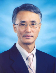
Professor Chang Kee Joo
Professor Kee Joo Chang’s research team from the Department of Physics at KAIST has successfully unearthed the properties of boron and phosphorous dopants in silicon nanowires, a material expected to be used in next generation semiconductors. The research team was the first in the world to investigate the movement of boron and phosphorous (impurities or ‘dopants’ added for electrical flow) in oxidized silicon nanowires and study the mechanism behind its deactivation.
It is nearly impossible to develop a silicon based semiconductor thinner than 10nm, even using the most advanced modern technology. However, the thickness of silicon nanowires are within the nano level and hence, allows a higher degree of integration in semiconductors.
For silicon nanowires to carry electricity, small amounts of boron and phosphorous need to be added (‘doping’ process). Compared to silicon, nanowires are harder to create due to the difficulties in the doping process as well as the control of electrical conduction properties.
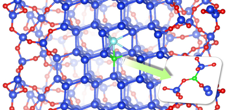
Professor Chang’s research team improved upon the existing simple model by applying revolutionary quantum simulation theory to create a realistic core-shell atomic model. This research successfully investigated the cause of the escape of boron dopants from the silicon core during oxidation. It was also found that although phosphorous dopants do not escape as oxides, they form electrically deactivated pairs which decreases the efficiency. These phenomena were attributed to the film shape of the nano-wires, which increases the relative surface area compared to a same volume of silicon.
The research results were published in the online September edition of the world renowned Nano Letters.
Figure: The longitudinal section diagram of the Silicon/oxide core-shell model
-
research Atomically-Smooth Gold Crystals Help to Compress Light for Nanophotonic Applications
Highly compressed mid-infrared optical waves in a thin dielectric crystal on monocrystalline gold substrate investigated for the first time using a high-resolution scattering-type scanning near-field optical microscope. KAIST researchers and their collaborators at home and abroad have successfully demonstrated a new platform for guiding the compressed light waves in very thin van der Waals crystals. Their method to guide the mid-infrared light with minimal loss will provide a breakthrough f
2022-07-13 -
research Synthesizing Single-Crystalline Hexagonal Graphene Quantum Dots
(Figure: Uniformly ordered single-crystalline graphene quantum dots of various sizes synthesized through solution chemistry.) A KAIST team has designed a novel strategy for synthesizing single-crystalline graphene quantum dots, which emit stable blue light. The research team confirmed that a display made of their synthesized graphene quantum dots successfully emitted blue light with stable electric pressure, reportedly resolving the long-standing challenges of blue light emission in manufa
2019-08-02 -
people KAIST's Doctoral Student Receives a Hoffman Scholarship Award
Hyo-Sun Lee, a doctoral student at the Graduate School of EEWS (Environment, Energy, Water and Sustainability), KAIST, is a recipient of the 2016 Dorothy M. and Earl S. Hoffman Scholarships presented by the American Vacuum Society (AVS). The award ceremony took place during the Society’s 63rd International Symposium and Exhibition on November 6-11, 2016 in Nashville, Tennessee. Lee is the first Korean and foreign student to receive this scholarship. The Hoffman Scholarships were establis
2016-11-17 -
research Anti-Cancer Therapy Delivering Drug to an Entire Tumor Developed
KAIST’s Department of Bio and Brain Engineering Professor Ji-Ho Park and his team successfully developed a new highly efficacious anti-cancer nanotechnology by delivering anti-cancer drugs uniformly to an entire tumor. Their research results were published in Nano Letters online on March 31, 2015. To treat inoperable tumors, anti-cancer medicine is commonly used. However, efficient drug delivery to tumor cells is often difficult, treating an entire tumor with drugs even more so. U
2015-04-07 -
research Development of a Photonic Diode with Light Speed, Single-Direction Transfer
A photonic diode using a nitride semiconductor rod can increase the possibility of developing all-optical integrated circuits, an alternative to conventional integrated circuits. Professor Yong-Hoon Cho's research team from the Department of Physics, KAIST, developed a photonic diode which can selectively transfer light in one way, using semiconductor rods. The photonic diode has a diameter of hundreds of nanometers (nm) and a length of few micrometers. This size enables its use in large-sca
2014-09-23