research
Ultrahigh-resolution displays are an essential element for developing next-generation electronic products such as virtual reality (VR), augmented reality (AR), and smart watches, and can be applied not only to head-mounted displays, but also to smart glasses and smart lenses. The technology developed through this research is expected to be used to make such next-generation ultrahigh-resolution displays and other various sub-micro optoelectronic devices.
KAIST (President Kwang Hyung Lee) announced on the 22nd that Professor Yong-Hoon Cho's research team of KAIST Department of Physics developed the core technology for an ultrahigh resolution light-emitting diode (LED) display that can realize 0.5 micron-scale pixels smaller than 1/100 of the average hair thickness (about 100 microns) using focused ion beams.
Commonly, pixelation of ultrahigh-resolution LED displays usually relies on the etching method that physically cuts the area around the pixel, but as the pixel becomes smaller due to the occurrence of various defects around it, leading to side-effects of having leakage of current increased and light-emission efficiency decreased. In addition, various complex processes such as patterning for pixelation and post-processing for prevention of leakage current are required.
Professor Yong-Hoon Cho's research team developed a technology that can create pixels down to the size of a microscale without the complicated pre- and post-processing using a focused ion beam. This method has the advantage of being able to freely set the shape of the emitting pixel without causing any structural deformation on the material surface by controlling the intensity of the focused ion beam.
The focused ion beam technology has been widely used for ultrahigh-magnification imaging and nanostructure fabrication in fields such as materials engineering and biology. However, when a focused ion beam is used on a light emitting body such as an LED, light emission of a portion hit by the beam and a surrounding area rapidly decreases, which has been a barrier to fabricating a nano-scale light emitting structure. Upon facing this issue, Professor Cho's research team began the research on the idea that if they turned things around to use these problematic phenomena, they can be used in ultra-fine pixelation method on a sub-micron scale.
The research team used a focused ion beam whose intensity was softened to the extent that the surface was not shaved, and found that not only the light-emission rapidly decreased in the area hit by the focused ion beam, but also the local resistance greatly increased. As a result, while the surface of the LED is kept flat, the portion hit by the focused ion beam is optically and electrically isolated, enabling pixelation for independent operation.
Professor Yong-Hoon Cho, who led the research, said, “We have newly developed a technology that can create sub-micron-scale pixels without complicated processes using a focused ion beam, which will be a base technology that can be applied to next-generation ultrahigh-resolution displays and nano-photoelectronic devices.”
This research in which the Master's student Ji-Hwan Moon and the Ph.D. student Baul Kim of KAIST Department of Physics participated as co-first authors, was carried out with the support of the National Research Foundation of Korea's Support Program for Mid-Career Researchers and the Institute of Information and Communications Technology Planning and Evaluation. It was published online in 'Advanced Materials' on February 13, and was also selected as the internal cover of the next offline edition. (Title: Electrically Driven Sub-Micron Light-Emitting Diode Arrays Using Maskless and Etching-Free Pixelation)
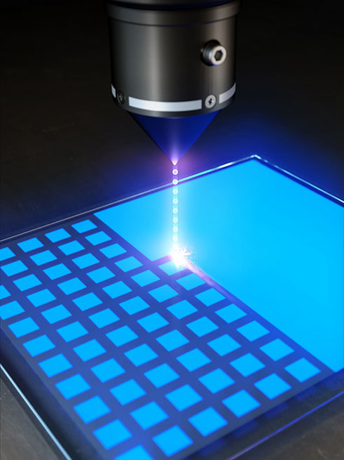
Figure 1. Schematic diagram of the technology for ultrahigh density sub-micron-sized pixels through He focused ion beam (FIB) irradiation on an LED device

Figure 2. Ultra-high-density pixelation technology of micro light-emitting diodes (μLED) through He focused ion beam (FIB) irradiation
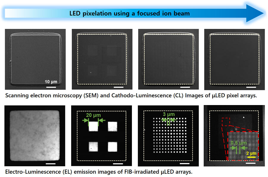
Figure 3. Rectangular pixels of different sizes (surface structure picture and luminescence picture) realized by a focused ion beam. Luminescence pictures of pixel arrays ranging in size from 20 µm x 20 µm to 0.5 µm x 0.5 µm, with surface flatness maintained.