people
President Lee stressed that nurturing medical scientists, semiconductor R&D personnel, startup entrepreneurs, and global innovators are key missions he will continue to pursue during a news conference
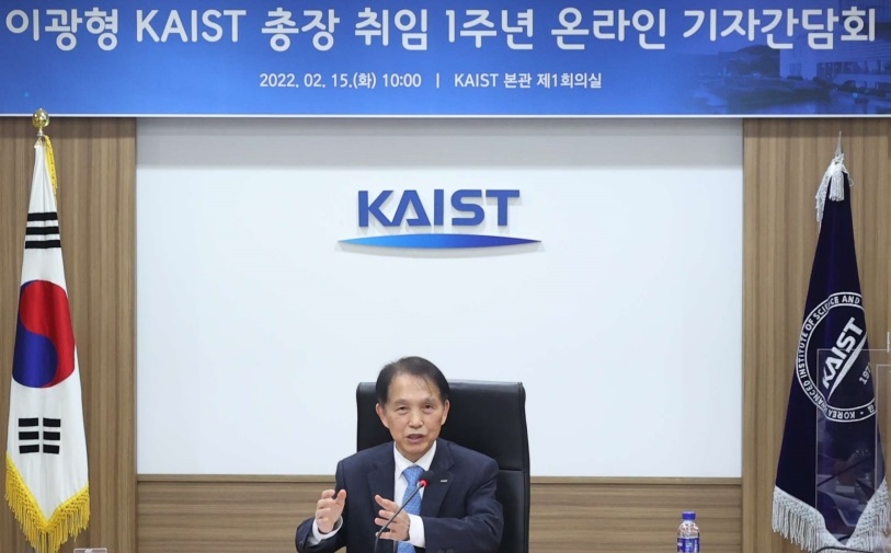
< President Lee holds a news conference marking the 1st anniversary of him becoming the president on February 15. >
KAIST President Kwang Hyung Lee said that nurturing medical scientists, semiconductor R&D personnel, startup entrepreneurs, and global innovators are key missions he will continue to pursue during an online news conference marking the 1st anniversary of him becoming the president on February 15.
He said that nurturing physician-scientists is the most critical mission for KAIST to help the nation create a new growth engine. He said KAIST will help the nation drive the bio-industry and provide medical science resources for the nation’s health sector. To this end, he said that KAIST will open its Medical Science and Technology School by 2026.
“We plan to expand the current Graduate School of Medical Science and Engineering into a new Medical Science and Technology School that will focus entirely on a condensed MD-PhD course converging the fields of AI, bio, and physics,” he said.
The school aims to foster medical scientists whose research results will eventually be commercialized. He said that the university is now discussing revisions to related laws and regulations with the government and other universities.
To supply human resources to the semiconductor industry, President Lee said the university will add a campus in Pyongtaek City that will serve as an advanced convergence research hub in the field of next generation semiconductors in collaboration with Samsung Electronics and the city of Pyongtaek. The three-stage opening plan projected the final opening of the campus by 2036. During the first stage, which will be completed by 2026, it will construct the campus infrastructure in Pyongtaek city where Samsung Semiconductors runs two massive semiconductor complexes. By 2031, it plans to launch the open research platform including a future cities research center and future vehicles research center. The campus will open the global industrial collaboration cluster hub by 2036.
In the global arena, President Lee said he is working to open the New York campus with stakeholders in the United States. He announced the plan last December that was endorsed by New York-based entrepreneur Hee-Nam Bae, the chairman of Big Continent Inc. President Lee and Chairman Lee signed an MOU for the funding to open the campus in New York.
“We are discussing how to facilitate the plan and best accommodate the interests and potential of our students. Many ideas and plans are on the table and we think it will take longer than expected to finalize the plan,” explained President Lee.
However, he added that the basic idea is to offer art tech and health technology programs as well as an AI-based finance MBA at the New York campus, in addition to it serving as the startup accelerator of KAIST.
President Lee stressed the importance of technology commercialization when successfully launching KAIST Holdings last month to help spinoffs of KAIST labs accelerate their end results. He said that KAIST Holdings will build a virtuous supporting system to commercialize the technology startups coming from KAIST.
“We plan to list at least 10 KAIST startups on the KOSDAQ and two on the NASDAQ by 2031. KAIST Holdings also aims to nurture companies valued at a total of one billion KRW and earn 100 billion KRW in technology fees by 2031.
-
research The World’s First Hacking-preventing Cryptographic Semiconductor Chip
With the dramatic increase in the amount of information exchanged between components or devices in the 5G/6G era, such as for the Internet of Things (IoT) and autonomous driving, hacking attacks are becoming more sophisticated. Consequently, enhancing security functions is essential for safely transmitting data between and among devices. On February 29th, a KAIST research team led by Professors Yang-gyu Choi and Seung-tak Ryu from the School of Electrical Engineering announced the successful
2024-03-07 -
research A KAIST research team develops a high-performance modular SSD system semiconductor
In recent years, there has been a rise in demand for large amounts of data to train AI models and, thus, data size has become increasingly important over time. Accordingly, solid state drives (SSDs, storage devices that use a semiconductor memory unit), which are core storage devices for data centers and cloud services, have also seen an increase in demand. However, the internal components of higher performing SSDs have become more tightly coupled, and this tightly-coupled structure limits SSD f
2023-06-23 -
research KAIST develops 'MetaVRain' that realizes vivid 3D real-life images
KAIST (President Kwang Hyung Lee) is a high-speed, low-power artificial intelligence (AI: Artificial Intelligent) semiconductor* MetaVRain, which implements artificial intelligence-based 3D rendering that can render images close to real life on mobile devices. * AI semiconductor: Semiconductor equipped with artificial intelligence processing functions such as recognition, reasoning, learning, and judgment, and implemented with optimized technology based on super intelligence, ultra-low power,
2023-03-13 -
event Shaping the AI Semiconductor Ecosystem
- As the marriage of AI and semiconductor being highlighted as the strategic technology of national enthusiasm, KAIST's achievements in the related fields accumulated through top-class education and research capabilities that surpass that of peer universities around the world are standing far apart from the rest of the pack. As Artificial Intelligence Semiconductor, or a system of semiconductors designed for specifically for highly complicated computation need for AI to conduct its learning a
2022-08-05 -
research Neuromorphic Memory Device Simulates Neurons and Synapses
Simultaneous emulation of neuronal and synaptic properties promotes the development of brain-like artificial intelligence Researchers have reported a nano-sized neuromorphic memory device that emulates neurons and synapses simultaneously in a unit cell, another step toward completing the goal of neuromorphic computing designed to rigorously mimic the human brain with semiconductor devices. Neuromorphic computing aims to realize artificial intelligence (AI) by mimicking the mechanisms of neur
2022-05-20