research
- A KAIST research team led by Professor Keon Jae Lee demonstrates the transfer printing of a large number of micro-sized inorganic semiconductor chips via the selective modulation of micro-vacuum force.
MicroLEDs are a light source for next-generation displays that utilize inorganic LED chips with a size of less than 100 μm. MicroLEDs have attracted a great deal of attention due to their superior electrical/optical properties, reliability, and stability compared to conventional displays such as LCD, OLED, and QD. To commercialize microLEDs, transfer printing technology is essential for rearranging microLED dies from a growth substrate onto the final substrate with a desired layout and precise alignment. However, previous transfer methods still have many challenges such as the need for additional adhesives, misalignment, low transfer yield, and chip damage.
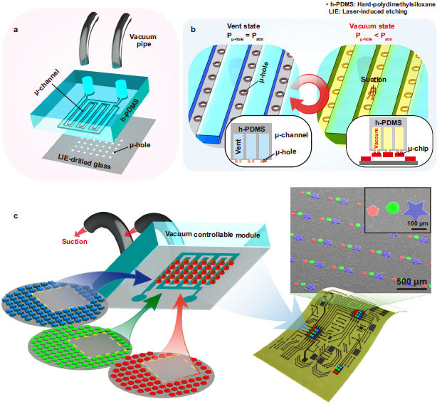
Professor Lee’s research team has developed a micro-vacuum assisted selective transfer printing (µVAST) technology to transfer a large number of microLED chips by adjusting the micro-vacuum suction force.
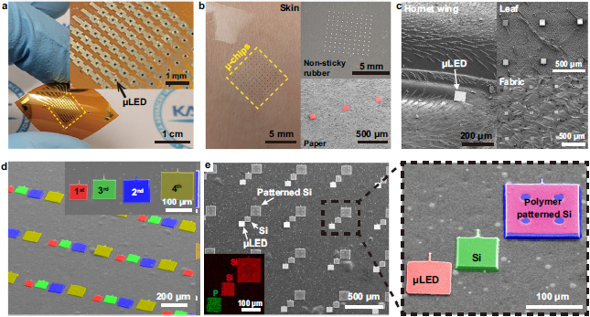
The key technology relies on a laser-induced etching (LIE) method for forming 20 μm-sized micro-hole arrays with a high aspect ratio on glass substrates at fabrication speed of up to 7,000 holes per second. The LIE-drilled glass is connected to the vacuum channels, controlling the micro-vacuum force at desired hole arrays to selectively pick up and release the microLEDs. The micro-vacuum assisted transfer printing accomplishes a higher adhesion switchability compared to previous transfer methods, enabling the assembly of micro-sized semiconductors with various heterogeneous materials, sizes, shapes, and thicknesses onto arbitrary substrates with high transfer yields.

< Figure 01. Concept of micro-vacuum assisted selective transfer printing (μVAST). >
Professor Keon Jae Lee said, “The micro-vacuum assisted transfer provides an interesting tool for large-scale, selective integration of microscale high-performance inorganic semiconductors. Currently, we are investigating the transfer printing of commercial microLED chips with an ejector system for commercializing next-generation displays (Large screen TVs, flexible/stretchable devices) and wearable phototherapy patches.”
This result titled “Universal selective transfer printing via micro-vacuum force” was published in Nature Communications on November 26th, 2023. (DOI: 10.1038/S41467-023-43342-8)

< Figure 02. Universal transfer printing of thin-film semiconductors via μVAST. >

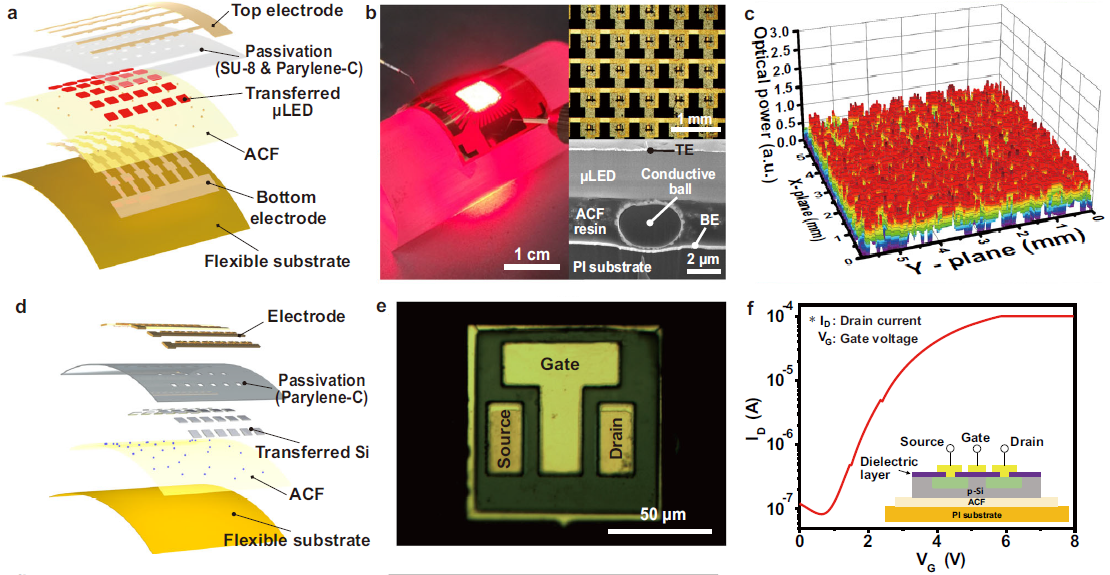
< Figure 03. Flexible devices fabricated by μVAST. >
Title: Entire process including LIE and µVAST
Vimeo link: https://vimeo.com/894430416?share=copy
-
research KAIST Reads the Inside of Materials in 3D Using Everyday LED Light
<(From Left) Professor YongKeun Park, Professor Seung-Mo Hong, Professor Seokwoo Jeon, Ph.D candidate Juheon Lee> KAIST announced on the 7th of May that a research team led by Professor YongKeun Park of the Department of Physics, in collaboration with Professor Seung-Mo Hong’s team at Asan Medical Center and Professor Seokwoo Jeon’s team at Korea University, has developed, for the first time in the world, “incoherent Dielectric Tensor Tomography (iDTT)*,” a techn
2026-05-07 -
research KAIST Solves Computer Problems That Would Take Thousands of Years Using Semiconductors
<(From Left) Professor Yang-Kyu Choi, Ph.D. candidate Seong-Yun Yun, (Upper Right) Professor Sanghyeon Kim, Dr. Joon Pyo Kim> In the era of big data and artificial intelligence, a new approach has emerged for solving combinatorial optimization problems, which involve finding the most efficient solution among many possible options and can otherwise take thousands of years to compute. A KAIST research team has developed computational hardware that can be implemented entirely using existin
2026-05-06 -
research KAIST Develops New Concept Hologram Technology Where “Light Becomes the Key”… Enabling Hard-to-Copy Security
<(From Left)Dr. Joonkyo Jung. Professor Jonghwa Shin> A new type of hologram technology has been developed that uses the motion of light as a “key,” revealing information only under specific conditions. This is gaining attention as a novel approach that can simultaneously overcome the limitations of existing optical communication and security technologies. KAIST (President Kwang Hyung Lee) announced on the 4th of May that a research team led by Professor Jonghwa Shin from t
2026-05-06 -
research KAIST Uncovers the “Core Secret” of Energy Reactions—from Phone Charging to Hydrogen Production
<(From Left) Professor Hyungjun Kim, Ph.D candidate Dong Hyun Kim, Ph.D candidate Minho M. Kim, Ph.D candidate Junsic Cho, Professor Chang Hyuck Choi, Professor Seung-Jae Shin> From smartphone charging to hydrogen production, the fundamental principles of energy technology have been revealed. Korean researchers have, for the first time, identified how molecular structures change within the ultra-small space called the “electric double layer” (a thin interface where the elect
2026-05-04 -
event Professor Hyun Myung Selected for Research Grand Prize at ‘2026 Research Day’
< KAIST Research Day Group Photo > KAIST held the ‘2026 KAIST Research Day’ at the Chung Kunmo Conference Hall in the Academic Cultural Complex at the main Daejeon campus on the morning of the 28th starting at 10:00 AM. ‘Research Day’ is an annual festival for campus researchers that has been held since 2016. It serves as a platform to reward and encourage excellent researchers for their hard work and to exchange R&D information by introducing selected outst
2026-04-30