Nano
-
 Rechargeable Lithium Sulfur Battery for Greater Battery Capacity
Professor Do Kyung Kim from the Department of Material Science and Engineering and Professor Jang Wook Choi from the Graduate School of EEWS have been featured in the lead story of the renowned nanoscience journal Advanced Materials for their research on the lithium sulfur battery. This new type of battery developed by Professor Kim is expected to have a longer life battery life and [higher] energy density than currently commercial batteries.
With ample energy density up to 2100Wh/kg—almost 5.4 times that of lithium ion batteries—lithium sulfur batteries can withstand the sharp decrease in energy capacity resulting from charging and discharging—which has been considered the inherent limitation of the conventional batteries.
Professor Kim and his research team used one-dimensional, vertical alignment of 75nm tick, 15μm long sulfur nanowires to maximize electric conductivity. Then, to prevent loss of battery life, they carbon-coated each nanowire and prohibited direct contact between the sulfur and electrolyte.
The result was one of the most powerful batteries in terms of both energy performance and density. Compared to conventional batteries which suffer from continuous decrease in energy capacity after being discharged, the lithium sulfur battery maintained 99.2% of its initial capacity after being charged and discharged 300 times and up to 70% even after 1000 times.
Professor Kim claims that his new battery is an important step forward towards a high-performance rechargeable battery which is a vital technology for unmanned vehicles, electric automobiles and energy storage. He hopes that his research can solve the problems of battery-capacity loss and contribute to South Korea’s leading position in battery technology. Professor Kim’s research team has filed applications for one domestic and international patent for their research.
2013.12.11 View 14464
Rechargeable Lithium Sulfur Battery for Greater Battery Capacity
Professor Do Kyung Kim from the Department of Material Science and Engineering and Professor Jang Wook Choi from the Graduate School of EEWS have been featured in the lead story of the renowned nanoscience journal Advanced Materials for their research on the lithium sulfur battery. This new type of battery developed by Professor Kim is expected to have a longer life battery life and [higher] energy density than currently commercial batteries.
With ample energy density up to 2100Wh/kg—almost 5.4 times that of lithium ion batteries—lithium sulfur batteries can withstand the sharp decrease in energy capacity resulting from charging and discharging—which has been considered the inherent limitation of the conventional batteries.
Professor Kim and his research team used one-dimensional, vertical alignment of 75nm tick, 15μm long sulfur nanowires to maximize electric conductivity. Then, to prevent loss of battery life, they carbon-coated each nanowire and prohibited direct contact between the sulfur and electrolyte.
The result was one of the most powerful batteries in terms of both energy performance and density. Compared to conventional batteries which suffer from continuous decrease in energy capacity after being discharged, the lithium sulfur battery maintained 99.2% of its initial capacity after being charged and discharged 300 times and up to 70% even after 1000 times.
Professor Kim claims that his new battery is an important step forward towards a high-performance rechargeable battery which is a vital technology for unmanned vehicles, electric automobiles and energy storage. He hopes that his research can solve the problems of battery-capacity loss and contribute to South Korea’s leading position in battery technology. Professor Kim’s research team has filed applications for one domestic and international patent for their research.
2013.12.11 View 14464 -
 Core Technology for Lithium Air Secondary Battery Developed
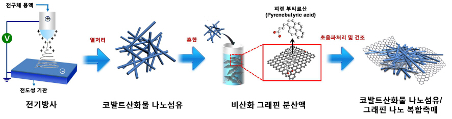
KAIST-Kyonggi University joint research team developed composite catalyst out of nano fiber and graphene
Five times improvement in capacity compared to lithium-ion secondary battery, driving 800 km at maximum
The core technology for lithium air secondary battery, the next generation high capacity battery, has been developed.
A research team formed by KAIST Department of Materials Science’s Professors Il-Doo Kim and Seokwoo Jeon, and Kyonggi University Department of Materials Science’s Professor Yong-Joon Park has created a lithium air secondary battery, with five times greater storage than the lithium-ion secondary battery, by developing a nano fiber-graphene composite catalyst. The research results are published in the August 8th online edition of Nano Letters.
A cathode of a lithium-ion battery consists of graphite and an anode of the battery consists of a lithium transition metal oxide. Lithium-ion batteries are widely used in mobile phones and laptops. However, lithium-ion batteries cannot support electric vehicles, providing energy for only 160 kilometers on one full charge. The lithium air secondary battery just developed by the research team uses lithium on the cathode and oxygen on the anode. It is earning a popular acknowledgement among the next generation secondary battery research community for having lightweight mass and high energy density.
However, lithium-ion batteries remain difficult to commercialize because of their short lifespan. Lithium and oxygen meet up to form lithium oxide (Li2O2) at discharge, and decompose again at charge. In a traditional lithium air battery, this cycle does not occur smoothly and results in high resistance, thereby reducing the lifespan of the battery. It is thus essential to develop high efficiency catalyst that facilitates the formation and decomposition of lithium oxides.
The research team used electric radiation to develop a nano composite catalyst by mixing cobalt oxide nano fiber and graphene. The performance of the battery has been maximized by settling nonoxidative graphene, which has high specific surface area and electrical conductivity, on catalyst active cobalt oxide nano fiber. Applying the nano composite catalyst on both poles of the lithium air battery resulted in an improved lifespan of over 80 recharge cycles with capacity greater than 100mAh/g, five times greater than a lithium ion battery. The newly discovered charge-discharge property is the highest among the reported performances of the lithium air battery so far.
The lithium air battery is cheap to make, as the main materials are metal oxide and graphene. “There are yet more issues to resolve such as stability, but we will collaborate with other organizations to open up the era of electronic vehicles,” said Professor Il-Doo Kim. “We hope to contribute to vitalizing the fields of next generation lithium air battery by leading nanocatalyst synthesis technology, one of the core materials in the fields of secondary battery,” Professor Kim spoke of his aspiration.
The graduate students participated in the research are Won-Hee Ryu, a postdoctorate at KAIST Department of Materials Science, Sungho Song, a PhD candidate at KAIST Department of Materials Science, and Taek-Han Yoon, a graduate student at Kyonggi University.
Picture I: Schematic Diagram of Lithium Air Battery Made of Nano Composite Catalysts
Picture II: Images of Cobalt Oxide Nano Fibers and Graphene Nano Composite Catalysts
Picture III: Images of Manufacturing Process of Cobalt Oxide Nano Fibers and Graphene Nano Composite Catalysts for Lithium Air Battery
2013.10.18 View 13232
Core Technology for Lithium Air Secondary Battery Developed
KAIST-Kyonggi University joint research team developed composite catalyst out of nano fiber and graphene
Five times improvement in capacity compared to lithium-ion secondary battery, driving 800 km at maximum
The core technology for lithium air secondary battery, the next generation high capacity battery, has been developed.
A research team formed by KAIST Department of Materials Science’s Professors Il-Doo Kim and Seokwoo Jeon, and Kyonggi University Department of Materials Science’s Professor Yong-Joon Park has created a lithium air secondary battery, with five times greater storage than the lithium-ion secondary battery, by developing a nano fiber-graphene composite catalyst. The research results are published in the August 8th online edition of Nano Letters.
A cathode of a lithium-ion battery consists of graphite and an anode of the battery consists of a lithium transition metal oxide. Lithium-ion batteries are widely used in mobile phones and laptops. However, lithium-ion batteries cannot support electric vehicles, providing energy for only 160 kilometers on one full charge. The lithium air secondary battery just developed by the research team uses lithium on the cathode and oxygen on the anode. It is earning a popular acknowledgement among the next generation secondary battery research community for having lightweight mass and high energy density.
However, lithium-ion batteries remain difficult to commercialize because of their short lifespan. Lithium and oxygen meet up to form lithium oxide (Li2O2) at discharge, and decompose again at charge. In a traditional lithium air battery, this cycle does not occur smoothly and results in high resistance, thereby reducing the lifespan of the battery. It is thus essential to develop high efficiency catalyst that facilitates the formation and decomposition of lithium oxides.
The research team used electric radiation to develop a nano composite catalyst by mixing cobalt oxide nano fiber and graphene. The performance of the battery has been maximized by settling nonoxidative graphene, which has high specific surface area and electrical conductivity, on catalyst active cobalt oxide nano fiber. Applying the nano composite catalyst on both poles of the lithium air battery resulted in an improved lifespan of over 80 recharge cycles with capacity greater than 100mAh/g, five times greater than a lithium ion battery. The newly discovered charge-discharge property is the highest among the reported performances of the lithium air battery so far.
The lithium air battery is cheap to make, as the main materials are metal oxide and graphene. “There are yet more issues to resolve such as stability, but we will collaborate with other organizations to open up the era of electronic vehicles,” said Professor Il-Doo Kim. “We hope to contribute to vitalizing the fields of next generation lithium air battery by leading nanocatalyst synthesis technology, one of the core materials in the fields of secondary battery,” Professor Kim spoke of his aspiration.
The graduate students participated in the research are Won-Hee Ryu, a postdoctorate at KAIST Department of Materials Science, Sungho Song, a PhD candidate at KAIST Department of Materials Science, and Taek-Han Yoon, a graduate student at Kyonggi University.
Picture I: Schematic Diagram of Lithium Air Battery Made of Nano Composite Catalysts
Picture II: Images of Cobalt Oxide Nano Fibers and Graphene Nano Composite Catalysts
Picture III: Images of Manufacturing Process of Cobalt Oxide Nano Fibers and Graphene Nano Composite Catalysts for Lithium Air Battery
2013.10.18 View 13232 -
 Nanowire Made of Diverse Materials May Become Marketable
- Technology to commercialize nanowire developed after 2 years of industrial-academic joint research -
- 2 million strands of 50nm-width, 20 cm-length nanowire mass producible in 2 hours –
A South Korean joint industrial-academic research team has developed the technology to put forward the commercialization of nanowire that is only a few nanometers wide. It is expected to be applied in various fields such as semiconductors, high performance sensors, and biodevices.
In cooperation with LG Innotek and the National Nanofab center, Professor Jun-Bo Yoon, from KAIST Department of Electrical Engineering, developed the technology to mass produce nanowire at any length with various materials. The research results are published on the online edition of Nano Letters on July 30th.
Nanowire has a long linear structure with its width at 100 nanometers at maximum. It is a multifunctional material that has yet undiscovered thermal, electric, and mechanical properties. Nanowire is highly acclaimed as a cutting-edge material with unique nano-level properties that can be applied in semiconductors, energy, biodevices, and optic devices.
Previously, nanowires had an extremely low synthesis rate that required three or four days to grow few millimeters. It was therefore difficult to produce the desired products using nanowires. Moreover, nanowires needed to be evenly arranged for practical application, but the traditional technology required complex post-treatment, not to mention the arrangement was not immaculate.
The research team applied semiconductor process instead of chemical synthesis to resolve these issues. The team first formed a pattern greater that of the target frequency by using a photo-engraving process on a silicon wafer board whose diameter was 20 centimeters, then repeatedly reduced the frequency to produce 100 nm ultrafine linear grid pattern. Based on this pattern, the research team applied the sputtering process to mass-produce nanowires in perfect shapes of 50 nm width and 20 cm maximum length.
The new technology requires neither a lengthy synthesis process nor post-cleaning to attain a perfectly aligned state. Thus, academic and industrial circles consider the technology has high possibilities for commercialization.
“The significance is in resolving the issues in traditional technology, such as low productivity, long manufacturing time, restrictions in material synthesis, and nanowire alignment,” commented Professor Yoon on this research. “Nanowires have not been widely applied in the industry, but this technology will bring forward the commercialization of high performance semiconductors, optic devices, and biodevices that make use of nanowires.”
2013.10.18 View 10448
Nanowire Made of Diverse Materials May Become Marketable
- Technology to commercialize nanowire developed after 2 years of industrial-academic joint research -
- 2 million strands of 50nm-width, 20 cm-length nanowire mass producible in 2 hours –
A South Korean joint industrial-academic research team has developed the technology to put forward the commercialization of nanowire that is only a few nanometers wide. It is expected to be applied in various fields such as semiconductors, high performance sensors, and biodevices.
In cooperation with LG Innotek and the National Nanofab center, Professor Jun-Bo Yoon, from KAIST Department of Electrical Engineering, developed the technology to mass produce nanowire at any length with various materials. The research results are published on the online edition of Nano Letters on July 30th.
Nanowire has a long linear structure with its width at 100 nanometers at maximum. It is a multifunctional material that has yet undiscovered thermal, electric, and mechanical properties. Nanowire is highly acclaimed as a cutting-edge material with unique nano-level properties that can be applied in semiconductors, energy, biodevices, and optic devices.
Previously, nanowires had an extremely low synthesis rate that required three or four days to grow few millimeters. It was therefore difficult to produce the desired products using nanowires. Moreover, nanowires needed to be evenly arranged for practical application, but the traditional technology required complex post-treatment, not to mention the arrangement was not immaculate.
The research team applied semiconductor process instead of chemical synthesis to resolve these issues. The team first formed a pattern greater that of the target frequency by using a photo-engraving process on a silicon wafer board whose diameter was 20 centimeters, then repeatedly reduced the frequency to produce 100 nm ultrafine linear grid pattern. Based on this pattern, the research team applied the sputtering process to mass-produce nanowires in perfect shapes of 50 nm width and 20 cm maximum length.
The new technology requires neither a lengthy synthesis process nor post-cleaning to attain a perfectly aligned state. Thus, academic and industrial circles consider the technology has high possibilities for commercialization.
“The significance is in resolving the issues in traditional technology, such as low productivity, long manufacturing time, restrictions in material synthesis, and nanowire alignment,” commented Professor Yoon on this research. “Nanowires have not been widely applied in the industry, but this technology will bring forward the commercialization of high performance semiconductors, optic devices, and biodevices that make use of nanowires.”
2013.10.18 View 10448 -
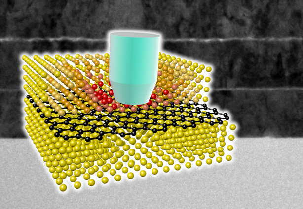 Ultra-High Strength Metamaterial Developed Using Graphene
New metamaterial has been developed, exhibiting hundreds of times greater strength than pure metals.
Professor Seung Min, Han and Yoo Sung, Jeong (Graduate School of Energy, Environment, Water, and Sustainability (EEWS)) and Professor Seok Woo, Jeon (Department of Material Science and Engineering) have developed a composite nanomaterial. The nanomaterial consists of graphene inserted in copper and nickel and exhibits strengths 500 times and 180 times, respectively, greater than that of pure metals. The result of the research was published on the July 2nd online edition in Nature Communications journal.
Graphene displays strengths 200 times greater than that of steel, is stretchable, and is flexible. The U.S. Army Armaments Research, Development and Engineering Center developed a graphene-metal nanomaterial but failed to drastically improve the strength of the material.
To maximize the strength increased by the addition of graphene, the KAIST research team created a layered structure of metal and graphene. Using CVD (Chemical Vapor Deposition), the team grew a single layer of graphene on a metal deposited substrate and then deposited another metal layer. They repeated this process to produce a metal-graphene multilayer composite material, utilizing a single layer of graphene. Micro-compression tests within Transmission Electronic Microscope and Molecular Dynamics simulations effectively showed the strength enhancing effect and the dislocation movement in grain boundaries of graphene on an atomic level.
The mechanical characteristics of the graphene layer within the metal-graphene composite material successfully blocked the dislocations and cracks from external damage from traveling inwards. Therefore the composite material displayed strength beyond conventional metal-metal multilayer materials. The copper-graphene multilayer material with an interplanar distance of 70nm exhibited 500 times greater (1.5GPa) strength than pure copper. Nickel-graphene multilayer material with an interplanar distance of 100nm showed 180 times greater (4.0GPa) strength than pure nickel.
It was found that there is a clear relationship between the interplanar distance and the strength of the multilayer material. A smaller interplanar distance made the dislocation movement more difficult and therefore increased the strength of the material. Professor Han, who led the research, commented, “the result is astounding as 0.00004% in weight of graphene increased the strength of the materials by hundreds of times” and “improvements based on this success, especially mass production with roll-to-roll process or metal sintering process in the production of ultra-high strength, lightweight parts for automobile and spacecraft, may become possible.” In addition, Professor Han mentioned that “the new material can be applied to coating materials for nuclear reactor construction or other structural materials requiring high reliability.”
The research project received support from National Research Foundation, Global Frontier Program, KAIST EEWS-KINC Program and KISTI Supercomputer and was a collaborative effort with KISTI (Korea Institute of Science and Technology Information), KBSI (Korea Basic Science Institute), Stanford University, and Columbia University.
A schematic diagram shows the structure of metal-graphene multi-layers. The metal-graphene multi-layered composite materials, containing a single-layered graphene, block the dislocation movement of graphene layers, resulting in a greater strength in the materials.
2013.08.23 View 18150
Ultra-High Strength Metamaterial Developed Using Graphene
New metamaterial has been developed, exhibiting hundreds of times greater strength than pure metals.
Professor Seung Min, Han and Yoo Sung, Jeong (Graduate School of Energy, Environment, Water, and Sustainability (EEWS)) and Professor Seok Woo, Jeon (Department of Material Science and Engineering) have developed a composite nanomaterial. The nanomaterial consists of graphene inserted in copper and nickel and exhibits strengths 500 times and 180 times, respectively, greater than that of pure metals. The result of the research was published on the July 2nd online edition in Nature Communications journal.
Graphene displays strengths 200 times greater than that of steel, is stretchable, and is flexible. The U.S. Army Armaments Research, Development and Engineering Center developed a graphene-metal nanomaterial but failed to drastically improve the strength of the material.
To maximize the strength increased by the addition of graphene, the KAIST research team created a layered structure of metal and graphene. Using CVD (Chemical Vapor Deposition), the team grew a single layer of graphene on a metal deposited substrate and then deposited another metal layer. They repeated this process to produce a metal-graphene multilayer composite material, utilizing a single layer of graphene. Micro-compression tests within Transmission Electronic Microscope and Molecular Dynamics simulations effectively showed the strength enhancing effect and the dislocation movement in grain boundaries of graphene on an atomic level.
The mechanical characteristics of the graphene layer within the metal-graphene composite material successfully blocked the dislocations and cracks from external damage from traveling inwards. Therefore the composite material displayed strength beyond conventional metal-metal multilayer materials. The copper-graphene multilayer material with an interplanar distance of 70nm exhibited 500 times greater (1.5GPa) strength than pure copper. Nickel-graphene multilayer material with an interplanar distance of 100nm showed 180 times greater (4.0GPa) strength than pure nickel.
It was found that there is a clear relationship between the interplanar distance and the strength of the multilayer material. A smaller interplanar distance made the dislocation movement more difficult and therefore increased the strength of the material. Professor Han, who led the research, commented, “the result is astounding as 0.00004% in weight of graphene increased the strength of the materials by hundreds of times” and “improvements based on this success, especially mass production with roll-to-roll process or metal sintering process in the production of ultra-high strength, lightweight parts for automobile and spacecraft, may become possible.” In addition, Professor Han mentioned that “the new material can be applied to coating materials for nuclear reactor construction or other structural materials requiring high reliability.”
The research project received support from National Research Foundation, Global Frontier Program, KAIST EEWS-KINC Program and KISTI Supercomputer and was a collaborative effort with KISTI (Korea Institute of Science and Technology Information), KBSI (Korea Basic Science Institute), Stanford University, and Columbia University.
A schematic diagram shows the structure of metal-graphene multi-layers. The metal-graphene multi-layered composite materials, containing a single-layered graphene, block the dislocation movement of graphene layers, resulting in a greater strength in the materials.
2013.08.23 View 18150 -
 Nanofiber sensor detects diabetes or lung cancer faster and easier
Metal-oxide nanofiber based chemiresistive gas sensors offer greater usability for portable real-time breath tests that can be available on smart phones or tablet PCs in the near future.
Daejeon, Republic of Korea, June 11, 2013 -- Today"s technological innovation enables smartphone users to diagnose serious diseases such as diabetes or lung cancer quickly and effectively by simply breathing into a small gadget, a nanofiber breathing sensor, mounted on the phones.
Il-Doo Kim, Associate Professor of Materials Science and Engineering Department at the Korea Advanced Institute of Science and Technology (KAIST), and his research team have recently published a cover paper entitled "Thin-Wall Assembled SnO2 Fibers Functionalized by Catalytic Pt Nanoparticles and their Superior Exhaled Breath-Sensing Properties for the Diagnosis of Diabetes," in an academic journal, Advanced Functional Materials (May 20th issue), on the development of a highly sensitive exhaled breath sensor by using hierarchical SnO2 fibers that are assembled from wrinkled thin SnO2 nanotubes.
In the paper, the research team presented a morphological evolution of SnO2 fibers, called micro phase-separations, which takes place between polymers and other dissolved solutes when varying the flow rate of an electrospinning solution feed and applying a subsequent heat treatment afterward.
The morphological change results in nanofibers that are shaped like an open cylinder inside which thin-film SnO2 nanotubes are layered and then rolled up. A number of elongated pores ranging from 10 nanometers (nm) to 500 nm in length along the fiber direction were formed on the surface of the SnO2 fibers, allowing exhaled gas molecules to easily permeate the fibers. The inner and outer wall of SnO2 tubes is evenly coated with catalytic platinum (Pt) nanoparticles. According to the research team, highly porous SnO2 fibers, synthesized by eletrospinning at a high flow rate, showed five-fold higher acetone responses than that of the dense SnO2 nanofibers created under a low flow rate. The catalytic Pt coating shortened the fibers" gas response time dramatically as well.
The breath analysis for diabetes is largely based on an acetone breath test because acetone is one of the specific volatile organic compounds (VOC) produced in the human body to signal the onset of particular diseases. In other words, they are biomarkers to predict certain diseases such as acetone for diabetes, toluene for lung cancer, and ammonia for kidney malfunction. Breath analysis for medical evaluation has attracted much attention because it is less intrusive than conventional medical examination, as well as fast and convenient, and environmentally friendly, leaving almost no biohazard wastes.
Various gas-sensing techniques have been adopted to analyze VOCs including gas chromatography-mass spectroscopy (GC-MS), but these techniques are difficult to incorporate into portable real-time gas sensors because the testing equipment is bulky and expensive, and their operation is more complex. Metal-oxide based chemiresistive gas sensors, however, offer greater usability for portable real-time breath sensors.
Il-Doo Kim said, "Catalyst-loaded metal oxide nanofibers synthesized by electrospinning have a great potential for future exhaled breath sensor applications. From our research, we obtained the results that Pt-coated SnO2 fibers are able to identify promptly and accurately acetone or toluene even at very low concentration less than 100 parts per billion (ppb)."
The exhaled acetone level of diabetes patients exceeds 1.8 parts per million (ppm), which is two to six-fold higher than that (0.3-0.9 ppm) of healthy people. Therefore, a highly sensitive detection that responds to acetone below 1 ppm, in the presence of other exhaled gases as well as under the humid environment of human breath, is important for an accurate diagnosis of diabetes. In addition, Professor Kim said, "a trace concentration of toluene (30 ppb) in exhaled breath is regarded to be a distinctive early symptom of lung cancer, which we were able to detect with our prototype breath tester."
The research team has now been developing an array of breathing sensors using various catalysts and a number of semiconducting metal oxide fibers, which will offer patients a real-time easy diagnosis of diseases.
###
Youtube Link: http://www.youtube.com/watch?v=t_Hr11dRryg
For further inquires:
Il-Doo Kim, Professor of Materials Science and Engineering, KAIST
Advanced Nanomaterials and Energy Laboratory
Tel: +82-42-350-3329
Email: idkim@kaist.ac.kr
Clockwise from left to right: left upper shows a magnified SEM image of a broken thin-wall assembled SnO2 fiber. Left below is an array of breath sensors (Inset is an actual size of a breath sensor). The right is the cover of Advanced Functional Materials (May 20th issue) in which a research paper on the development of a highly sensitive exhaled breath sensor by using SnO2 fibers is published.
This is the microstructural evolution of SnO2 nanofibers as a function of flow rate during electrospinning.
2013.06.20 View 15232
Nanofiber sensor detects diabetes or lung cancer faster and easier
Metal-oxide nanofiber based chemiresistive gas sensors offer greater usability for portable real-time breath tests that can be available on smart phones or tablet PCs in the near future.
Daejeon, Republic of Korea, June 11, 2013 -- Today"s technological innovation enables smartphone users to diagnose serious diseases such as diabetes or lung cancer quickly and effectively by simply breathing into a small gadget, a nanofiber breathing sensor, mounted on the phones.
Il-Doo Kim, Associate Professor of Materials Science and Engineering Department at the Korea Advanced Institute of Science and Technology (KAIST), and his research team have recently published a cover paper entitled "Thin-Wall Assembled SnO2 Fibers Functionalized by Catalytic Pt Nanoparticles and their Superior Exhaled Breath-Sensing Properties for the Diagnosis of Diabetes," in an academic journal, Advanced Functional Materials (May 20th issue), on the development of a highly sensitive exhaled breath sensor by using hierarchical SnO2 fibers that are assembled from wrinkled thin SnO2 nanotubes.
In the paper, the research team presented a morphological evolution of SnO2 fibers, called micro phase-separations, which takes place between polymers and other dissolved solutes when varying the flow rate of an electrospinning solution feed and applying a subsequent heat treatment afterward.
The morphological change results in nanofibers that are shaped like an open cylinder inside which thin-film SnO2 nanotubes are layered and then rolled up. A number of elongated pores ranging from 10 nanometers (nm) to 500 nm in length along the fiber direction were formed on the surface of the SnO2 fibers, allowing exhaled gas molecules to easily permeate the fibers. The inner and outer wall of SnO2 tubes is evenly coated with catalytic platinum (Pt) nanoparticles. According to the research team, highly porous SnO2 fibers, synthesized by eletrospinning at a high flow rate, showed five-fold higher acetone responses than that of the dense SnO2 nanofibers created under a low flow rate. The catalytic Pt coating shortened the fibers" gas response time dramatically as well.
The breath analysis for diabetes is largely based on an acetone breath test because acetone is one of the specific volatile organic compounds (VOC) produced in the human body to signal the onset of particular diseases. In other words, they are biomarkers to predict certain diseases such as acetone for diabetes, toluene for lung cancer, and ammonia for kidney malfunction. Breath analysis for medical evaluation has attracted much attention because it is less intrusive than conventional medical examination, as well as fast and convenient, and environmentally friendly, leaving almost no biohazard wastes.
Various gas-sensing techniques have been adopted to analyze VOCs including gas chromatography-mass spectroscopy (GC-MS), but these techniques are difficult to incorporate into portable real-time gas sensors because the testing equipment is bulky and expensive, and their operation is more complex. Metal-oxide based chemiresistive gas sensors, however, offer greater usability for portable real-time breath sensors.
Il-Doo Kim said, "Catalyst-loaded metal oxide nanofibers synthesized by electrospinning have a great potential for future exhaled breath sensor applications. From our research, we obtained the results that Pt-coated SnO2 fibers are able to identify promptly and accurately acetone or toluene even at very low concentration less than 100 parts per billion (ppb)."
The exhaled acetone level of diabetes patients exceeds 1.8 parts per million (ppm), which is two to six-fold higher than that (0.3-0.9 ppm) of healthy people. Therefore, a highly sensitive detection that responds to acetone below 1 ppm, in the presence of other exhaled gases as well as under the humid environment of human breath, is important for an accurate diagnosis of diabetes. In addition, Professor Kim said, "a trace concentration of toluene (30 ppb) in exhaled breath is regarded to be a distinctive early symptom of lung cancer, which we were able to detect with our prototype breath tester."
The research team has now been developing an array of breathing sensors using various catalysts and a number of semiconducting metal oxide fibers, which will offer patients a real-time easy diagnosis of diseases.
###
Youtube Link: http://www.youtube.com/watch?v=t_Hr11dRryg
For further inquires:
Il-Doo Kim, Professor of Materials Science and Engineering, KAIST
Advanced Nanomaterials and Energy Laboratory
Tel: +82-42-350-3329
Email: idkim@kaist.ac.kr
Clockwise from left to right: left upper shows a magnified SEM image of a broken thin-wall assembled SnO2 fiber. Left below is an array of breath sensors (Inset is an actual size of a breath sensor). The right is the cover of Advanced Functional Materials (May 20th issue) in which a research paper on the development of a highly sensitive exhaled breath sensor by using SnO2 fibers is published.
This is the microstructural evolution of SnO2 nanofibers as a function of flow rate during electrospinning.
2013.06.20 View 15232 -
 Professor Sang-Ouk Kim Interviewed with Arirang TV on April 15, 2013
Professor Sang-Ouk Kim from the Department of Materials Science and Engineering made an appearance on April 15, 2013 at a morning show called “Korea Today” on Arirang TV, an English-language network based in Seoul, South Korea.
Professor Kim introduced his research on the development of flexible semiconductor technology. If commercialized, Professor Kim added, the technology would expedite the common use of wearable computers including mobile devices as well as the development of bio-medical implanted and wireless telemetry bio-devices. To play the video, please click the link below (00:25:00): http://www.arirang.co.kr/Player/TV_Vod.asp?HL=X&code=VOD&vSeq=68872
2013.04.30 View 9974
Professor Sang-Ouk Kim Interviewed with Arirang TV on April 15, 2013
Professor Sang-Ouk Kim from the Department of Materials Science and Engineering made an appearance on April 15, 2013 at a morning show called “Korea Today” on Arirang TV, an English-language network based in Seoul, South Korea.
Professor Kim introduced his research on the development of flexible semiconductor technology. If commercialized, Professor Kim added, the technology would expedite the common use of wearable computers including mobile devices as well as the development of bio-medical implanted and wireless telemetry bio-devices. To play the video, please click the link below (00:25:00): http://www.arirang.co.kr/Player/TV_Vod.asp?HL=X&code=VOD&vSeq=68872
2013.04.30 View 9974 -
 New Technology Will Enable the Commercialization of Plasmon Displays
-- Enhancements in the penetration ratios of color filters are expected by applying nano-surface plasmon effects. --
-- Color filter technology will be applicable to large-area OLED and LCD. --
The fabrication technology to commercialize display color filters using plasmon effects has been discovered.
A joint research team headed by Professor Kyung Cheol Choi from the Department of Electrical Engineering of the Korea Advanced Institute for Science and Technology and Prof. Byeong-Kwon Ju from the School of Electrical Engineering of Korea University has developed the technology to design and produce a display color filter by applying nano-surface plasmon effects.
Color filters are core components used to express colors in CMOS image sensors found in LCD/OLED displays or digital cameras. The current color filters have penetration ratios of 20~30%, but the objective of the joint research team is to raise this penetration ratio by over 40% to facilitate the mass production of energy-efficient plasmonic displays.
Currently available plasmonic color filters are limited to applications on micrometer scales. However, outcomes of the newest research extend the size of the applications up to 2.5 cm by using laser interference lithography. The academic and industrial sectors agree that it is now possible to mass-produce displays using plasmonic color filters.
The researchers built a nanohole array to large scale by using laser interference lithography, a technology that forms nanostructures with laser light interferences. They also suggested a new manufacturing process that can optimize the features of color filters while compensating for defects arising from the fabrication stages.
The new manufacturing process of applying laser interference lithography is expected to overcome the shortcomings of traditional color filters by simplifying production and, enabling them to be produced at lower costs.
“There were limitations to industrial applications of plasmon effect due to production costs, time, and yields,” explained Yun Seon Do, a Ph. D. candidate in the Department of Electrical Engineering of KAIST. “The new technology can reduce fabrication time and cost to the extent that it would be advisable to replace dye-based and pigment-based color filter technology."
“This research can be applied to large-scale displays, such as TV screens, by using laser-interference lithography,” said Jung-Ho Park, a Ph. D. candidate in the School of Electrical Engineering of Korea University. “The research outcome is expected to be widely applied in advanced nano-manufacturing processes as it does not restrict the types of circuit boards."
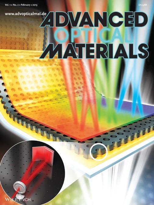
The research outcome, led by doctoral candidates Do and Park, appeared on the front cover of the second issue of Advanced Optical Materials, a highly regarded academic journal in the field of nanotechnologies, and the team has applied for six related patents.
2013.03.13 View 10024
New Technology Will Enable the Commercialization of Plasmon Displays
-- Enhancements in the penetration ratios of color filters are expected by applying nano-surface plasmon effects. --
-- Color filter technology will be applicable to large-area OLED and LCD. --
The fabrication technology to commercialize display color filters using plasmon effects has been discovered.
A joint research team headed by Professor Kyung Cheol Choi from the Department of Electrical Engineering of the Korea Advanced Institute for Science and Technology and Prof. Byeong-Kwon Ju from the School of Electrical Engineering of Korea University has developed the technology to design and produce a display color filter by applying nano-surface plasmon effects.
Color filters are core components used to express colors in CMOS image sensors found in LCD/OLED displays or digital cameras. The current color filters have penetration ratios of 20~30%, but the objective of the joint research team is to raise this penetration ratio by over 40% to facilitate the mass production of energy-efficient plasmonic displays.
Currently available plasmonic color filters are limited to applications on micrometer scales. However, outcomes of the newest research extend the size of the applications up to 2.5 cm by using laser interference lithography. The academic and industrial sectors agree that it is now possible to mass-produce displays using plasmonic color filters.
The researchers built a nanohole array to large scale by using laser interference lithography, a technology that forms nanostructures with laser light interferences. They also suggested a new manufacturing process that can optimize the features of color filters while compensating for defects arising from the fabrication stages.
The new manufacturing process of applying laser interference lithography is expected to overcome the shortcomings of traditional color filters by simplifying production and, enabling them to be produced at lower costs.
“There were limitations to industrial applications of plasmon effect due to production costs, time, and yields,” explained Yun Seon Do, a Ph. D. candidate in the Department of Electrical Engineering of KAIST. “The new technology can reduce fabrication time and cost to the extent that it would be advisable to replace dye-based and pigment-based color filter technology."
“This research can be applied to large-scale displays, such as TV screens, by using laser-interference lithography,” said Jung-Ho Park, a Ph. D. candidate in the School of Electrical Engineering of Korea University. “The research outcome is expected to be widely applied in advanced nano-manufacturing processes as it does not restrict the types of circuit boards."
The research outcome, led by doctoral candidates Do and Park, appeared on the front cover of the second issue of Advanced Optical Materials, a highly regarded academic journal in the field of nanotechnologies, and the team has applied for six related patents.
2013.03.13 View 10024 -
 KAIST welcomes Dr. Sung-Mo
The KAIST Board of Trustees appointed Distinguished Chair Professor Sung-Mo "Steve" Kang of Electrical Engineering at the University of California, Santa Cruz, as the 15th President of KAIST on January 31, 2013. President Kang has begun the duties of his office on February 23, 2013.
An acclaimed scientist, professor, and entrepreneur in the field of integrated-circuit design, Dr. Sung-Mo "Steve" Kang has earned a worldwide reputation for his outstanding research achievements. He led the development of the world’s first full 32-bit CMOS microprocessor chips and their peripheral chips, as well as designed satellite-based private communication networks while working at AT&T Bell Laboratories as a technical supervisor of high-end microprocessor design group (1977-1985).
Dr. Sung-Mo "Steve" Kang served as Chancellor of the University of California, Merced, from 2007 to 2011. During his tenure, he has increased student enrollment, improved the national and international visibility of the university, secured financial resources, expanded faculty and staff, and enhanced campus infrastructure.
Before joining UC Merced, Dr. Kang was Dean of Baskin School of Engineering and Professor of Electrical Engineering during 2001-2007 at UC Santa Cruz where he had initiated several interdisciplinary programs in such areas as biomolecular engineering, information systems and technology management, biomimetic microelectronic systems, quantitative biomedical research, and bioinformatics. He also served as President of Silicon Valley Engineering Council, the alliance for engineering leaders in Silicon Valley (2002-2003).
Dr. Sung-Mo "Steve" Kang was Head of the Department of Electrical and Computer Engineering at the University of Illinois at Urbana-Champaign from 1995 to 2000. He is a fellow of the Institute of Electrical and Electronics Engineers (IEEE), the Association for Computing Machinery (ACM), and the American Association for the Advancement of Science (AAAS), and the president of the IEEE Circuits and Systems Society. Dr. Kang was the founding editor-in-chief of the IEEE Transactions on Very Large Scale Systems (1992-1994).
Dr. Sung-Mo "Steve" Kang holds 15 U.S. patents and has written or co-authored nine books and more than 350 technical papers, and won numerous awards, among others, the Silicon Valley Engineering Hall of Fame (2009), ISQED Quality Award by the International Society for Quality Electronic Design (2008), Chang-Lin Tien Education Leadership Award (2007), IEEE Mac Van Valkenburg Award (2005), and Alexander von Humboldt Award for Senior US Scientists (1997). As an entrepreneur, he co-founded a fabless mobile memory chip design company, ZTI, which is currently located in San Jose, the US.
Dr. Kang earned his doctorate from the University of California, Berkeley; a Master of Science degree from the State University of New York at Buffalo, and a Bachelor of Science degree, graduating summa cum laude, from Fairleigh Dickinson University in Teaneck, NJ. All his academic degrees are in electrical engineering.
2013.02.19 View 12658
KAIST welcomes Dr. Sung-Mo
The KAIST Board of Trustees appointed Distinguished Chair Professor Sung-Mo "Steve" Kang of Electrical Engineering at the University of California, Santa Cruz, as the 15th President of KAIST on January 31, 2013. President Kang has begun the duties of his office on February 23, 2013.
An acclaimed scientist, professor, and entrepreneur in the field of integrated-circuit design, Dr. Sung-Mo "Steve" Kang has earned a worldwide reputation for his outstanding research achievements. He led the development of the world’s first full 32-bit CMOS microprocessor chips and their peripheral chips, as well as designed satellite-based private communication networks while working at AT&T Bell Laboratories as a technical supervisor of high-end microprocessor design group (1977-1985).
Dr. Sung-Mo "Steve" Kang served as Chancellor of the University of California, Merced, from 2007 to 2011. During his tenure, he has increased student enrollment, improved the national and international visibility of the university, secured financial resources, expanded faculty and staff, and enhanced campus infrastructure.
Before joining UC Merced, Dr. Kang was Dean of Baskin School of Engineering and Professor of Electrical Engineering during 2001-2007 at UC Santa Cruz where he had initiated several interdisciplinary programs in such areas as biomolecular engineering, information systems and technology management, biomimetic microelectronic systems, quantitative biomedical research, and bioinformatics. He also served as President of Silicon Valley Engineering Council, the alliance for engineering leaders in Silicon Valley (2002-2003).
Dr. Sung-Mo "Steve" Kang was Head of the Department of Electrical and Computer Engineering at the University of Illinois at Urbana-Champaign from 1995 to 2000. He is a fellow of the Institute of Electrical and Electronics Engineers (IEEE), the Association for Computing Machinery (ACM), and the American Association for the Advancement of Science (AAAS), and the president of the IEEE Circuits and Systems Society. Dr. Kang was the founding editor-in-chief of the IEEE Transactions on Very Large Scale Systems (1992-1994).
Dr. Sung-Mo "Steve" Kang holds 15 U.S. patents and has written or co-authored nine books and more than 350 technical papers, and won numerous awards, among others, the Silicon Valley Engineering Hall of Fame (2009), ISQED Quality Award by the International Society for Quality Electronic Design (2008), Chang-Lin Tien Education Leadership Award (2007), IEEE Mac Van Valkenburg Award (2005), and Alexander von Humboldt Award for Senior US Scientists (1997). As an entrepreneur, he co-founded a fabless mobile memory chip design company, ZTI, which is currently located in San Jose, the US.
Dr. Kang earned his doctorate from the University of California, Berkeley; a Master of Science degree from the State University of New York at Buffalo, and a Bachelor of Science degree, graduating summa cum laude, from Fairleigh Dickinson University in Teaneck, NJ. All his academic degrees are in electrical engineering.
2013.02.19 View 12658 -
 Professor Cho Young-ho wins 'E2 Star' award
Professor Cho Young-ho from the Department of Bio and Brain Engineering at KAIST was chosen as the ‘E2 Star’ at the ‘2012 Engineering Education Festa’ in academics. The ‘2012 Engineering Education Festa’ hosted by the Ministry of Education, Science and Technology was held to display outstanding research results and to conceptualize the future of science education.
The ‘E2 star’ award is given to renowned figures in industry, academia and society. A total of 35 candidates were recommended for the 3 fields and Professor Cho received the first place in the online voting.
Professor Cho received high marks for his work in engineering education, research development and increasing the communication between academia and industry, as well as the commercialization of science and technology. Professor Cho was especially praised for the specialization of engineering education in integrated fields and the joint research with US and Swiss universities.
Professor Cho Young-ho(Department of Bio and Brain Engineering, KAIST)
2012.12.26 View 11955
Professor Cho Young-ho wins 'E2 Star' award
Professor Cho Young-ho from the Department of Bio and Brain Engineering at KAIST was chosen as the ‘E2 Star’ at the ‘2012 Engineering Education Festa’ in academics. The ‘2012 Engineering Education Festa’ hosted by the Ministry of Education, Science and Technology was held to display outstanding research results and to conceptualize the future of science education.
The ‘E2 star’ award is given to renowned figures in industry, academia and society. A total of 35 candidates were recommended for the 3 fields and Professor Cho received the first place in the online voting.
Professor Cho received high marks for his work in engineering education, research development and increasing the communication between academia and industry, as well as the commercialization of science and technology. Professor Cho was especially praised for the specialization of engineering education in integrated fields and the joint research with US and Swiss universities.
Professor Cho Young-ho(Department of Bio and Brain Engineering, KAIST)
2012.12.26 View 11955 -
Firefly inspired high efficiency LED technology developed
A firefly inspired, high efficiency self-illuminating LED has been developed.
Professor Jeong Gi Hoon (Department of Bio and Brain Engineering) mimicked the nanostructure of the external layer of the illumination organ of a firefly and succeeded in fabricating high illumination efficiency LED lenses.
Conventional lenses required expensive anti-reflection coating. The developed lenses utilize the bio-inspired nanostructure on the surface of the lenses themselves to reduce the reflectivity of the lenses thereby decreasing production costs.
The developed antireflection nanostructure is expected to be applied to various digital devices and lighting fixtures.
Antireflective structures have been applied in various fields in order to enhance light efficiency However these structures have been limited to flat surfaces and therefore was difficult to implement to curved surfaces like LED lenses.
Professor Jeong’s team solved this problem by using three dimensional micro molding processes.
The team fabricated the nanostructure by forming a single nanoparticle layer on the silicon oxide and performing dry etching. On this nanostructure PDMS was poured and manipulated to fabricate a lens structure similar to that of a firefly.
The fabricated lens showed similar efficiency as conventional antireflection coating.
2012.11.29 View 9484
-
Principle behind increasing the catalytic property of nanocatalysts proven
The technology that allows full control of the catalytic property of nanocatalysts using oxide formation on nanocatalysts has been developed by KAIST researchers. The breakthrough opens up the possibility of the development of a new kind of catalysts that maximizes catalytic property and minimizes waste.
*nanocatalyst is a material that catalyzes gas reactions on its surface. It is composed of a high surface area oxide scaffold with nano-sized metal particles dispersed.
The team was led by Professor Park Jeong Young of the KAIST EEWS Graduate School and consists of Kamran Qadir Ph.D. candidate (1st Author), Professor Joo Sang Hoon of UNIST, Professor Moon Bong Jin of Hanyang University, and Professor Gabor Somorajai of UC Berkeley. Support for the research was provided from Ministry of Education Science and Technology, National Research Foundation, and Ministry of Knowledge Economy. The results were published as the online edition of Nano Letters: “Intrinsic Relation between Catalytic Activity of CO Oxidation on Ru Nanoparticles and Ru Oxides Uncovered with Ambient Pressure XPS”.
Catalysts are included in above 80% of all the products used in everyday life and are therefore included in most aspects of our lives.
The focus on nanocatalysts is based on finding solutions to increasing the efficiency for application to energy production and for solving environmental issues.
Most nanocatalysts are composed of nanoparticles and oxides where the nanoparticles increase the surface area of the catalyst to increase its activity.
The efficiency of a nanocatalyst is affected by the surface oxide of the nanoparticles. However the proving of this assumption remained difficult to do as it required in-situ measurement of the oxide state of the nanoparticles in the specific environment. Thus far, the experiments were conducted in a vacuum and therefore did not reflect the actual behavior in real life. The recently developed X-ray Photoelectron Spectroscopy allows for measurement of the oxidization state at standard atmospheric pressure.
Professor Park’s research team successfully measured the oxidization state of the nanoparticle using the atmospheric pressure X-ray Photoelectron Spectroscopy in the specified environment.
They confirmed the effect the oxidization state on the catalytic effect of the nanoparticles and additionally found that a thin layer of oxide can increase the catalytic effect and the effectiveness of the nanoparticle can controlled by the oxidation state.
2012.11.29 View 9705
-
Professor Yoon Dong Ki becomes first Korean to Receive the Michi Nakata Prize
Professor Yoon Dong Ki (Graduate School of Nano Science and Technology) became the first Korean to receive the Michi Nakata Prize from the International Liquid Crystal Society.
The Awards Ceremony was held on the 23rd of August in Mainz, Germany in the 24th Annual International Liquid Crystal Conference.
The Michi Nakata Prize was initiated in 2008 and is rewarded every two years to a young scientist that made a ground breaking discovery or experimental result in the field of liquid crystal. Professor Yoon is the first Korean recipient of the Michi Nakata Prize.
Professor Yoon is the founder of the patterning field that utilizes the defect structure formed by smectic displays. He succeeded in large scale patterning complex chiral nano structures that make up bent-core molecules.
Professor Yoon’s experimental accomplishment was published in the Advanced Materials magazine and the Proc. Natl. Acad. Sci. U.S.A. and also as the cover dissertation of Liquid Crystals magazine.
Professor Yoon is currently working on Three Dimensional Nano Patterning of Supermolecular Liquid Crystal and is part of the World Class University organization.
2012.09.11 View 14067