TE
-
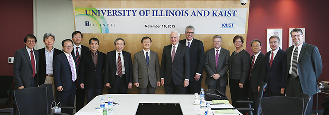 Visit by the President of the University of Illinois at Urbana-Champaign, US
A delegation from the University of Illinois at Urbana-Champaign (UIUC) in the United States visited KAIST on November 11, 2013.
The delegation consisted of senior administrators from the university, the president, vice president for research, dean of engineering college, dean of nursing college, and associate chancellor for corporate and international relations. The managing director of the State of Illinois Far East Office also joined the delegation.
They met with President Steve Kang, including vice presidents and deans of KAIST, and discussed forming a possible partnership between KAIST and UIUC.
Robert A. Easter, the president of UIUC, said, “Higher education institutions today are bearing a critical responsibility to increase the awareness, knowledge, skills, and values needed to create a sustainable future. I hope KAIST and the University of Illinois will join forces to lead innovation in higher education and to stay connected and relevant in a global marketplace.”
President Steve Kang responded, “There would be many opportunities for the two universities to collaborate and achieve global preeminence in such field as biotechnology, engineering, and convergence research.”
The University of Illinois, with three distinct campuses in Chicago, Springfield, and Urbana-Champaign, is one of the most prestigious universities in the world. The university has an annual operating budget of more than USD 5 billion, collectively enrolls more than 78,000 students, awards nearly 20,000 degrees each year, and has more than 665,000 alumni around the world.
2013.11.18 View 8694
 -
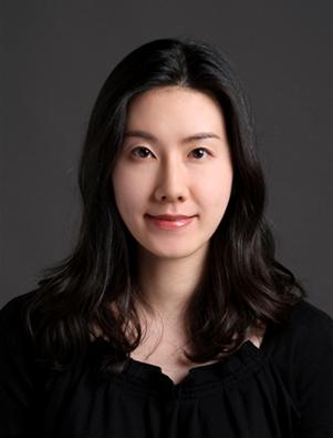 Professor Ji-Yun Lee, Received FAA Recognition Award
Professor Ji-Yun Lee, from the Department of Aerospace Engineering at KAIST, received the US Federal Aviation Administration (FAA) Recognition Award for her Ground-Based Augmentation System (GBAS) and her contribution to the development of satellite navigation technology.
GBAS contributes to the safety of aircraft navigation by providing flawless information with real-time location accuracy within one meter.
Professor Lee developed the monitoring software to improve the safety of GBAS users in her paper published in the International Journal of Radio Science in July of 2012.
The software will be distributed and used by many organizations including Eurocontrol following verification from the FAA technical center. It is expected to be standardized after discussions among international organizations.Professor Lee said, “As satellite navigation is applied to the infrastructure of air, marine, and ground transportation, as well as information & communications and finance, ensuring the performance and safety of the system is the most important factor. GBAS will be further developed and applied as a part of a global service system through international collaboration.”
2013.11.15 View 12734
 -
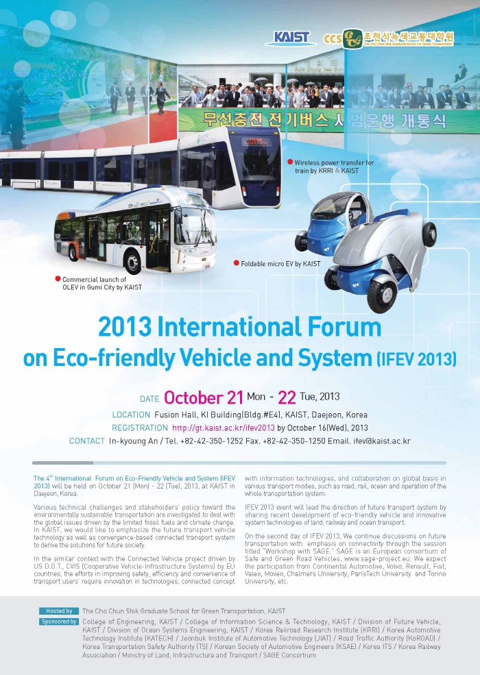 2013 International Forum on Eco-Friendly Vehicle and System
Leaders in transportation technology gathered at KAIST to discuss commercialization & standardization and to encourage the exchange of research progress, strategy, and future initiatives in transportation technology.
The Graduate School for Green Transportation at KAIST hosted the 2013 International Forum on Eco-friendly Vehicles and Systems (IFEV) in Fusion Hall of the KAIST Institute Building from October 21 to 22.
About 50 leaders in the field of future transportation from academic institutes and industries including Dr. Soon-Man Hong, President of Korea Railroad Research Institute (KRRI), Dr. Kwang-Hee Nam, Professor at Pohang University of Science and Technology (POSTECH), and Mr. Mike Schagrin, the Intelligent Transportation Systems Program Manager of the US Department of Transportation (retired) participated in the 4th annual IFEV.
The commercialization & standardization session and a technical session were followed by the plenary meeting of the forum.
Dr. Hong, the keynote speaker, introduced the High Capacity Double Deck High Speed Train, Near Surface Subway System, and Urban Railway System with Wireless Power Transfer Technology under the title “Korea’s Policy and Technology Initiative for Enhancing Green Transport Systems.”
Dr. Kwang-Hee Nam presented “Electric Vehicle Trends & the POSTECH E-Car Research Center Power Train Design,” followed by Mr. Mike Schagrin who spoke about “Going Green with Connected Automation.”
Dr. Omer C. Onar from the Oak Ridge National Laboratory (ORNL) shared recent research on “ORNL Development in Stationary and Dynamic Wireless Charging.”
In the commercialization session, Faical Turki of Vahle, Germany, presented “Wireless Inductive Battery Chargers,” and Professor Kazuyuki Ouchi from Tokyo University presented “Wind Challenger, the Next Generation Hybrid Vessels.”
In the technical session, presentations and discussions were performed on future ground vehicles and railroad technology, intelligent transportation systems and strategy, and policy on eco-friendly vehicle technology, including Professor In-Soo Suh of the Graduate School for Green Transportation at KAIST who presented on “Armadillo-T: 4WD Micro Electric EV with a Foldable Body Concept.”
On the second day of IFEV 2013, representatives of the European Union’s Safe and Green Road Vehicles (SAGE) consortium discussed connectivity in road transportation as a means of improving safety, efficiency and convenience in future safe and green vehicles with collaboration from Korean transportation organizations such as the Korea Transport Institute and Electronics and Telecommunications Research Institute.
Professor Suh, who organized the forum, said, “This forum will serve as an excellent opportunity to discuss and share R&BD progress in the green transportation field. “Details can be found at http://gt.kaist.ac.kr/ifev2013/.
2013.11.15 View 14141
 -
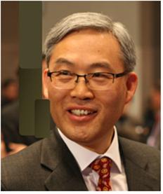 Professor Chun-Taek Rim Appointed as Associate Editor for IEEE TPEL
Professor Chun-Taek Rim of the nuclear and quantum engineering at KAIST was appointed as an associate editor of the Institute of Electrical and Electronics Engineers (IEEE) Transactions on Power Electronics (TPEL), an eminent academic journal bio-monthly published in the field of power electronics.The journal has a high impact factor (4.08), a measure reflecting the average number of citations to recent articles published in an academic journal, which ranks as the 6th the most influential journal among the 100 journals published by IEEE.Professor Rim was also appointed to an associate editor for IEEE Journal of Emerging and Selected Topics in Power Electronics in September in recognition of his expertise in wireless power and electric vehicles.
2013.11.15 View 12132
 -
 KAIST's Partnership Agreement with the Imperial College of Science, Technology and Medicine, UK
KAIST signed an agreement on academic and research cooperation with the Imperial College of Science, Technology (Imperial College London) and Medicine in the United Kingdom (UK) on November 6th, 2013 in London.
The two universities have been implementing collaboration programs at the department level in the areas of plastic electronics since September 2012 and systems engineering and molecular simulation since February 2013, but have never had a formal partnership agreement.
President Steve Kang from KAIST and Provost James Stirling from Imperial College London signed the comprehensive cooperation agreement which will not only strengthen the existing collaborations between the two institutions but also explore areas of mutual interest in the interdisciplinary study of big data, as well as in the fields of mechanical engineering, synthetic biology, and quantum physics.
Workshops, seminars, lectures, and conferences will be jointly organized and held to facilitate the exchange of research staff and faculty and to promote collaborations in research assignments. The universities will also look into the possibility of exchange programs for undergraduate and graduate students.
The partnership agreement will be effective for five years.
Minister Moon-Gi Choi from the Republic of Korea’s Ministry of Science, Information and Communications Technology (ICT) & Future Planning attended the signing ceremony as well and congratulated the establishment of the partnership, saying:
“We are living in the age of highly advanced science and technology that requires us to have a new economic development paradigm for sustainable growth. Through convergence research based on the application of ICT and technology innovation, we will have new opportunities for development. I hope KAIST and the Imperial College London will be at the forefront of such endeavors in coming years.”With its history spanning over 100 years, the Imperial College London is a public research university located in London, UK, specializing in science, engineering, medicine, and business. The university is regarded as being one of the most prestigious universities in the world, having eminent alumni such as Thomas Henry Huxley (biologist), H.G. Wells (author), and Sir Alexander Fleming (pharmacologist).
From left to right: Provost James Stirling, Minister Moon-Gi Choi, and President Steve Kang
2013.11.12 View 10345
 -
 KAIST student wins Aerospace Student Papers Grand Prize
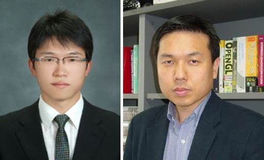
Dong-Il Yoo, a doctoral candidate under Professor Hyun-Chul Shim, at the Department of Aerospace Engineering, KAIST, has been awarded the Second Prize Award at the 11th Korea Aerospace Industries (KAI) Paper Contest. The award ceremony was held on October 30th at the media conference room at the KINTEX ADEX 2013 Exhibition in Seoul.
Yoo"s paper, titled "A Study on Virtual Pursuit Point-based Autonomous Air Combat Guidance Law for UCAV," is highly regarded for originality and creativity. The Field Robotics Center at the KAIST Institute, where Yoo conducted his research, also received the first prize at the 7th KAI Paper Contest.
The KAI Paper Contest was first organized in 2003 to promote academic interest and advance research and development in aerospace engineering among university students.
The KAI Paper Contest is one of the most prestigious contests in Korea. It is sponsored by the Ministry of Trade, Industry and Energy, the Ministry of Land, Infrastructure and Transport, the Korean Society for Aeronautical and Space Sciences, the Korea Aerospace Industries Association, and the Korea Civil Aviation Development Association.
Dong-Il Yoo (left) and Professor Hyun-Chul Shim (right)
2013.11.11 View 14464
 -
 Kinetic Lighting, Dlight, Dominates World Renowned Design Awards
Professor Sang-Min Bae
“D’light,” a lamp that transforms its lampshade shape, developed by a team led by KAIST Department of Industrial Design’s Professor Sang-Min Bae, won Japan’s Good Design Awards on October the 2nd, soon after winning the internationally renowned 2013 International Design Excellence Awards (IDEA) in August.
IDEA, sponsored by the Industrial Design Society of America (IDSA) and BusinessWeek, awards the best work from over 6,000 exhibits from 50 countries. Japan’s Good Design Awards, founded by the Japan Institute of Design Promotion (JDP) in 1957, is the most prestigious and one of the World’s four major design awards.
“D’light” combines “donative” and “light.” Its meaning originates from the meaning of “delight” which means “giving great joy.” The shape and the brightness of the lamp can be transformed by turning the end of the heart-shaped lampshade. The team states that the lamp carries a figurative meaning of generous hearts lighting the neglected of the world by designing the lamp to be the brightest when it takes the shape of a heart. D’light developed as the 5th product of “the Nanum” project that started in 2006. Professor Bae first participated in the project in developing the 2nd product, “Cross Cube” in 2007. The he designed and launched the environmentally friendly humidifier “Lovepot” in 2008 and interactive tumbler “Hearty” in 2009.
The “Nanum” project aims to develop innovative products for charity to create a humane social circulatory system. The project, led by the international relief and development organisation, World Vision and KAIST’s ID+IM laboratory run by Professor Bae, donates all profits to educate the children of low-income families. The project raised a total of 1.7 billion Korean won from 2007 this year to provide scholarships to 240 children in need.
Professor Bae’s team has undertaken seed and “Nanum” projects with the theme of philanthropy design helping people in need by creating innovative designs. The project has produced four excellent and authentic products which received 44 world renowned design awards.
Professor Bae said, “’The Nanum’ project consists of planning, designing, producing and selling for charity and donates all profit to children in need through education and scholarship.” He continued, “The consumers can purchase products that are aesthetically pleasing and convenient as well as gaining an opportunity to donate to children in need.”
Figure1 Kinetic lighting D’light
Figure 2. Characteristics of “Nanum” D’light
The shape of the lampshade can be transformed. The lamp sheds the brightest light when it takes the shape of a heart, hence showing the figurative meaning of brightening the neglected parts of the world with generous hearts.
Figure 3. Detailed Images of D’light
2013.11.11 View 11497
 -
 Observation of a water strider led to a new method of measuring properties of Nano films
Even the mechanical properties of Nano films of a few nanometers thick can be measured
Posted online Nature Communications on the 3rd of October
The joint research team of KAIST’s Department of Mechanical Engineering’s Professor Taek-Soo Kim and Doctor Seung-Min Hyun of the Nano mechanics laboratory of Korea Institute of Machinery and Materials has developed a new method to evaluate mechanical properties of Nano films using the characteristics of water surfaces.
The research findings have been posted on the online edition of Nature Communications on the 3rd of October. The technology can obtain accurate results by directly measuring the mechanical properties such as the strength and elasticity of Nano films. Academia and the industry expect the simplicity of the technology to present a new paradigm in the evaluation of mechanical properties of Nano films.
Evaluation of the mechanical properties of Nano films is essential not only in predicting the reliability of semiconductors and displays, but also in finding new phenomena in the Nano world. However, mechanical strength was difficult to test since the test demands the falling of objects to the ground to measure their strength, and nano films can easily break in the process.
The research team observed insects such as water striders freely floating on the surface of the water. The team used the properties of water, large surface tension and low viscosity, to float a 55 nanometers (nm) gold Nano film to successfully measure its mechanical properties without damaging it. The technology could be used to measure the mechanical properties of not only various types of Nano films but also films only a few nm thick.
Professor Taek-Soo Kim said, “We effectively performed an evaluation of the mechanical characteristics of Nano films, which was difficult in the past, by developing a new strength test using the properties of water.” He continued to say, “The team plans to discover the mechanical properties of 2D Nano films such as graphene that could not have been measured with the existing strength test methods.”
The research by KAIST’s Department of Mechanical Engineering’s graduate student Jae-Han Kim (lead author) under the supervision of Professor Taek-Soo Kim and Doctor Seung-Min Hyun of Korea Institute of Machinery and Materials was sponsored by the National Research Foundation of Korea.
Evaluation process of mechanical properties of Nano films by using the characteristics of water surfaces
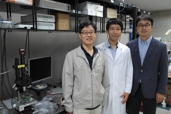
Dr Seung-Min Hyun, Jae-Han Kim, and Professor Taek-Soo Kim from left to right
2013.11.11 View 9903
 -
 The World Economic Forum Invites KAIST to 2014 Davos Forum
President Steve Kang and Distinguished Professor Sang Yup Lee have been invited by the World Economic Forum (WEF) to attend its annual meeting slated for January 22-25, 2014 in Davos-Klosters, Switzerland.
The president will also join the Global University Leaders Forum (GULF) to be held during the annual meeting. The GULF consists of leading research universities throughout the world, at which President Kang will address agenda related to higher education and research.
From September 11th to 13th, KAIST was invited to the WEF’s 2013 Summer Davos Forum held in Dalian, China. The Summer Davos Forum is recognized as a barometer of the world economy, and KAIST hosted three sessions there.
In a session titled “Smart Regulations,” Professor Sang Yup Lee hosted presentations and discussions under the topic of “How regulation models can strengthen technical innovation and expansion.” President Steve Kang, Peter Sands, CEO of Standard Chartered Bank Group, Mark Weinberger, CEO of Ernest & Young, and Peter Terium, CEO of RWE, participated in the discussions.
The KAIST delegates also presented and participated in a session titled “From Trade Center to Innovative Hub” to discuss how to lead innovations in Asia, as well as “Marine Resources: Finding New Frontier” to address issues of how to develop and manage oceanic resources for potential growth.
President Kang said, “The World Economic Forum allows us to introduce the results of our innovative and creative research to global leaders and to demonstrate that our global position continues to grow.”
The WEF has been hosting Summer Davos Forum in China since 2007. About 1,500 participants from over 90 countries joined in this year’s summer forum under the theme of “Innovation: Inevitable Mainstream.” New strategies for innovations and solutions for global threats were suggested through presentations and discussions in 125 sessions.
The World Economic Forum (WEF) is an independent, international, and non-profit organization based in Geneva, Switzerland. It is committed to improving the state of the world by engaging business, political, academic, and government leaders to shape global, regional and industry agenda.
Among the meetings and forums organized by the WEF, its annual meeting held each January in Davos, a.k.a. the Davos Forum, has been the best known gathering. The Davos Forum brings together some 2,500 top business leaders, international political leaders, selected intellectuals and journalists to discuss the most pressing issues facing the world including health and environment.
2013.11.07 View 12531
 -
 Professor Jae-Hyung Lee appointed as AIChE fellow
Professor Jae-Hyung Lee from the Department of Chemical and Bimolecular Engineering at KAIST was appointed as a fellow in the American Institute of Chemical Engineers (AIChE).
Established in 1908, AIChE is the largest association of chemical engineers worldwide, which now boasts more than 40,000 members from 90 countries.
Following Distinguished Professor Sang Yup Lee from the same department at KAIST, Professor Jae-Hyung Lee is the second Korean appointed as a fellow by the organization.
He has been acknowledged for his innovative research on the improvement of model predictive control of industrial processes.
Professor Lee is the director of the Saudi Armaco-KAIST CO2 Management Center at KAIST, a fellow of the Institute of Electrical and Electronics Engineers (IEEE) and the International Federation of Automatic Control (IFAC), and a member of the Korean Academy of Science and Technology.
He received the Young Investigator Award from the National Science Foundation (NSF) in 1994 and the Computing in Chemical Engineering Award from AIChE in 2013.
2013.11.05 View 10913
 -
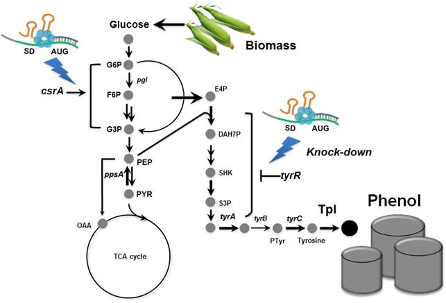 Metabolically engineered E. coli producing phenol
Many chemicals we use in everyday life are derived from fossil resources. Due to the increasing concerns on the use of fossil resources, there has been much interest in producing chemicals from renewable resources through biotechnology.
Phenol is an important commodity chemical, and is a starting material for the production of numerous industrial chemicals and polymers, including bisphenol A and phenolic resins, and others. At present, the production of phenol entirely depends on the chemical synthesis from benzene, and its annual production exceeds 8 million tons worldwide. Microbial production of phenol seems to be a non-viable process considering the high toxicity of phenol to the cell.
In the paper published online in Biotechnology Journal, a Korean research team led by Distinguished Professor Sang Yup Lee at the Department of Chemical and Biomolecular Engineering from the Korea Advanced Institute of Science and Technology (KAIST) reported the successful development of an engineered Escherichia coli (E. coli) strain which can produce phenol from glucose. E. coli has been a workhorse for biological production of various value-added compounds such as succinic acid and 1,4-butanediol in industrial scale. However, due to its low tolerance to phenol, E. coli was not considered a viable host strain for the biological production of phenol.
Professor Lee"s team, a leading research group in metabolic engineering, noted the genetic and physiological differences of various E. coli strains and investigated 18 different E. coli strains with respect to phenol tolerance and engineered all of the 18 strains simultaneously. If the traditional genetic engineering methods were used, this work would have taken years to do. To overcome this challenge, the research team used synthetic small RNA (sRNA) technology they recently developed (Nature Biotechnology, vol 31, pp 170-174, 2013). The sRNA technology allowed the team to screen 18 E. coli strains with respect to the phenol tolerance, and the activities of the metabolic pathway and enzyme involved in the production of phenol. The research team also metabolically engineered the E. coli strains to increase carbon flux toward phenol and finally generated an engineered E. coli strain which can produce phenol from glucose.
Furthermore, the team developed a biphasic extractive fermentation process to minimize the toxicity of phenol to E. coli cells. Glycerol tributyrate was found to have low toxicity to E. coli and allowed efficient extraction of phenol from the culture broth. Through the biphasic fed-batch fermentation using glycerol tributyrate as an in situ extractant, the final engineered E. coli strain produced phenol to the highest titer and productivity reported (3.8 g/L and 0.18 g/L/h, respectively). The strategy used for the strain development and the fermentation process will serve as a framework for metabolic engineering of microorganisms for the production of toxic chemicals from renewable resources.
This work was supported by the Intelligent Synthetic Biology Center through the Global Frontier Project (2011-0031963) of the Ministry of Science, ICT & Future Planning through the National Research Foundation of Korea.
Process of Phenol Production
2013.11.05 View 11550
 -
 KAIST announced a novel technology to produce gasoline by a metabolically engineered microorganism
A major scientific breakthrough in the development of renewable energy sources and other important chemicals; The research team succeeded in producing 580 mg of gasoline per liter of cultured broth by converting in vivo generated fatty acids
For many decades, we have been relying on fossil resources to produce liquid fuels such as gasoline, diesel, and many industrial and consumer chemicals for daily use. However, increasing strains on natural resources as well as environmental issues including global warming have triggered a strong interest in developing sustainable ways to obtain fuels and chemicals.
Gasoline, the petroleum-derived product that is most widely used as a fuel for transportation, is a mixture of hydrocarbons, additives, and blending agents. The hydrocarbons, called alkanes, consist only of carbon and hydrogen atoms. Gasoline has a combination of straight-chain and branched-chain alkanes (hydrocarbons) consisted of 4-12 carbon atoms linked by direct carbon-carbon bonds.
Previously, through metabolic engineering of Escherichia coli (E. coli), there have been a few research results on the production of long-chain alkanes, which consist of 13-17 carbon atoms, suitable for replacing diesel. However, there has been no report on the microbial production of short-chain alkanes, a possible substitute for gasoline.
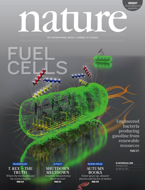
In the paper (entitled "Microbial Production of Short-chain Alkanes") published online in Nature on September 29, a Korean research team led by Distinguished Professor Sang Yup Lee of the Department of Chemical and Biomolecular Engineering at the Korea Advanced Institute of Science and Technology (KAIST) reported, for the first time, the development of a novel strategy for microbial gasoline production through metabolic engineering of E. coli.
The research team engineered the fatty acid metabolism to provide the fatty acid derivatives that are shorter than normal intracellular fatty acid metabolites, and introduced a novel synthetic pathway for the biosynthesis of short-chain alkanes. This allowed the development of platform E. coli strain capable of producing gasoline for the first time. Furthermore, this platform strain, if desired, can be modified to produce other products such as short-chain fatty esters and short-chain fatty alcohols.
In this paper, the Korean researchers described detailed strategies for 1) screening of enzymes associated with the production of fatty acids, 2) engineering of enzymes and fatty acid biosynthetic pathways to concentrate carbon flux towards the short-chain fatty acid production, and 3) converting short-chain fatty acids to their corresponding alkanes (gasoline) by introducing a novel synthetic pathway and optimization of culture conditions. Furthermore, the research team showed the possibility of producing fatty esters and alcohols by introducing responsible enzymes into the same platform strain.
Professor Sang Yup Lee said, "It is only the beginning of the work towards sustainable production of gasoline. The titer is rather low due to the low metabolic flux towards the formation of short-chain fatty acids and their derivatives. We are currently working on increasing the titer, yield and productivity of bio-gasoline. Nonetheless, we are pleased to report, for the first time, the production of gasoline through the metabolic engineering of E. coli, which we hope will serve as a basis for the metabolic engineering of microorganisms to produce fuels and chemicals from renewable resources."
This research was supported by the Advanced Biomass Research and Development Center of Korea (ABC-2010-0029799) through the Global Frontier Research Program of the Ministry of Science, ICT and Future Planning (MSIP) through the National Research Foundation (NRF), Republic of Korea. Systems metabolic engineering work was supported by the Technology Development Program to Solve Climate Changes on Systems Metabolic Engineering for Biorefineries (NRF-2012-C1AAA001-2012M1A2A2026556) by MSIP through NRF.
Short-Chain Alkanes Generated from Renewable Biomass
This diagram shows the metabolic engineering of Escherichia coli for the production of short-chain alkanes (gasoline) from renewable biomass.
Nature Cover Page (September 29th, 2013)
2013.11.04 View 13578