R
-
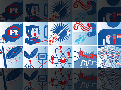 Top 10 Emerging Technologies of 2017
The World Economic Forum’s Expert Network and Global Future Councils in collaboration with Scientific American and its Board of Advisors announced the top 10 emerging technologies of 2017 on June 26 in Dalian, China where the 2017 Summer Davos Forum is being held. Each technology was chosen for its potential to improve lives, transform industries, and safeguard the planet.
The KAIST delegation, headed by President Sung-Chul Shin, is participating in the forum’s diverse activities including IdeasLab and GULF (Global University Leaders Forum). KAIST is the only Korean representative participating in the IdeasLab. KAIST Distinguished Professor Sang Yup Lee of the Department of Chemical and Biomolecular Engineering, director of KAIST Institute, has served as a committee member of the Global Agenda Council on Emerging Technologies since 2012 and Global Future Council on the Fourth Industrial Revolution. He also chairs the Global Future Council on Biotechnologies.
Professor Lee said, “Very diverse technological breakthroughs were proposed for the final list of candidates. We made the final selections through very in-depth discussion with experts in each field.
We focused on the technologies which have a level of maturity that will enable them to be adopted widely within three to five years."
The top 10 emerging technologies are
(courtesy from https://
www.weforum.org/agenda/2017/06/these-are-the-top-10-emerging-technologies-of-2017):
2017 10대 기술.
1. Liquid biopsies
Liquid biopsies mark a step forward in the fight against cancer. First, they are an alternative where traditional tissue-based biopsies are not possible. Second, they provide a full spectrum of information compared to tissue samples, which only reflect the information available in the sample. Lastly, by homing in on circulating-tumor DNA (ctDNA), genetic material that routinely finds its way from cancer cells into the bloodstream, disease progression or resistance to treatment can be spotted much faster than otherwise relying on symptoms or imaging.
2. Harvesting clean water from air
The ability to extract clean water from air is not new, however existing techniques require high moisture levels and a lot of electricity. This is changing. A team from MIT and University of California, Berkeley has successfully tested a process using porous crystals that convert the water using no energy at all.
3. Deep learning for visual tasks
Computers are beginning to recognize images better than humans. Thanks to deep learning, an emerging field of artificial intelligence, computer-vision technologies are increasingly being used in applications as diverse as driving autonomous vehicles, medical diagnostics, damage assessment for insurance claims, and monitoring water levels and crop yield.
4. Liquid fuels from sunshine
Can we mimic the humble leaf to create artificial photosynthesis to generate and store energy? The prospects are looking increasingly positive. The answer lies in using sunlight-activated catalysts to split water molecules into water and hydrogen, and then using the same hydrogen to convert CO2 into hydrocarbons.
5. The Human Cell Atlas
An international collaboration aimed at deciphering the human body, called the Human Cell Atlas, was launched in October 2016. The project aims to identify every cell type in every tissue; learn exactly which genes, proteins, and other molecules are active in each type, and the processes which control that activity.
6. Precision farming
The Fourth Industrial Revolution is providing farmers with a new set of tools to boost crop yield and quality while reducing water and chemical use. Sensors, robots, GPS, mapping tools, and data-analytics software are all being used to customize the care that plants need.
7. Affordable catalysts for green vehicles
Progress is being made on a promising zero-emission technology, the hydrogen-fed fuel cell. Progress to date has been stymied by the high price of catalysts which contain platinum. However, much progress has been made in reducing reliance on this rare and expensive metal, and the latest developments involve catalysts that include no platinum, or in some cases no metal at all.
8. Genomic vaccines
Vaccines based on genes are superior to more conventional ones in a number of ways. They are faster to manufacture, which is crucial during violent outbreaks. Compared to manufacturing proteins in cell cultures or eggs, producing genetic material should also be simpler and less expensive.
9. Sustainable design of communities
Applying green construction to multiple buildings at once has the potential to revolutionize the amount of energy and water we consume. Sending locally-generated solar power to a smart microgrid could reduce electricity consumption by half and reduce carbon emissions to zero if a project currently under development at the University of California at Berkeley goes according to plan.
10. Quantum computing
Quantum computers’ almost limitless potential has only ever been matched by the difficulty and cost of their construction. This explains why today the small ones that have been built have not yet managed to exceed the power of supercomputers. But progress is being made and in 2016 the technology firm IBM provided public access to the first quantum computer in the cloud.
2017.06.28 View 13985
Top 10 Emerging Technologies of 2017
The World Economic Forum’s Expert Network and Global Future Councils in collaboration with Scientific American and its Board of Advisors announced the top 10 emerging technologies of 2017 on June 26 in Dalian, China where the 2017 Summer Davos Forum is being held. Each technology was chosen for its potential to improve lives, transform industries, and safeguard the planet.
The KAIST delegation, headed by President Sung-Chul Shin, is participating in the forum’s diverse activities including IdeasLab and GULF (Global University Leaders Forum). KAIST is the only Korean representative participating in the IdeasLab. KAIST Distinguished Professor Sang Yup Lee of the Department of Chemical and Biomolecular Engineering, director of KAIST Institute, has served as a committee member of the Global Agenda Council on Emerging Technologies since 2012 and Global Future Council on the Fourth Industrial Revolution. He also chairs the Global Future Council on Biotechnologies.
Professor Lee said, “Very diverse technological breakthroughs were proposed for the final list of candidates. We made the final selections through very in-depth discussion with experts in each field.
We focused on the technologies which have a level of maturity that will enable them to be adopted widely within three to five years."
The top 10 emerging technologies are
(courtesy from https://
www.weforum.org/agenda/2017/06/these-are-the-top-10-emerging-technologies-of-2017):
2017 10대 기술.
1. Liquid biopsies
Liquid biopsies mark a step forward in the fight against cancer. First, they are an alternative where traditional tissue-based biopsies are not possible. Second, they provide a full spectrum of information compared to tissue samples, which only reflect the information available in the sample. Lastly, by homing in on circulating-tumor DNA (ctDNA), genetic material that routinely finds its way from cancer cells into the bloodstream, disease progression or resistance to treatment can be spotted much faster than otherwise relying on symptoms or imaging.
2. Harvesting clean water from air
The ability to extract clean water from air is not new, however existing techniques require high moisture levels and a lot of electricity. This is changing. A team from MIT and University of California, Berkeley has successfully tested a process using porous crystals that convert the water using no energy at all.
3. Deep learning for visual tasks
Computers are beginning to recognize images better than humans. Thanks to deep learning, an emerging field of artificial intelligence, computer-vision technologies are increasingly being used in applications as diverse as driving autonomous vehicles, medical diagnostics, damage assessment for insurance claims, and monitoring water levels and crop yield.
4. Liquid fuels from sunshine
Can we mimic the humble leaf to create artificial photosynthesis to generate and store energy? The prospects are looking increasingly positive. The answer lies in using sunlight-activated catalysts to split water molecules into water and hydrogen, and then using the same hydrogen to convert CO2 into hydrocarbons.
5. The Human Cell Atlas
An international collaboration aimed at deciphering the human body, called the Human Cell Atlas, was launched in October 2016. The project aims to identify every cell type in every tissue; learn exactly which genes, proteins, and other molecules are active in each type, and the processes which control that activity.
6. Precision farming
The Fourth Industrial Revolution is providing farmers with a new set of tools to boost crop yield and quality while reducing water and chemical use. Sensors, robots, GPS, mapping tools, and data-analytics software are all being used to customize the care that plants need.
7. Affordable catalysts for green vehicles
Progress is being made on a promising zero-emission technology, the hydrogen-fed fuel cell. Progress to date has been stymied by the high price of catalysts which contain platinum. However, much progress has been made in reducing reliance on this rare and expensive metal, and the latest developments involve catalysts that include no platinum, or in some cases no metal at all.
8. Genomic vaccines
Vaccines based on genes are superior to more conventional ones in a number of ways. They are faster to manufacture, which is crucial during violent outbreaks. Compared to manufacturing proteins in cell cultures or eggs, producing genetic material should also be simpler and less expensive.
9. Sustainable design of communities
Applying green construction to multiple buildings at once has the potential to revolutionize the amount of energy and water we consume. Sending locally-generated solar power to a smart microgrid could reduce electricity consumption by half and reduce carbon emissions to zero if a project currently under development at the University of California at Berkeley goes according to plan.
10. Quantum computing
Quantum computers’ almost limitless potential has only ever been matched by the difficulty and cost of their construction. This explains why today the small ones that have been built have not yet managed to exceed the power of supercomputers. But progress is being made and in 2016 the technology firm IBM provided public access to the first quantum computer in the cloud.
2017.06.28 View 13985 -
 The Embassy Day Builds the Global Presence of KAIST
(Photo caption: Diplomats and KAIST faculty pose at the Embassy Day KAIST hosted on June 23.)
KAIST is stepping up its initiative for building global competitiveness. The Embassy Day hosted on June 23 will be a stepping stone to diversify its channels for promoting the global presence of KAIST. KAIST invited the foreign diplomatic corps from Seoul to share their successful journey to emerge as the world-class university. The event featured KAIST’s research highlights, academic experiences, and global environment through presentations by faculty and students.
KAIST President Sung-Chul Shin said in his welcoming speech that he hopes for brains from around the world to come to KAIST and believes this event will serve as an opportunity to spread the global reputation of KAIST more widely. President Shin, who took office in March, ambitiously hosted this event for the first time, saying, “We didn’t expect this big of a response from the diplomats. The presence of this leading group of diplomats reflects how KAIST’s reputation has blossomed.”
Nearly 100 diplomats from 65 countries attended the event held at the Grand Hyatt Seoul. Among the participants were ambassadors from 33 countries including Australian Amb. James Choi, Canadian Amb. Eric Walsh, and German Amb. Stephan Auer, reflecting the growing interest in the advancements in science and technology education and innovation in KAIST.
The entire leadership team of KAIST turned out for the event including Provost O-Ok Park, Associate Vice President of the International Office Jay Hyung Lee, and Dean of Admissions Hayong Shin to provide an update on KAIST activities as well as admission policies, and make a new network with the foreign envoys.
At the event, KAIST presented some of its latest research highlights that are gaining international acclaim. Professor Jun-ho Oh, director at the Humanoid Robot Research Center talked on the short history of the development of the KAIST humanoid robot, HUBO, which won the DARPA Robotics Challenge (DRC) in 2015. Distinguished Professor Sang-Yup Lee, dean of the KAIST Institute, which is the center of multidisciplinary research projects in KAIST, made a presentation on advances in metabolic engineering. In addition, Professor David Helfman of the Department of Biological Science shared his research on breast cancer and metastasis.
Foreign students and faculty shared their experiences on becoming part of the KAIST community during the testimonial session. In particular, the story of Professor Jean-Charles Bazin of the Graduate School of Culture Technology was quite moving. Originally from France, Professor Bazin talked about his unique career path, starting as an exchange student at KAIST before settling down as a faculty member here. He cited the high caliber group of faculty as one of the reasons he completed his Ph.D. at KAIST. “Most of the faculty members are from top institutions in the US, Europe, and around the world, so they have very resourceful contacts with distinguished researchers and scholars abroad. That helped me make up my mind to choose KAIST,” he said.
Currently, 179 foreign faculty and researchers from over 31 countries, representing 8.7% of the total faculty, are working at KAIST. Also, 710 foreign students from 86 countries, representing about 8% of the total students, are now studying at KAIST.
President Shin continued, “In this complex global era, brains follow the best path to where they can reach their potential. KAIST is now gaining tremendous strength by becoming a magnet for talents from around the world. We would like to recruit these brains to create new knowledge with a global impact. Then we will become true global university with supremacy in research and education.
President Shin said KAIST is gearing up for another round of innovation initiatives in education, convergence research, technology commercialization, future strategies, and globalization. He emphasized that globalization of the campus is a must for building up our global competitiveness.
(Photo caption from the top: President Shin greets participant. Professor Oh explains the functions of the HUBO. Professor Helfman presents on his research of breast cancer and metastasis. KAIST a capella group showcases singing skills at the event. Participants meet and greet at the Embassy Day.)
2017.06.23 View 11013
The Embassy Day Builds the Global Presence of KAIST
(Photo caption: Diplomats and KAIST faculty pose at the Embassy Day KAIST hosted on June 23.)
KAIST is stepping up its initiative for building global competitiveness. The Embassy Day hosted on June 23 will be a stepping stone to diversify its channels for promoting the global presence of KAIST. KAIST invited the foreign diplomatic corps from Seoul to share their successful journey to emerge as the world-class university. The event featured KAIST’s research highlights, academic experiences, and global environment through presentations by faculty and students.
KAIST President Sung-Chul Shin said in his welcoming speech that he hopes for brains from around the world to come to KAIST and believes this event will serve as an opportunity to spread the global reputation of KAIST more widely. President Shin, who took office in March, ambitiously hosted this event for the first time, saying, “We didn’t expect this big of a response from the diplomats. The presence of this leading group of diplomats reflects how KAIST’s reputation has blossomed.”
Nearly 100 diplomats from 65 countries attended the event held at the Grand Hyatt Seoul. Among the participants were ambassadors from 33 countries including Australian Amb. James Choi, Canadian Amb. Eric Walsh, and German Amb. Stephan Auer, reflecting the growing interest in the advancements in science and technology education and innovation in KAIST.
The entire leadership team of KAIST turned out for the event including Provost O-Ok Park, Associate Vice President of the International Office Jay Hyung Lee, and Dean of Admissions Hayong Shin to provide an update on KAIST activities as well as admission policies, and make a new network with the foreign envoys.
At the event, KAIST presented some of its latest research highlights that are gaining international acclaim. Professor Jun-ho Oh, director at the Humanoid Robot Research Center talked on the short history of the development of the KAIST humanoid robot, HUBO, which won the DARPA Robotics Challenge (DRC) in 2015. Distinguished Professor Sang-Yup Lee, dean of the KAIST Institute, which is the center of multidisciplinary research projects in KAIST, made a presentation on advances in metabolic engineering. In addition, Professor David Helfman of the Department of Biological Science shared his research on breast cancer and metastasis.
Foreign students and faculty shared their experiences on becoming part of the KAIST community during the testimonial session. In particular, the story of Professor Jean-Charles Bazin of the Graduate School of Culture Technology was quite moving. Originally from France, Professor Bazin talked about his unique career path, starting as an exchange student at KAIST before settling down as a faculty member here. He cited the high caliber group of faculty as one of the reasons he completed his Ph.D. at KAIST. “Most of the faculty members are from top institutions in the US, Europe, and around the world, so they have very resourceful contacts with distinguished researchers and scholars abroad. That helped me make up my mind to choose KAIST,” he said.
Currently, 179 foreign faculty and researchers from over 31 countries, representing 8.7% of the total faculty, are working at KAIST. Also, 710 foreign students from 86 countries, representing about 8% of the total students, are now studying at KAIST.
President Shin continued, “In this complex global era, brains follow the best path to where they can reach their potential. KAIST is now gaining tremendous strength by becoming a magnet for talents from around the world. We would like to recruit these brains to create new knowledge with a global impact. Then we will become true global university with supremacy in research and education.
President Shin said KAIST is gearing up for another round of innovation initiatives in education, convergence research, technology commercialization, future strategies, and globalization. He emphasized that globalization of the campus is a must for building up our global competitiveness.
(Photo caption from the top: President Shin greets participant. Professor Oh explains the functions of the HUBO. Professor Helfman presents on his research of breast cancer and metastasis. KAIST a capella group showcases singing skills at the event. Participants meet and greet at the Embassy Day.)
2017.06.23 View 11013 -
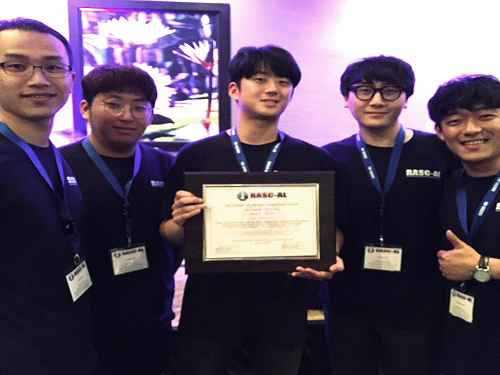 Winning Best in Theme Award in NASA RASC-AL
A students team from the Department of Aerospace Engineering won the Best in Theme Award for moon exploration system design at Revolutionary Aerospace Systems Concepts - Academic Linkage (RASC-AL), an aerospace mission system design competition organized by NASA in the USA.
The KAIST team, consisting of Jaeyoul Ko, Jongeun Suh, Juseong Lee, Sukmin Choi, and Eunkwang Lee, and supervised by Professor Jaemyung Ahn, competed as a joint team with Texas Tech University and the Royal Melbourne Institute of Technology in Australia,
The joint team was selected as one of the 14 finalists after two preliminary rounds. The finals of RASC-AL Forum took place from May 30 to June 3 in Florida. The team received the top prize with their design entitled ‘Earth to Lunar Interchangeable Transportation Environment (ELITE) for Logistics Delivery Systems’, one of the four themes of the competition.
Since 2002, RASC-AL competitions, managed by NASA, have been held with themes on innovative aerospace system and missions, in which world-class undergraduate and graduate students have participated.
This year’s themes were ▲ Lightweight Exercise Suite ▲ Airlock Design ▲ Commercially Enabled LEO/Mars Habitable Module and ▲ Logistics Delivery System.
Moon exploration requires a great deal of time and supplies. The KAIST team has been researching supply delivery systems in space for long-term manned moon exploration with their joint team for the last eight months. In particular, incidents can occur during the initial stages of long-term manned moon exploration missions that are unpredictable during system design and planning. Therefore, to cope with such unpredictability in the mission, the KAIST team deduced a system and an operational concept with increased flexibility to maximize the cost effectiveness of the supply transport.
The spacecraft was divided into propulsion and transport modules based on their functionalities, and can allow the flexibility by switching the transport module according to the demands of the moon base. The operational flexibility and cost effectiveness are further increased by introducing multiple departure orbits from the Earth (e.g. low Earth orbit vs. geosynchronous Earth orbit) enabled by utilization of various launch vehicles.
Professor Ahn, the advisor for the team, said, “I am proud of the students who collaborated with the international joint teams and achieved great result.” He continued, “I believe this to be the result of continuous efforts and initiatives of the department for system design-centered education. We will keep providing high-quality system design and education through various opportunities such as international cooperation in design education.”
(Photo caption: KAIST team of the Department of Aerospace Engineering poses after winning the Best in Theme Award in NASA's RASC-AL)
2017.06.22 View 10252
Winning Best in Theme Award in NASA RASC-AL
A students team from the Department of Aerospace Engineering won the Best in Theme Award for moon exploration system design at Revolutionary Aerospace Systems Concepts - Academic Linkage (RASC-AL), an aerospace mission system design competition organized by NASA in the USA.
The KAIST team, consisting of Jaeyoul Ko, Jongeun Suh, Juseong Lee, Sukmin Choi, and Eunkwang Lee, and supervised by Professor Jaemyung Ahn, competed as a joint team with Texas Tech University and the Royal Melbourne Institute of Technology in Australia,
The joint team was selected as one of the 14 finalists after two preliminary rounds. The finals of RASC-AL Forum took place from May 30 to June 3 in Florida. The team received the top prize with their design entitled ‘Earth to Lunar Interchangeable Transportation Environment (ELITE) for Logistics Delivery Systems’, one of the four themes of the competition.
Since 2002, RASC-AL competitions, managed by NASA, have been held with themes on innovative aerospace system and missions, in which world-class undergraduate and graduate students have participated.
This year’s themes were ▲ Lightweight Exercise Suite ▲ Airlock Design ▲ Commercially Enabled LEO/Mars Habitable Module and ▲ Logistics Delivery System.
Moon exploration requires a great deal of time and supplies. The KAIST team has been researching supply delivery systems in space for long-term manned moon exploration with their joint team for the last eight months. In particular, incidents can occur during the initial stages of long-term manned moon exploration missions that are unpredictable during system design and planning. Therefore, to cope with such unpredictability in the mission, the KAIST team deduced a system and an operational concept with increased flexibility to maximize the cost effectiveness of the supply transport.
The spacecraft was divided into propulsion and transport modules based on their functionalities, and can allow the flexibility by switching the transport module according to the demands of the moon base. The operational flexibility and cost effectiveness are further increased by introducing multiple departure orbits from the Earth (e.g. low Earth orbit vs. geosynchronous Earth orbit) enabled by utilization of various launch vehicles.
Professor Ahn, the advisor for the team, said, “I am proud of the students who collaborated with the international joint teams and achieved great result.” He continued, “I believe this to be the result of continuous efforts and initiatives of the department for system design-centered education. We will keep providing high-quality system design and education through various opportunities such as international cooperation in design education.”
(Photo caption: KAIST team of the Department of Aerospace Engineering poses after winning the Best in Theme Award in NASA's RASC-AL)
2017.06.22 View 10252 -
 KAIST to Participate in the Summer Davos Forum
KAIST will participate in the 2017 Summer Davos Forum in Dalian, China from June 27 to 29. The Summer Davos Forum with the official title “Annual Meeting of New Champions” is an annual international meeting co-hosted by China and the World Economic Forum (WEF) to address global issues which has been held since 2007.
Focusing on this year’s theme ‘Achieving Inclusive Growth in the Fourth Industrial Revolution,’ science and technology experts from 90 different countries will participate in various sessions to present on and discuss pending global innovative issues. KAIST is to be the only Korean university to run ‘IdeasLab,’ in which researchers will introduce current research trends and discuss ideas with global leaders. This is the sixth year for KAIST to run IdeasLab.
This year’s IdeasLab has the theme ‘Materials of the Future,’ and will include presentations and discussions on materials developed at KAIST which could lead the Fourth Industrial Revolution. President Sung-Chul Shin, the chairman of the session, will first introduce the current status of KAIST and IdeasLab, followed by a presentation of cutting-edge integrated research findings by KAIST professors.
President Shin will also participate in various sessions organized by the Global University Leaders Forum (GULF) as discussion leader. President Shin is the only Korean member of GULF, a community comprised of the presidents of the world’s top 27 universities. Other members include the presidents of the University of Oxford and the University of Cambridge in the U.K., MIT, Harvard, Stanford, and Columbia Universities in the US, and the University of Tokyo in Japan.
Further, President Shin will participate in a strategy session for inclusive growth in the era of the Fourth Industrial Revolution and a meeting with the WEF directors.
The Dean of KAIST Institutes, Distinguished Professor Sang Yup Lee from the Chemical and Biomolecular Engineering Department, who has been invited to the Davos Forum and Summer Davos Forum for the last 15 years, is to present in the ‘Future of Life: Medicine’ session to introduce advancements in traditional medicine through systems biology such as his research on microbiomes (gut microbes).
Professor Lee, as the chair of the Global Future Council on Biotechnology at the WEF, and committee member of the Annual Meeting of the Global Future Councils on the Fourth Industrial Revolution, is to participate in various bio-sessions and the Fourth Industrial Revolution banquet session to lead the discussions.
President Shin said, “KAIST has been sharing global research findings with global leaders through IdeasLab at the Davos Forum for the past six years and it has always been well received.” He continued, “The forum will be the place for in-depth discussion on the technological changes that accompany the Fourth Industrial Revolution and human-centered development plan, as well as introducing innovative research and integrated research findings from KAIST.”
This year’s speakers include Li Keqiang, the current Premier of the State Council of China; Guo Ping, the rotating C.E.O. of Huawei; and Ya-Qin Zhang, the President of Baidu, a company leading technological innovation in various fields such as robotics and autonomous vehicles. Two thousand distinguished guests in politics, administration, finance, and academia from 90 countries are to participate in the meeting.
2017.06.21 View 10106
KAIST to Participate in the Summer Davos Forum
KAIST will participate in the 2017 Summer Davos Forum in Dalian, China from June 27 to 29. The Summer Davos Forum with the official title “Annual Meeting of New Champions” is an annual international meeting co-hosted by China and the World Economic Forum (WEF) to address global issues which has been held since 2007.
Focusing on this year’s theme ‘Achieving Inclusive Growth in the Fourth Industrial Revolution,’ science and technology experts from 90 different countries will participate in various sessions to present on and discuss pending global innovative issues. KAIST is to be the only Korean university to run ‘IdeasLab,’ in which researchers will introduce current research trends and discuss ideas with global leaders. This is the sixth year for KAIST to run IdeasLab.
This year’s IdeasLab has the theme ‘Materials of the Future,’ and will include presentations and discussions on materials developed at KAIST which could lead the Fourth Industrial Revolution. President Sung-Chul Shin, the chairman of the session, will first introduce the current status of KAIST and IdeasLab, followed by a presentation of cutting-edge integrated research findings by KAIST professors.
President Shin will also participate in various sessions organized by the Global University Leaders Forum (GULF) as discussion leader. President Shin is the only Korean member of GULF, a community comprised of the presidents of the world’s top 27 universities. Other members include the presidents of the University of Oxford and the University of Cambridge in the U.K., MIT, Harvard, Stanford, and Columbia Universities in the US, and the University of Tokyo in Japan.
Further, President Shin will participate in a strategy session for inclusive growth in the era of the Fourth Industrial Revolution and a meeting with the WEF directors.
The Dean of KAIST Institutes, Distinguished Professor Sang Yup Lee from the Chemical and Biomolecular Engineering Department, who has been invited to the Davos Forum and Summer Davos Forum for the last 15 years, is to present in the ‘Future of Life: Medicine’ session to introduce advancements in traditional medicine through systems biology such as his research on microbiomes (gut microbes).
Professor Lee, as the chair of the Global Future Council on Biotechnology at the WEF, and committee member of the Annual Meeting of the Global Future Councils on the Fourth Industrial Revolution, is to participate in various bio-sessions and the Fourth Industrial Revolution banquet session to lead the discussions.
President Shin said, “KAIST has been sharing global research findings with global leaders through IdeasLab at the Davos Forum for the past six years and it has always been well received.” He continued, “The forum will be the place for in-depth discussion on the technological changes that accompany the Fourth Industrial Revolution and human-centered development plan, as well as introducing innovative research and integrated research findings from KAIST.”
This year’s speakers include Li Keqiang, the current Premier of the State Council of China; Guo Ping, the rotating C.E.O. of Huawei; and Ya-Qin Zhang, the President of Baidu, a company leading technological innovation in various fields such as robotics and autonomous vehicles. Two thousand distinguished guests in politics, administration, finance, and academia from 90 countries are to participate in the meeting.
2017.06.21 View 10106 -
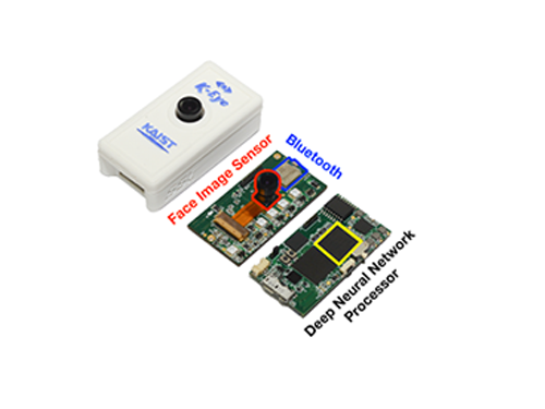 Face Recognition System 'K-Eye' Presented by KAIST
Artificial intelligence (AI) is one of the key emerging technologies. Global IT companies are competitively launching the newest technologies and competition is heating up more than ever. However, most AI technologies focus on software and their operating speeds are low, making them a poor fit for mobile devices. Therefore, many big companies are investing to develop semiconductor chips for running AI programs with low power requirements but at high speeds.
A research team led by Professor Hoi-Jun Yoo of the Department of Electrical Engineering has developed a semiconductor chip, CNNP (CNN Processor), that runs AI algorithms with ultra-low power, and K-Eye, a face recognition system using CNNP. The system was made in collaboration with a start-up company, UX Factory Co.
The K-Eye series consists of two types: a wearable type and a dongle type. The wearable type device can be used with a smartphone via Bluetooth, and it can operate for more than 24 hours with its internal battery. Users hanging K-Eye around their necks can conveniently check information about people by using their smartphone or smart watch, which connects K-Eye and allows users to access a database via their smart devices. A smartphone with K-EyeQ, the dongle type device, can recognize and share information about users at any time.
When recognizing that an authorized user is looking at its screen, the smartphone automatically turns on without a passcode, fingerprint, or iris authentication. Since it can distinguish whether an input face is coming from a saved photograph versus a real person, the smartphone cannot be tricked by the user’s photograph.
The K-Eye series carries other distinct features. It can detect a face at first and then recognize it, and it is possible to maintain “Always-on” status with low power consumption of less than 1mW. To accomplish this, the research team proposed two key technologies: an image sensor with “Always-on” face detection and the CNNP face recognition chip.
The first key technology, the “Always-on” image sensor, can determine if there is a face in its camera range. Then, it can capture frames and set the device to operate only when a face exists, reducing the standby power significantly. The face detection sensor combines analog and digital processing to reduce power consumption. With this approach, the analog processor, combined with the CMOS Image Sensor array, distinguishes the background area from the area likely to include a face, and the digital processor then detects the face only in the selected area. Hence, it becomes effective in terms of frame capture, face detection processing, and memory usage.
The second key technology, CNNP, achieved incredibly low power consumption by optimizing a convolutional neural network (CNN) in the areas of circuitry, architecture, and algorithms. First, the on-chip memory integrated in CNNP is specially designed to enable data to be read in a vertical direction as well as in a horizontal direction. Second, it has immense computational power with 1024 multipliers and accumulators operating in parallel and is capable of directly transferring the temporal results to each other without accessing to the external memory or on-chip communication network. Third, convolution calculations with a two-dimensional filter in the CNN algorithm are approximated into two sequential calculations of one-dimensional filters to achieve higher speeds and lower power consumption.
With these new technologies, CNNP achieved 97% high accuracy but consumed only 1/5000 power of the GPU. Face recognition can be performed with only 0.62mW of power consumption, and the chip can show higher performance than the GPU by using more power.
These chips were developed by Kyeongryeol Bong, a Ph. D. student under Professor Yoo and presented at the International Solid-State Circuit Conference (ISSCC) held in San Francisco in February. CNNP, which has the lowest reported power consumption in the world, has achieved a great deal of attention and has led to the development of the present K-Eye series for face recognition.
Professor Yoo said “AI - processors will lead the era of the Fourth Industrial Revolution. With the development of this AI chip, we expect Korea to take the lead in global AI technology.”
The research team and UX Factory Co. are preparing to commercialize the K-Eye series by the end of this year. According to a market researcher IDC, the market scale of the AI industry will grow from $127 billion last year to $165 billion in this year.
(Photo caption: Schematic diagram of K-Eye system)
2017.06.14 View 17600
Face Recognition System 'K-Eye' Presented by KAIST
Artificial intelligence (AI) is one of the key emerging technologies. Global IT companies are competitively launching the newest technologies and competition is heating up more than ever. However, most AI technologies focus on software and their operating speeds are low, making them a poor fit for mobile devices. Therefore, many big companies are investing to develop semiconductor chips for running AI programs with low power requirements but at high speeds.
A research team led by Professor Hoi-Jun Yoo of the Department of Electrical Engineering has developed a semiconductor chip, CNNP (CNN Processor), that runs AI algorithms with ultra-low power, and K-Eye, a face recognition system using CNNP. The system was made in collaboration with a start-up company, UX Factory Co.
The K-Eye series consists of two types: a wearable type and a dongle type. The wearable type device can be used with a smartphone via Bluetooth, and it can operate for more than 24 hours with its internal battery. Users hanging K-Eye around their necks can conveniently check information about people by using their smartphone or smart watch, which connects K-Eye and allows users to access a database via their smart devices. A smartphone with K-EyeQ, the dongle type device, can recognize and share information about users at any time.
When recognizing that an authorized user is looking at its screen, the smartphone automatically turns on without a passcode, fingerprint, or iris authentication. Since it can distinguish whether an input face is coming from a saved photograph versus a real person, the smartphone cannot be tricked by the user’s photograph.
The K-Eye series carries other distinct features. It can detect a face at first and then recognize it, and it is possible to maintain “Always-on” status with low power consumption of less than 1mW. To accomplish this, the research team proposed two key technologies: an image sensor with “Always-on” face detection and the CNNP face recognition chip.
The first key technology, the “Always-on” image sensor, can determine if there is a face in its camera range. Then, it can capture frames and set the device to operate only when a face exists, reducing the standby power significantly. The face detection sensor combines analog and digital processing to reduce power consumption. With this approach, the analog processor, combined with the CMOS Image Sensor array, distinguishes the background area from the area likely to include a face, and the digital processor then detects the face only in the selected area. Hence, it becomes effective in terms of frame capture, face detection processing, and memory usage.
The second key technology, CNNP, achieved incredibly low power consumption by optimizing a convolutional neural network (CNN) in the areas of circuitry, architecture, and algorithms. First, the on-chip memory integrated in CNNP is specially designed to enable data to be read in a vertical direction as well as in a horizontal direction. Second, it has immense computational power with 1024 multipliers and accumulators operating in parallel and is capable of directly transferring the temporal results to each other without accessing to the external memory or on-chip communication network. Third, convolution calculations with a two-dimensional filter in the CNN algorithm are approximated into two sequential calculations of one-dimensional filters to achieve higher speeds and lower power consumption.
With these new technologies, CNNP achieved 97% high accuracy but consumed only 1/5000 power of the GPU. Face recognition can be performed with only 0.62mW of power consumption, and the chip can show higher performance than the GPU by using more power.
These chips were developed by Kyeongryeol Bong, a Ph. D. student under Professor Yoo and presented at the International Solid-State Circuit Conference (ISSCC) held in San Francisco in February. CNNP, which has the lowest reported power consumption in the world, has achieved a great deal of attention and has led to the development of the present K-Eye series for face recognition.
Professor Yoo said “AI - processors will lead the era of the Fourth Industrial Revolution. With the development of this AI chip, we expect Korea to take the lead in global AI technology.”
The research team and UX Factory Co. are preparing to commercialize the K-Eye series by the end of this year. According to a market researcher IDC, the market scale of the AI industry will grow from $127 billion last year to $165 billion in this year.
(Photo caption: Schematic diagram of K-Eye system)
2017.06.14 View 17600 -
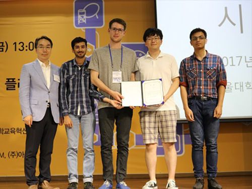
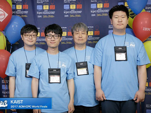 KAIST Team Wins Bronze Medal at Int'l Programming Contest
A KAIST Team consisting of undergraduate students from the School of Computing and Department of Mathematical Science received a bronze medal and First Problem Solver award at an international undergraduate programming competition, The Association for Computing Machinery-International Collegiate Programming Contest (ACM-ICPC) World Finals.
The 41st ACM-ICPC hosted by ACM and funded by IBM was held in South Dakota in the US on May 25. The competition, first held in 1977, is aimed at undergraduate students from around the world. A total of 50,000 students from 2900 universities and 103 countries participated in the regional competition and 400 students competed in the finals.
The competition required teams of three to solve 12 problems. The KAIST team was coached by Emeritus Professor Sung-Yong Shin and Professor Taisook Han. The student contestants were Jihoon Ko and Hanpil Kang from the School of Computing and Jongwoon Lee from the Department of Mathematical Science. The team finished ranked 9th, receiving a bronze medal and a $3000 prize. Additionally, the team was the first to solve all the problems and received the First Problem Solver award. Detailed score information can be found on. https://icpc.baylor.edu/scoreboard/
(Photo caption: Professor Taisook Han and his students)
2017.06.12 View 11402
KAIST Team Wins Bronze Medal at Int'l Programming Contest
A KAIST Team consisting of undergraduate students from the School of Computing and Department of Mathematical Science received a bronze medal and First Problem Solver award at an international undergraduate programming competition, The Association for Computing Machinery-International Collegiate Programming Contest (ACM-ICPC) World Finals.
The 41st ACM-ICPC hosted by ACM and funded by IBM was held in South Dakota in the US on May 25. The competition, first held in 1977, is aimed at undergraduate students from around the world. A total of 50,000 students from 2900 universities and 103 countries participated in the regional competition and 400 students competed in the finals.
The competition required teams of three to solve 12 problems. The KAIST team was coached by Emeritus Professor Sung-Yong Shin and Professor Taisook Han. The student contestants were Jihoon Ko and Hanpil Kang from the School of Computing and Jongwoon Lee from the Department of Mathematical Science. The team finished ranked 9th, receiving a bronze medal and a $3000 prize. Additionally, the team was the first to solve all the problems and received the First Problem Solver award. Detailed score information can be found on. https://icpc.baylor.edu/scoreboard/
(Photo caption: Professor Taisook Han and his students)
2017.06.12 View 11402 -
 KATT Tops at Appropriate Technology Competition
The KAIST Appropriate Technology Team (KATT) consisting of KAIST international students received gold and bronze awards at ‘the 9th Creative Design Competition for the Other 90%’. This year’s competition was hosted by the Ministry of Science, ICT and Future Planning at Seoul National University’s Global Convention Plaza on May 26. Undergraduate and graduate students nationwide formed 65 teams to participate in the competition.
The aim of the competition is to discover appropriate technology and sustainable design items to enhance quality of life for those with no or little access to science technology and its products around the world. This year’s competition categorized the designs into IT; water and energy; agriculture, hygiene, safety, and housing; and education. The teams were evaluated on their presentations and prototypes.
KATT produced alarm warning bracelets for people in developing countries and smart hybrid dryers for agricultural products. The alarm warning bracelets were designed for those living in tsunami risk zones; they use wireless communication technology to receive and transmit warning signals and can be produced for less than $4.
The smart hybrid dryers featured solar energy generation, aimed to help those with low income in subtropical, low-altitude regions with unstable climates, since there are currently no drying methods for agricultural products without direct exposure to sunlight. Therefore, the hybrid dryers allowed drying regardless of the weather, and thus increased the storage and distribution efficiency of agricultural products.
Ashar Alam from India who participated in developing the alarm warning bracelet said, “Through the appropriate technology club, I recognized problems in India that also affect neighboring countries such as Indonesia and Bangladesh. I wanted to actively use the science and technology knowledge I have accumulated in KAIST for the less fortunate.” He continued, “It was meaningful to develop the product using the respective talents of students from various countries with the spirit of developing appropriate technology.”
(Photo caption: Alarm warning bracelet team received the gold award)
2017.06.12 View 9010
KATT Tops at Appropriate Technology Competition
The KAIST Appropriate Technology Team (KATT) consisting of KAIST international students received gold and bronze awards at ‘the 9th Creative Design Competition for the Other 90%’. This year’s competition was hosted by the Ministry of Science, ICT and Future Planning at Seoul National University’s Global Convention Plaza on May 26. Undergraduate and graduate students nationwide formed 65 teams to participate in the competition.
The aim of the competition is to discover appropriate technology and sustainable design items to enhance quality of life for those with no or little access to science technology and its products around the world. This year’s competition categorized the designs into IT; water and energy; agriculture, hygiene, safety, and housing; and education. The teams were evaluated on their presentations and prototypes.
KATT produced alarm warning bracelets for people in developing countries and smart hybrid dryers for agricultural products. The alarm warning bracelets were designed for those living in tsunami risk zones; they use wireless communication technology to receive and transmit warning signals and can be produced for less than $4.
The smart hybrid dryers featured solar energy generation, aimed to help those with low income in subtropical, low-altitude regions with unstable climates, since there are currently no drying methods for agricultural products without direct exposure to sunlight. Therefore, the hybrid dryers allowed drying regardless of the weather, and thus increased the storage and distribution efficiency of agricultural products.
Ashar Alam from India who participated in developing the alarm warning bracelet said, “Through the appropriate technology club, I recognized problems in India that also affect neighboring countries such as Indonesia and Bangladesh. I wanted to actively use the science and technology knowledge I have accumulated in KAIST for the less fortunate.” He continued, “It was meaningful to develop the product using the respective talents of students from various countries with the spirit of developing appropriate technology.”
(Photo caption: Alarm warning bracelet team received the gold award)
2017.06.12 View 9010 -
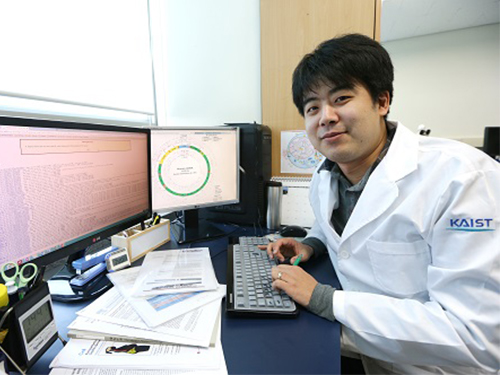 Mutations Unveiled that Predispose Lung Cancer Cells to Refractory Histologic Transformation
Cancer pedigree analysis reveals the mutations in RB1 and TP53 genes play a key role in treatment-resistant, cancer cell-type transformation during EGFR inhibitor therapy for lung cancers.
Research led by Korean medical scientists has discovered that a specific type of drug resistance mechanism to EGFR inhibitor therapy in lung cancer is predisposed by mutations in two canonical cancer-related genes: RB1 and TP53. Published in Journal of Clinical Oncology on May 12, the study also found those mutations can be detectable in patients' tumors at the point of clinical diagnosis. Therefore, it can be used as strong markers in clinic for predicting poor outcome for the targeted treatment for lung adenocarcinoma.
Lung adenocarcinoma is the most common type of lung cancer, and about 15% of patients in Western countries and 50% of patients in Asian countries have mutations in the EGFR gene, which is critical for the development of lung cancer. Patients with lung adenocarcinoma harboring the EGFR mutation show favorable responses to EGFR inhibitors such as erlotinib (Tarceva) or gefitinib (Iressa), but ultimately relapse with drug-resistant tumors. Since the initial report in 2006, it has been known that in about 5~15% of patients, the lung adenocarcinoma cells undergo a mysterious transformation into a very different cancer cell type called “small cell lung cancer,” a much more aggressive lung cancer subtype, common in cigarette smokers.
To find out the genetic basis of this process, the researchers compared the genome sequences of multiple cancer tissues acquired during the treatment courses of patients whose tumors underwent small-cell transformation. They reconstructed the cancer cell pedigree by comparing mutations between cancer tissues, and identified that RB1 and TP53 genes are completely inactivated by mutations already in their lung adenocarcinoma tissues.
"We tried to compare the somatic mutational profile of pre-EGFR inhibitor treatment lung adenocarcinomas and post-treatment small cell carcinomas and to reconstruct the pedigrees of the cancer evolution in each patient. Strikingly, both copies of RB1 and TP53 genes were already inactivated at the stage of lung adenocarcinomas in all sequenced cases," said Dr. Jake June-Koo Lee, the first author from KAIST.
They further pursued the clinical implications of RB1 and TP53 inactivation by investigating 75 EGFR-mutated lung adenocarcinoma tissues from patients who received EGFR inhibitor therapy, including patients with small-cell transformation. In this analysis, the lung adenocarcinomas with a complete inactivation of both RB1 and TP53 genes tended to have a 43-times greater risk of transformation into small cell lung cancer during their EGFR inhibitor treatment courses.
Dr. Young Seok Ju, the co-last author from KAIST, explained, "This study shows the power of entire genome analyses to better understand the mechanisms underlying mysterious phenomenon encountered in clinic. Upon accurate bioinformatics, we are finding cancer-specific somatic mutations from the whole-genomes of patients’ cancer cells. These mutations allow us to track the evolution of cancer cells throughout the extraordinary clinical course of a special set of lung cancers."
The complete inactivation of both RB1 and TP53 tumor suppressor genes is found in a minor (<10%) subset of lung adenocarcinoma. This study suggests that the clinical course against targeted therapy is endogenously different for the cancers in the subgroup, and specific drug-resistance mechanisms are predisposed by the two genetic mutations. Indeed, RB1 and TP53 double inactivation is a genetic hallmark of primary small cell lung cancer, observed in nearly all cases.
"We are actively investigating patient tumor tissues to develop optimal surveillance plans and treatment options for patients with lung adenocarcinomas more prone to small-cell transformation," said Dr. Tae Min Kim, the co-last author from Seoul National University Hospital.
The researchers are implementing their findings into lung cancer clinics by screening the RB1 and TP53 mutational status in lung adenocarcinoma patients receiving EGFR inhibitor treatment, and following their treatment courses to develop a treatment strategy for those patients.
This research (doi.org/10.1200/JCO.2016.71.9096) was funded by the National Research Foundation of Korea (NRF-2013H1A2A1032691 to J.-K.L., NRF-2014R1A2A2A05003665 to Y.T.K.); Korea Institute of Science and Technology Information (K-16-L03-C02-S02 to J.L.); and the Korea Health Technology R&D Project through the Korea Health Industry Development Institute, which was funded by the Ministry of Health and Welfare (HI14C1234 to T.M.K., HI16C2387 to Y.S.J.)
Figure. Phylogeny analysis of serially-acquired tumors
A. Phylogeny trees of sequenced cases (LC1−LC4) are reconstructed from the WGS data. Conceptual illustrations are depicted with grey color. Circles indicate major clones of the tumors. The length of each branch is proportional to the number of mutations that occurred in the branch. Mutations of cancer-related genes in each branch are indicated with arrows. The time points of relevant treatments are summarized below the trees.
B. Mutations of RB1 and TP53 in two early LADCs (LC1b and LC4a) are visualized using Integrative Genomics Viewer (left panel). Allele-specific copy number analysis shows loss of heterozygosity of chromosomes 13 and 17 in both early LADCs and EGFR TKI-resistant SCLCs (right panel).
C. Clonal evolution of LC1 is described with clinical history and tumor volumes. The horizontal axis represents the time from the diagnosis (0), and the vertical axis indicates the volume of tumors calculated from the computed tomography images.
Abbreviations: LADC, lung adenocarcinoma; SCLC, small cell lung cancer
2017.06.07 View 9461
Mutations Unveiled that Predispose Lung Cancer Cells to Refractory Histologic Transformation
Cancer pedigree analysis reveals the mutations in RB1 and TP53 genes play a key role in treatment-resistant, cancer cell-type transformation during EGFR inhibitor therapy for lung cancers.
Research led by Korean medical scientists has discovered that a specific type of drug resistance mechanism to EGFR inhibitor therapy in lung cancer is predisposed by mutations in two canonical cancer-related genes: RB1 and TP53. Published in Journal of Clinical Oncology on May 12, the study also found those mutations can be detectable in patients' tumors at the point of clinical diagnosis. Therefore, it can be used as strong markers in clinic for predicting poor outcome for the targeted treatment for lung adenocarcinoma.
Lung adenocarcinoma is the most common type of lung cancer, and about 15% of patients in Western countries and 50% of patients in Asian countries have mutations in the EGFR gene, which is critical for the development of lung cancer. Patients with lung adenocarcinoma harboring the EGFR mutation show favorable responses to EGFR inhibitors such as erlotinib (Tarceva) or gefitinib (Iressa), but ultimately relapse with drug-resistant tumors. Since the initial report in 2006, it has been known that in about 5~15% of patients, the lung adenocarcinoma cells undergo a mysterious transformation into a very different cancer cell type called “small cell lung cancer,” a much more aggressive lung cancer subtype, common in cigarette smokers.
To find out the genetic basis of this process, the researchers compared the genome sequences of multiple cancer tissues acquired during the treatment courses of patients whose tumors underwent small-cell transformation. They reconstructed the cancer cell pedigree by comparing mutations between cancer tissues, and identified that RB1 and TP53 genes are completely inactivated by mutations already in their lung adenocarcinoma tissues.
"We tried to compare the somatic mutational profile of pre-EGFR inhibitor treatment lung adenocarcinomas and post-treatment small cell carcinomas and to reconstruct the pedigrees of the cancer evolution in each patient. Strikingly, both copies of RB1 and TP53 genes were already inactivated at the stage of lung adenocarcinomas in all sequenced cases," said Dr. Jake June-Koo Lee, the first author from KAIST.
They further pursued the clinical implications of RB1 and TP53 inactivation by investigating 75 EGFR-mutated lung adenocarcinoma tissues from patients who received EGFR inhibitor therapy, including patients with small-cell transformation. In this analysis, the lung adenocarcinomas with a complete inactivation of both RB1 and TP53 genes tended to have a 43-times greater risk of transformation into small cell lung cancer during their EGFR inhibitor treatment courses.
Dr. Young Seok Ju, the co-last author from KAIST, explained, "This study shows the power of entire genome analyses to better understand the mechanisms underlying mysterious phenomenon encountered in clinic. Upon accurate bioinformatics, we are finding cancer-specific somatic mutations from the whole-genomes of patients’ cancer cells. These mutations allow us to track the evolution of cancer cells throughout the extraordinary clinical course of a special set of lung cancers."
The complete inactivation of both RB1 and TP53 tumor suppressor genes is found in a minor (<10%) subset of lung adenocarcinoma. This study suggests that the clinical course against targeted therapy is endogenously different for the cancers in the subgroup, and specific drug-resistance mechanisms are predisposed by the two genetic mutations. Indeed, RB1 and TP53 double inactivation is a genetic hallmark of primary small cell lung cancer, observed in nearly all cases.
"We are actively investigating patient tumor tissues to develop optimal surveillance plans and treatment options for patients with lung adenocarcinomas more prone to small-cell transformation," said Dr. Tae Min Kim, the co-last author from Seoul National University Hospital.
The researchers are implementing their findings into lung cancer clinics by screening the RB1 and TP53 mutational status in lung adenocarcinoma patients receiving EGFR inhibitor treatment, and following their treatment courses to develop a treatment strategy for those patients.
This research (doi.org/10.1200/JCO.2016.71.9096) was funded by the National Research Foundation of Korea (NRF-2013H1A2A1032691 to J.-K.L., NRF-2014R1A2A2A05003665 to Y.T.K.); Korea Institute of Science and Technology Information (K-16-L03-C02-S02 to J.L.); and the Korea Health Technology R&D Project through the Korea Health Industry Development Institute, which was funded by the Ministry of Health and Welfare (HI14C1234 to T.M.K., HI16C2387 to Y.S.J.)
Figure. Phylogeny analysis of serially-acquired tumors
A. Phylogeny trees of sequenced cases (LC1−LC4) are reconstructed from the WGS data. Conceptual illustrations are depicted with grey color. Circles indicate major clones of the tumors. The length of each branch is proportional to the number of mutations that occurred in the branch. Mutations of cancer-related genes in each branch are indicated with arrows. The time points of relevant treatments are summarized below the trees.
B. Mutations of RB1 and TP53 in two early LADCs (LC1b and LC4a) are visualized using Integrative Genomics Viewer (left panel). Allele-specific copy number analysis shows loss of heterozygosity of chromosomes 13 and 17 in both early LADCs and EGFR TKI-resistant SCLCs (right panel).
C. Clonal evolution of LC1 is described with clinical history and tumor volumes. The horizontal axis represents the time from the diagnosis (0), and the vertical axis indicates the volume of tumors calculated from the computed tomography images.
Abbreviations: LADC, lung adenocarcinoma; SCLC, small cell lung cancer
2017.06.07 View 9461 -
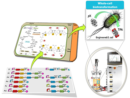 Bio-based p-Xylene Oxidation into Terephthalic Acid by Engineered E.coli
KAIST researchers have established an efficient biocatalytic system to produce terephthalic acid (TPA) from p-xylene (pX). It will allow this industrially important bulk chemical to be made available in a more environmentally-friendly manner.
The research team developed metabolically engineered Escherichia coli (E.coli) to biologically transform pX into TPA, a chemical necessary in the manufacturing of polyethylene terephthalate (PET). This biocatalysis system represents a greener and more efficient alternative to the traditional chemical methods for TPA production. This research, headed by Distinguished Professor Sang Yup Lee, was published in Nature Communications on May 31.
The research team utilized a metabolic engineering and synthetic biology approach to develop a recombinant microorganism that can oxidize pX into TPA using microbial fermentation. TPA is a globally important chemical commodity for manufacturing PET. It can be applied to manufacture plastic bottles, clothing fibers, films, and many other products. Currently, TPA is produced from pX oxidation through an industrially well-known chemical process (with a typical TPA yield of over 95 mol%), which shows, however, such drawbacks as intensive energy requirements at high temperatures and pressure, usage of heavy metal catalysts, and the unavoidable byproduct formation of 4-carboxybenzaldehyde.
The research team designed and constructed a synthetic metabolic pathway by incorporating the upper xylene degradation pathway of Pseudomonas putida F1 and the lower p-toluene sulfonate pathway of Comamonas testosteroni T-2, which successfully produced TPA from pX in small-scale cultures, with the formation of p-toluate (pTA) as the major byproduct. The team further optimized the pathway gene expression levels by using a synthetic biology toolkit, which gave the final engineered E. coli strain showing increased TPA production and the complete elimination of the byproduct.
Using this best-performing strain, the team designed an elegant two-phase (aqueous/organic) fermentation system for TPA production on a larger scale, where pX was supplied in the organic phase. Through a number of optimization steps, the team ultimately achieved production of 13.3 g TPA from 8.8 g pX, which represented an extraordinary yield of 97 mol%.
The team has developed a microbial biotechnology application which is reportedly the first successful example of the bio-based production of TPA from pX by the microbial fermentation of engineered E. coli. This bio-based TPA technology presents several advantages such as ambient reaction temperature and pressure, no use of heavy metals or other toxic chemicals, the removable of byproduct formation, and it is 100% environmentally compatible.
Professor Lee said, “We presented promising biotechnology for producing large amounts of the commodity chemical TPA, which is used for PET manufacturing, through metabolically engineered gut bacterium. Our research is meaningful in that it demonstrates the feasibility of the biotechnological production of bulk chemicals, and if reproducible when up-scaled, it will represent a breakthrough in hydrocarbon bioconversions.”
Ph.D. candidate Zi Wei Luo is the first author of this research (DOI:10.1038/ncomms15689).The research was supported by the Intelligent Synthetic Biology Center through the Global Frontier Project (2011-0031963) of the Ministry of Science, ICT & Future Planning through the National Research Foundation of Korea.
Figure: Biotransformation of pX into TPA by engineered E. coli.
This schematic diagram shows the overall conceptualization of how metabolically engineered E. coli produced TPA from pX. The engineered E. coli was developed through reconstituting a synthetic metabolic pathway for pX conversion to TPA and optimized for increased TPA yield and byproduct elimination. Two-phase partitioning fermentation system was developed for demonstrating the feasibility of large-scale production of TPA from pX using the engineered E. coli strains, where pX was supplied in the organic phase and TPA was produced in the aqueous phase.
2017.06.05 View 12788
Bio-based p-Xylene Oxidation into Terephthalic Acid by Engineered E.coli
KAIST researchers have established an efficient biocatalytic system to produce terephthalic acid (TPA) from p-xylene (pX). It will allow this industrially important bulk chemical to be made available in a more environmentally-friendly manner.
The research team developed metabolically engineered Escherichia coli (E.coli) to biologically transform pX into TPA, a chemical necessary in the manufacturing of polyethylene terephthalate (PET). This biocatalysis system represents a greener and more efficient alternative to the traditional chemical methods for TPA production. This research, headed by Distinguished Professor Sang Yup Lee, was published in Nature Communications on May 31.
The research team utilized a metabolic engineering and synthetic biology approach to develop a recombinant microorganism that can oxidize pX into TPA using microbial fermentation. TPA is a globally important chemical commodity for manufacturing PET. It can be applied to manufacture plastic bottles, clothing fibers, films, and many other products. Currently, TPA is produced from pX oxidation through an industrially well-known chemical process (with a typical TPA yield of over 95 mol%), which shows, however, such drawbacks as intensive energy requirements at high temperatures and pressure, usage of heavy metal catalysts, and the unavoidable byproduct formation of 4-carboxybenzaldehyde.
The research team designed and constructed a synthetic metabolic pathway by incorporating the upper xylene degradation pathway of Pseudomonas putida F1 and the lower p-toluene sulfonate pathway of Comamonas testosteroni T-2, which successfully produced TPA from pX in small-scale cultures, with the formation of p-toluate (pTA) as the major byproduct. The team further optimized the pathway gene expression levels by using a synthetic biology toolkit, which gave the final engineered E. coli strain showing increased TPA production and the complete elimination of the byproduct.
Using this best-performing strain, the team designed an elegant two-phase (aqueous/organic) fermentation system for TPA production on a larger scale, where pX was supplied in the organic phase. Through a number of optimization steps, the team ultimately achieved production of 13.3 g TPA from 8.8 g pX, which represented an extraordinary yield of 97 mol%.
The team has developed a microbial biotechnology application which is reportedly the first successful example of the bio-based production of TPA from pX by the microbial fermentation of engineered E. coli. This bio-based TPA technology presents several advantages such as ambient reaction temperature and pressure, no use of heavy metals or other toxic chemicals, the removable of byproduct formation, and it is 100% environmentally compatible.
Professor Lee said, “We presented promising biotechnology for producing large amounts of the commodity chemical TPA, which is used for PET manufacturing, through metabolically engineered gut bacterium. Our research is meaningful in that it demonstrates the feasibility of the biotechnological production of bulk chemicals, and if reproducible when up-scaled, it will represent a breakthrough in hydrocarbon bioconversions.”
Ph.D. candidate Zi Wei Luo is the first author of this research (DOI:10.1038/ncomms15689).The research was supported by the Intelligent Synthetic Biology Center through the Global Frontier Project (2011-0031963) of the Ministry of Science, ICT & Future Planning through the National Research Foundation of Korea.
Figure: Biotransformation of pX into TPA by engineered E. coli.
This schematic diagram shows the overall conceptualization of how metabolically engineered E. coli produced TPA from pX. The engineered E. coli was developed through reconstituting a synthetic metabolic pathway for pX conversion to TPA and optimized for increased TPA yield and byproduct elimination. Two-phase partitioning fermentation system was developed for demonstrating the feasibility of large-scale production of TPA from pX using the engineered E. coli strains, where pX was supplied in the organic phase and TPA was produced in the aqueous phase.
2017.06.05 View 12788 -
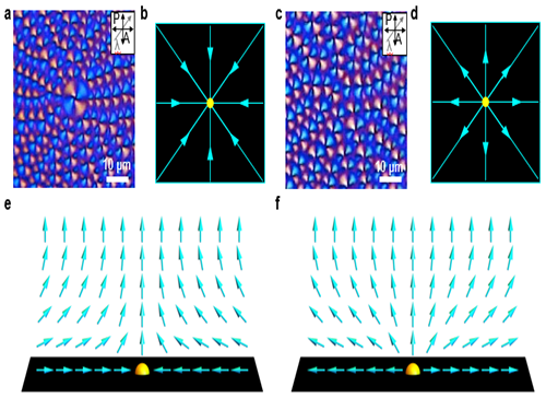 Observation of the Phase Transition of Liquid Crystal Defects
KAIST researchers observed the phase transition of topological defects formed by liquid crystal (LC) materials for the first time.
The phase transition of topological defects, which was also the theme of the Nobel Prize for Physics in 2016, can be difficult to understand for a layperson but it needs to be studied to understand the mysteries of the universe or the underlying physics of skyrmions, which have intrinsic topological defects.
If the galaxy is taken as an example in the universe, it is difficult to observe the topological defects because the system is too large to observe some changes over a limited period of time. In the case of defect structures formed by LC molecules, they are not only a suitable size to observe with an optical microscope, but also the time period in which the phase transition of a defect occurring can be directly observed over a few seconds, which can be extended to a few minutes. The defect structures formed by LC material have radial, circular, or spiral shapes centering on a singularity (defect core), like the singularity that was already introduced in the famous movie "Interstellar,” which is the center point of black hole.
In general, LC materials are mainly used in liquid crystal displays (LCDs) and optical sensors because it is easy to control their specific orientation and they have fast response characteristics and huge anisotropic optical properties. It is advantageous in terms of the performance of LCDs that the defects of the LC materials are minimized. The research team led by Professor Dong Ki Yoon in the Graduate School of Nanoscience and Technology did not simply minimize such defects but actively tried to use the LC defects as building blocks to make micro- and nanostructures for the patterning applications. During these efforts, they found the way to directly study the phase transition of topological defects under in-situ conditions.
Considering the LC material from the viewpoint of a device like a LCD, robustness is important. Therefore, the LC material is injected through the capillary phenomenon between a rigid two-glass plate and the orientation of the LCs can be followed by the surface anchoring condition of the glass substrate. However, in this conventional case, it is difficult to observe the phase transition of the LC defect due to this strong surface anchoring force induced by the solid substrate.
In order to solve this problem, the research team designed a platform, in which the movement of the LC molecules was not restricted, by forming a thin film of LC material on water, which is like oil floating on water. For this, a droplet of LC material was dripped onto water and spread to form a thin film. The topological defects formed under this circumstance could show the thermal phase transition when the temperature was changed. In addition, this approach can trace back the morphology of the original defect structure from the sequential changes during the temperature changes, which can give hints to the study of the formation of topological defects in the cosmos or skyrmions.
Prof. Yoon said, “The study of LC crystal defects itself has been extensively studied by physicists and mathematicians for about 100 years. However, this is the first time that we have observed the phase transition of LC defects directly.” He also added, "Korea is leading in the LCD industry, but our basic research on LCs is not at the world's research level."
The first author of this study is Dr. Min-Jun Gimand supported by a grant from the National Research Foundation (NRF) and funded by the Korean Government (MSIP). The research result was published on May 30, 2017 in Nature Communications.
Figure 1. The phase transition of the LC topological defect on cooling.
Figure 2. Polarizing optical microscopy images of topological defects depending on the strength of the director field. (a,b,e) Convergent director field arrangements of LC molecules and corresponding schematic images; (c,d,f) Divergent director field arrangements of LC molecules and corresponding schematic images.
2017.06.02 View 11024
Observation of the Phase Transition of Liquid Crystal Defects
KAIST researchers observed the phase transition of topological defects formed by liquid crystal (LC) materials for the first time.
The phase transition of topological defects, which was also the theme of the Nobel Prize for Physics in 2016, can be difficult to understand for a layperson but it needs to be studied to understand the mysteries of the universe or the underlying physics of skyrmions, which have intrinsic topological defects.
If the galaxy is taken as an example in the universe, it is difficult to observe the topological defects because the system is too large to observe some changes over a limited period of time. In the case of defect structures formed by LC molecules, they are not only a suitable size to observe with an optical microscope, but also the time period in which the phase transition of a defect occurring can be directly observed over a few seconds, which can be extended to a few minutes. The defect structures formed by LC material have radial, circular, or spiral shapes centering on a singularity (defect core), like the singularity that was already introduced in the famous movie "Interstellar,” which is the center point of black hole.
In general, LC materials are mainly used in liquid crystal displays (LCDs) and optical sensors because it is easy to control their specific orientation and they have fast response characteristics and huge anisotropic optical properties. It is advantageous in terms of the performance of LCDs that the defects of the LC materials are minimized. The research team led by Professor Dong Ki Yoon in the Graduate School of Nanoscience and Technology did not simply minimize such defects but actively tried to use the LC defects as building blocks to make micro- and nanostructures for the patterning applications. During these efforts, they found the way to directly study the phase transition of topological defects under in-situ conditions.
Considering the LC material from the viewpoint of a device like a LCD, robustness is important. Therefore, the LC material is injected through the capillary phenomenon between a rigid two-glass plate and the orientation of the LCs can be followed by the surface anchoring condition of the glass substrate. However, in this conventional case, it is difficult to observe the phase transition of the LC defect due to this strong surface anchoring force induced by the solid substrate.
In order to solve this problem, the research team designed a platform, in which the movement of the LC molecules was not restricted, by forming a thin film of LC material on water, which is like oil floating on water. For this, a droplet of LC material was dripped onto water and spread to form a thin film. The topological defects formed under this circumstance could show the thermal phase transition when the temperature was changed. In addition, this approach can trace back the morphology of the original defect structure from the sequential changes during the temperature changes, which can give hints to the study of the formation of topological defects in the cosmos or skyrmions.
Prof. Yoon said, “The study of LC crystal defects itself has been extensively studied by physicists and mathematicians for about 100 years. However, this is the first time that we have observed the phase transition of LC defects directly.” He also added, "Korea is leading in the LCD industry, but our basic research on LCs is not at the world's research level."
The first author of this study is Dr. Min-Jun Gimand supported by a grant from the National Research Foundation (NRF) and funded by the Korean Government (MSIP). The research result was published on May 30, 2017 in Nature Communications.
Figure 1. The phase transition of the LC topological defect on cooling.
Figure 2. Polarizing optical microscopy images of topological defects depending on the strength of the director field. (a,b,e) Convergent director field arrangements of LC molecules and corresponding schematic images; (c,d,f) Divergent director field arrangements of LC molecules and corresponding schematic images.
2017.06.02 View 11024 -
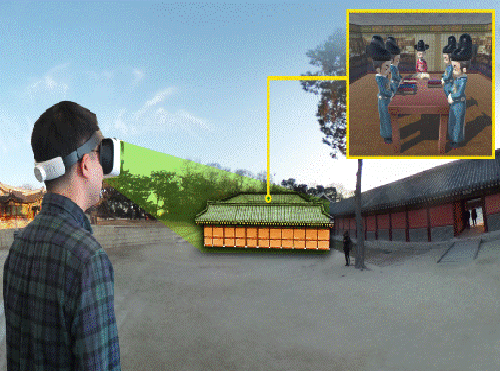 Augmented Reality Application for Smart Tour
‘K-Culture Time Machine,’ an augmented and virtual reality application will create a new way to take a tour. Prof. Woon-taek Woo's research team of Graduate School of Culture Technology of KAIST developed AR/VR application for smart tourism.
The 'K-Culture Time Machine' application (iOS App Store app name: KCTM) was launched on iOS App Store in Korea on May 22 as a pilot service that is targetting the Changdeokgung Palace of Seoul.
The application provides remote experience over time and space for cultural heritage or relics thorough wearable 360-degree video. Users can remotely experience cultural heritage sites with 360-degree video provided by installing a smartphone in a smartphone HMD device, and can search information on historical figures, places, and events related to cultural heritage. Also, 3D reconstruction of lost cultural heritage can be experienced.
Without using wearable HMD devices, mobile-based cultural heritage guides can be provided based on the vision-based recognition on the cultural heritages. Through the embedded camera in smartphone, the application can identify the heritages and provide related information and contents of the hertages. For example, in Changdeokgung Palace, a user can move inside the Changdeokgung Palace from Donhwa-Gate (the main gate of the Changdeokgung Palace), Injeong-Jeon(main hall), Injeong-Moon (Main gate of Injeong-Jeon), and to Huijeongdang (rest place for the king). Through the 360 degree panoramic image or video, the user can experience the virtual scene of heritages.
The virtual 3D reconstruction of the seungjeongwon (Royal Secretariat) which does not exist at present can be shown of the east side of the Injeong-Jeon The functions can be experienced on a smartphone without a wearable device, and it would be a commercial application that can be utilized in the field once the augmented reality function which is under development is completed.
Professor Woo and his research team constructed and applied standardized metadata of cultural heritage database and AR/VR contents. Through this standardized metadata, unlike existing applications which are temporarily consumed after development, reusable and interoperable contents can be made.Professor Woo said, "By enhancing the interoperability and reusability of AR contents, we will be able to preoccupy new markets in the field of smart tourism."
The research was conducted through the joint work with Post Media (CEO Hong Seung-mo) in the CT R&D project of the Ministry of Culture, Sports and Tourism of Korea. The results of the research will be announced through the HCI International 2017 conference in Canada this July.
Figure 1. 360 degree panorama image / video function screen of 'K-Culture Time Machine'. Smartphone HMD allows users to freely experience various cultural sites remotely.
Figure 2. 'K-Culture Time Machine' mobile augmented reality function screen. By analyzing the location of the user and the screen viewed through the camera, information related to the cultural heritage are provided to enhance the user experience.
Figure 3. The concept of 360-degree panoramic video-based VR service of "K-Culture Time Machine", a wearable application supporting smart tour of the historical sites. Through the smartphone HMD, a user can remotely experience cultural heritage sites and 3D reconstruction of cultural heritage that does not currently exist.
2017.05.30 View 12541
Augmented Reality Application for Smart Tour
‘K-Culture Time Machine,’ an augmented and virtual reality application will create a new way to take a tour. Prof. Woon-taek Woo's research team of Graduate School of Culture Technology of KAIST developed AR/VR application for smart tourism.
The 'K-Culture Time Machine' application (iOS App Store app name: KCTM) was launched on iOS App Store in Korea on May 22 as a pilot service that is targetting the Changdeokgung Palace of Seoul.
The application provides remote experience over time and space for cultural heritage or relics thorough wearable 360-degree video. Users can remotely experience cultural heritage sites with 360-degree video provided by installing a smartphone in a smartphone HMD device, and can search information on historical figures, places, and events related to cultural heritage. Also, 3D reconstruction of lost cultural heritage can be experienced.
Without using wearable HMD devices, mobile-based cultural heritage guides can be provided based on the vision-based recognition on the cultural heritages. Through the embedded camera in smartphone, the application can identify the heritages and provide related information and contents of the hertages. For example, in Changdeokgung Palace, a user can move inside the Changdeokgung Palace from Donhwa-Gate (the main gate of the Changdeokgung Palace), Injeong-Jeon(main hall), Injeong-Moon (Main gate of Injeong-Jeon), and to Huijeongdang (rest place for the king). Through the 360 degree panoramic image or video, the user can experience the virtual scene of heritages.
The virtual 3D reconstruction of the seungjeongwon (Royal Secretariat) which does not exist at present can be shown of the east side of the Injeong-Jeon The functions can be experienced on a smartphone without a wearable device, and it would be a commercial application that can be utilized in the field once the augmented reality function which is under development is completed.
Professor Woo and his research team constructed and applied standardized metadata of cultural heritage database and AR/VR contents. Through this standardized metadata, unlike existing applications which are temporarily consumed after development, reusable and interoperable contents can be made.Professor Woo said, "By enhancing the interoperability and reusability of AR contents, we will be able to preoccupy new markets in the field of smart tourism."
The research was conducted through the joint work with Post Media (CEO Hong Seung-mo) in the CT R&D project of the Ministry of Culture, Sports and Tourism of Korea. The results of the research will be announced through the HCI International 2017 conference in Canada this July.
Figure 1. 360 degree panorama image / video function screen of 'K-Culture Time Machine'. Smartphone HMD allows users to freely experience various cultural sites remotely.
Figure 2. 'K-Culture Time Machine' mobile augmented reality function screen. By analyzing the location of the user and the screen viewed through the camera, information related to the cultural heritage are provided to enhance the user experience.
Figure 3. The concept of 360-degree panoramic video-based VR service of "K-Culture Time Machine", a wearable application supporting smart tour of the historical sites. Through the smartphone HMD, a user can remotely experience cultural heritage sites and 3D reconstruction of cultural heritage that does not currently exist.
2017.05.30 View 12541 -
 KAIST Alumni Take a Strong Hold on Tech-Based Startups
Average sales for KAIST alumni startups in 2015 doubled from the previous year to 20.7 billion KRW. They reportedly recorded approximately 37-times higher sales than non-KAIST alumni startups, demonstrating that KAIST is emerging as strong tech-based venture startup incubator.
According to a white paper on the Profile and Performance of KAIST Startups released recently, the number of KAIST startups stood 1,112, of which 877 were founded by alumni (78.9%), 36 by faculty and staff (3.2%), and 199 by those funded by the KAIST Technology Business Incubation Center (17.9%) at the end of 2015.
The total sales of KAIST startups stood at 13.6 trillion KRW in 2015, a 25% increase compared to the previous year. KAIST alumni startups created about 32,400 jobs in that year.
Most KAIST founders majored in engineering (649 people, 71.1%), followed by business (121 people, 13.3%), natural sciences (86, 9.4%), life science and bio engineering (32 people, 3.5%), and liberal arts and convergence science (24 people, 2.6%), making a total of 913 founders, excluding the 199 startups funded by KAIST Technology Business Incubation Center.
By department, most founders come from electrical engineering (148 people, 16.2%), followed by mechanical engineering (135 people, 14.8%), and computer science (114 people, 12.5%).
KAIST startups produced 63 listed companies (1 KOSPI, 51 KOSDAQ, and 11 KONEX), which accounted for 5.7% of the total 1112 startups. This is significantly higher than the average for venture companies (1.1%). It should be noted that the rate is only around 10% for Korean conglomerate-affiliated companies.
At the point of startup establishment, KAIST alumni startup founders were mostly in their 40s (430 people, 40%), followed by their 30s (415 people, 38.6%), 20s (110 people, 10.2%) and 50s (110 people, 10.2%). Around half of the founders were in their 20s and 30s. In particular, the number of founders in their 20s and 30s was around 3.5 times higher in KAIST startups compared to general startups and 1.2 times higher than venture startups.
The average lifespan of KAIST startups is 10.3 years; 276 companies (25%) were established over 16 years ago, 282 companies (25.4%) between 6 and 10 years, 246 companies (22.1%) between 11 and 15 years, and 308 companies (27.7%) less than five years ago. By type of business, startups based on technology accounted for 88.1%; 510 manufacturing companies accounted for 46.2%, followed by 321 information service companies with 29.1%, and 147 science and technology service companies with 13.3%.
By region, 617 companies (55.5%) were located in Seoul and the nearby metropolitan area, followed by 350 companies (31.5%) located in Daejeon.
2017.05.30 View 6907
KAIST Alumni Take a Strong Hold on Tech-Based Startups
Average sales for KAIST alumni startups in 2015 doubled from the previous year to 20.7 billion KRW. They reportedly recorded approximately 37-times higher sales than non-KAIST alumni startups, demonstrating that KAIST is emerging as strong tech-based venture startup incubator.
According to a white paper on the Profile and Performance of KAIST Startups released recently, the number of KAIST startups stood 1,112, of which 877 were founded by alumni (78.9%), 36 by faculty and staff (3.2%), and 199 by those funded by the KAIST Technology Business Incubation Center (17.9%) at the end of 2015.
The total sales of KAIST startups stood at 13.6 trillion KRW in 2015, a 25% increase compared to the previous year. KAIST alumni startups created about 32,400 jobs in that year.
Most KAIST founders majored in engineering (649 people, 71.1%), followed by business (121 people, 13.3%), natural sciences (86, 9.4%), life science and bio engineering (32 people, 3.5%), and liberal arts and convergence science (24 people, 2.6%), making a total of 913 founders, excluding the 199 startups funded by KAIST Technology Business Incubation Center.
By department, most founders come from electrical engineering (148 people, 16.2%), followed by mechanical engineering (135 people, 14.8%), and computer science (114 people, 12.5%).
KAIST startups produced 63 listed companies (1 KOSPI, 51 KOSDAQ, and 11 KONEX), which accounted for 5.7% of the total 1112 startups. This is significantly higher than the average for venture companies (1.1%). It should be noted that the rate is only around 10% for Korean conglomerate-affiliated companies.
At the point of startup establishment, KAIST alumni startup founders were mostly in their 40s (430 people, 40%), followed by their 30s (415 people, 38.6%), 20s (110 people, 10.2%) and 50s (110 people, 10.2%). Around half of the founders were in their 20s and 30s. In particular, the number of founders in their 20s and 30s was around 3.5 times higher in KAIST startups compared to general startups and 1.2 times higher than venture startups.
The average lifespan of KAIST startups is 10.3 years; 276 companies (25%) were established over 16 years ago, 282 companies (25.4%) between 6 and 10 years, 246 companies (22.1%) between 11 and 15 years, and 308 companies (27.7%) less than five years ago. By type of business, startups based on technology accounted for 88.1%; 510 manufacturing companies accounted for 46.2%, followed by 321 information service companies with 29.1%, and 147 science and technology service companies with 13.3%.
By region, 617 companies (55.5%) were located in Seoul and the nearby metropolitan area, followed by 350 companies (31.5%) located in Daejeon.
2017.05.30 View 6907