Intel
-
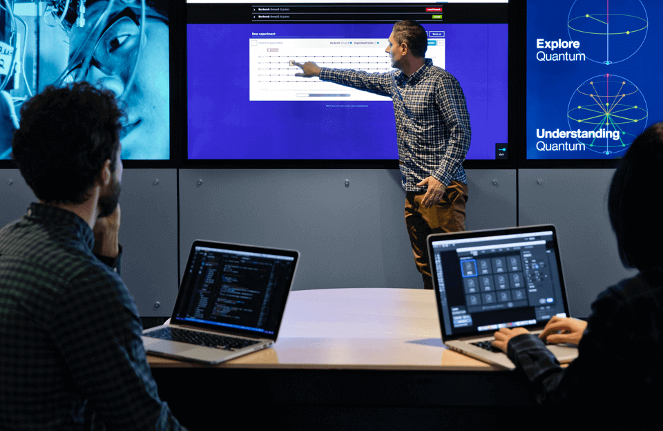 KAIST Joins IBM Q Network to Accelerate Quantum Computing Research and Foster Quantum Industry
KAIST has joined the IBM Q Network, a community of Fortune 500 companies, academic institutions, startups, and research labs working with IBM to advance quantum computing for business and science.
As the IBM Q Network’s first academic partner in Korea, KAIST will use IBM's advanced quantum computing systems to carry out research projects that advance quantum information science and explore early applications. KAIST will also utilize IBM Quantum resources for talent training and education in preparation for building a quantum workforce for the quantum computing era that will bring huge changes to science and business. By joining the network, KAIST will take a leading role in fostering the ecosystem of quantum computing in Korea, which is expected to be a necessary enabler to realize the Fourth Industrial Revolution.
Professor June-Koo Rhee who also serves as Director of the KAIST Information Technology Research Center (ITRC) of Quantum Computing for AI has led the agreement on KAIST’s joining the IBM Q Network. Director Rhee described quantum computing as "a new technology that can calculate mathematical challenges at very high speed and low power” and also as “one that will change the future.”
Director Rhee said, “Korea started investment in quantum computing relatively late, and thus requires to take bold steps with innovative R&D strategies to pave the roadmap for the next technological leap in the field”. With KAIST joining the IBM Q Network, “Korea will be better equipped to establish a quantum industry, an important foundation for securing national competitiveness,” he added.
The KAIST ITRC of Quantum Computing for AI has been using the publicly available IBM Quantum Experience delivered over the IBM Cloud for research, development and training of quantum algorithms such as quantum artificial intelligence, quantum chemical calculation, and quantum computing education.
KAIST will have access to the most advanced IBM Quantum systems to explore practical research and experiments such as diagnosis of diseases based on quantum artificial intelligence, quantum computational chemistry, and quantum machine learning technology. In addition, knowledge exchanges and sharing with overseas universities and companies under the IBM Q Network will help KAIST strengthen the global presence of Korean technology in quantum computing.
About IBM Quantum
IBM Quantum is an industry-first initiative to build quantum systems for business and science applications. For more information about IBM's quantum computing efforts, please visit www.ibm.com/ibmq.
For more information about the IBM Q Network, as well as a full list of all partners, members, and hubs, visit https://www.research.ibm.com/ibm-q/network/
©Thumbnail Image: IBM.
(END)
2020.09.29 View 8980
KAIST Joins IBM Q Network to Accelerate Quantum Computing Research and Foster Quantum Industry
KAIST has joined the IBM Q Network, a community of Fortune 500 companies, academic institutions, startups, and research labs working with IBM to advance quantum computing for business and science.
As the IBM Q Network’s first academic partner in Korea, KAIST will use IBM's advanced quantum computing systems to carry out research projects that advance quantum information science and explore early applications. KAIST will also utilize IBM Quantum resources for talent training and education in preparation for building a quantum workforce for the quantum computing era that will bring huge changes to science and business. By joining the network, KAIST will take a leading role in fostering the ecosystem of quantum computing in Korea, which is expected to be a necessary enabler to realize the Fourth Industrial Revolution.
Professor June-Koo Rhee who also serves as Director of the KAIST Information Technology Research Center (ITRC) of Quantum Computing for AI has led the agreement on KAIST’s joining the IBM Q Network. Director Rhee described quantum computing as "a new technology that can calculate mathematical challenges at very high speed and low power” and also as “one that will change the future.”
Director Rhee said, “Korea started investment in quantum computing relatively late, and thus requires to take bold steps with innovative R&D strategies to pave the roadmap for the next technological leap in the field”. With KAIST joining the IBM Q Network, “Korea will be better equipped to establish a quantum industry, an important foundation for securing national competitiveness,” he added.
The KAIST ITRC of Quantum Computing for AI has been using the publicly available IBM Quantum Experience delivered over the IBM Cloud for research, development and training of quantum algorithms such as quantum artificial intelligence, quantum chemical calculation, and quantum computing education.
KAIST will have access to the most advanced IBM Quantum systems to explore practical research and experiments such as diagnosis of diseases based on quantum artificial intelligence, quantum computational chemistry, and quantum machine learning technology. In addition, knowledge exchanges and sharing with overseas universities and companies under the IBM Q Network will help KAIST strengthen the global presence of Korean technology in quantum computing.
About IBM Quantum
IBM Quantum is an industry-first initiative to build quantum systems for business and science applications. For more information about IBM's quantum computing efforts, please visit www.ibm.com/ibmq.
For more information about the IBM Q Network, as well as a full list of all partners, members, and hubs, visit https://www.research.ibm.com/ibm-q/network/
©Thumbnail Image: IBM.
(END)
2020.09.29 View 8980 -
 Deep Learning Helps Explore the Structural and Strategic Bases of Autism
Psychiatrists typically diagnose autism spectrum disorders (ASD) by observing a person’s behavior and by leaning on the Diagnostic and Statistical Manual of Mental Disorders (DSM-5), widely considered the “bible” of mental health diagnosis.
However, there are substantial differences amongst individuals on the spectrum and a great deal remains unknown by science about the causes of autism, or even what autism is. As a result, an accurate diagnosis of ASD and a prognosis prediction for patients can be extremely difficult.
But what if artificial intelligence (AI) could help? Deep learning, a type of AI, deploys artificial neural networks based on the human brain to recognize patterns in a way that is akin to, and in some cases can surpass, human ability. The technique, or rather suite of techniques, has enjoyed remarkable success in recent years in fields as diverse as voice recognition, translation, autonomous vehicles, and drug discovery.
A group of researchers from KAIST in collaboration with the Yonsei University College of Medicine has applied these deep learning techniques to autism diagnosis. Their findings were published on August 14 in the journal IEEE Access.
Magnetic resonance imaging (MRI) scans of brains of people known to have autism have been used by researchers and clinicians to try to identify structures of the brain they believed were associated with ASD. These researchers have achieved considerable success in identifying abnormal grey and white matter volume and irregularities in cerebral cortex activation and connections as being associated with the condition.
These findings have subsequently been deployed in studies attempting more consistent diagnoses of patients than has been achieved via psychiatrist observations during counseling sessions. While such studies have reported high levels of diagnostic accuracy, the number of participants in these studies has been small, often under 50, and diagnostic performance drops markedly when applied to large sample sizes or on datasets that include people from a wide variety of populations and locations.
“There was something as to what defines autism that human researchers and clinicians must have been overlooking,” said Keun-Ah Cheon, one of the two corresponding authors and a professor in Department of Child and Adolescent Psychiatry at Severance Hospital of the Yonsei University College of Medicine.
“And humans poring over thousands of MRI scans won’t be able to pick up on what we’ve been missing,” she continued. “But we thought AI might be able to.”
So the team applied five different categories of deep learning models to an open-source dataset of more than 1,000 MRI scans from the Autism Brain Imaging Data Exchange (ABIDE) initiative, which has collected brain imaging data from laboratories around the world, and to a smaller, but higher-resolution MRI image dataset (84 images) taken from the Child Psychiatric Clinic at Severance Hospital, Yonsei University College of Medicine. In both cases, the researchers used both structural MRIs (examining the anatomy of the brain) and functional MRIs (examining brain activity in different regions).
The models allowed the team to explore the structural bases of ASD brain region by brain region, focusing in particular on many structures below the cerebral cortex, including the basal ganglia, which are involved in motor function (movement) as well as learning and memory.
Crucially, these specific types of deep learning models also offered up possible explanations of how the AI had come up with its rationale for these findings.
“Understanding the way that the AI has classified these brain structures and dynamics is extremely important,” said Sang Wan Lee, the other corresponding author and an associate professor at KAIST. “It’s no good if a doctor can tell a patient that the computer says they have autism, but not be able to say why the computer knows that.”
The deep learning models were also able to describe how much a particular aspect contributed to ASD, an analysis tool that can assist psychiatric physicians during the diagnosis process to identify the severity of the autism.
“Doctors should be able to use this to offer a personalized diagnosis for patients, including a prognosis of how the condition could develop,” Lee said.
“Artificial intelligence is not going to put psychiatrists out of a job,” he explained. “But using AI as a tool should enable doctors to better understand and diagnose complex disorders than they could do on their own.”
-ProfileProfessor Sang Wan LeeDepartment of Bio and Brain EngineeringLaboratory for Brain and Machine Intelligence https://aibrain.kaist.ac.kr/
KAIST
2020.09.23 View 11380
Deep Learning Helps Explore the Structural and Strategic Bases of Autism
Psychiatrists typically diagnose autism spectrum disorders (ASD) by observing a person’s behavior and by leaning on the Diagnostic and Statistical Manual of Mental Disorders (DSM-5), widely considered the “bible” of mental health diagnosis.
However, there are substantial differences amongst individuals on the spectrum and a great deal remains unknown by science about the causes of autism, or even what autism is. As a result, an accurate diagnosis of ASD and a prognosis prediction for patients can be extremely difficult.
But what if artificial intelligence (AI) could help? Deep learning, a type of AI, deploys artificial neural networks based on the human brain to recognize patterns in a way that is akin to, and in some cases can surpass, human ability. The technique, or rather suite of techniques, has enjoyed remarkable success in recent years in fields as diverse as voice recognition, translation, autonomous vehicles, and drug discovery.
A group of researchers from KAIST in collaboration with the Yonsei University College of Medicine has applied these deep learning techniques to autism diagnosis. Their findings were published on August 14 in the journal IEEE Access.
Magnetic resonance imaging (MRI) scans of brains of people known to have autism have been used by researchers and clinicians to try to identify structures of the brain they believed were associated with ASD. These researchers have achieved considerable success in identifying abnormal grey and white matter volume and irregularities in cerebral cortex activation and connections as being associated with the condition.
These findings have subsequently been deployed in studies attempting more consistent diagnoses of patients than has been achieved via psychiatrist observations during counseling sessions. While such studies have reported high levels of diagnostic accuracy, the number of participants in these studies has been small, often under 50, and diagnostic performance drops markedly when applied to large sample sizes or on datasets that include people from a wide variety of populations and locations.
“There was something as to what defines autism that human researchers and clinicians must have been overlooking,” said Keun-Ah Cheon, one of the two corresponding authors and a professor in Department of Child and Adolescent Psychiatry at Severance Hospital of the Yonsei University College of Medicine.
“And humans poring over thousands of MRI scans won’t be able to pick up on what we’ve been missing,” she continued. “But we thought AI might be able to.”
So the team applied five different categories of deep learning models to an open-source dataset of more than 1,000 MRI scans from the Autism Brain Imaging Data Exchange (ABIDE) initiative, which has collected brain imaging data from laboratories around the world, and to a smaller, but higher-resolution MRI image dataset (84 images) taken from the Child Psychiatric Clinic at Severance Hospital, Yonsei University College of Medicine. In both cases, the researchers used both structural MRIs (examining the anatomy of the brain) and functional MRIs (examining brain activity in different regions).
The models allowed the team to explore the structural bases of ASD brain region by brain region, focusing in particular on many structures below the cerebral cortex, including the basal ganglia, which are involved in motor function (movement) as well as learning and memory.
Crucially, these specific types of deep learning models also offered up possible explanations of how the AI had come up with its rationale for these findings.
“Understanding the way that the AI has classified these brain structures and dynamics is extremely important,” said Sang Wan Lee, the other corresponding author and an associate professor at KAIST. “It’s no good if a doctor can tell a patient that the computer says they have autism, but not be able to say why the computer knows that.”
The deep learning models were also able to describe how much a particular aspect contributed to ASD, an analysis tool that can assist psychiatric physicians during the diagnosis process to identify the severity of the autism.
“Doctors should be able to use this to offer a personalized diagnosis for patients, including a prognosis of how the condition could develop,” Lee said.
“Artificial intelligence is not going to put psychiatrists out of a job,” he explained. “But using AI as a tool should enable doctors to better understand and diagnose complex disorders than they could do on their own.”
-ProfileProfessor Sang Wan LeeDepartment of Bio and Brain EngineeringLaboratory for Brain and Machine Intelligence https://aibrain.kaist.ac.kr/
KAIST
2020.09.23 View 11380 -
 Advanced NVMe Controller Technology for Next Generation Memory Devices
KAIST researchers advanced non-volatile memory express (NVMe) controller technology for next generation information storage devices, and made this new technology named ‘OpenExpress’ freely available to all universities and research institutes around the world to help reduce the research cost in related fields.
NVMe is a communication protocol made for high-performance storage devices based on a peripheral component interconnect-express (PCI-E) interface. NVMe has been developed to take the place of the Serial AT Attachment (SATA) protocol, which was developed to process data on hard disk drives (HDDs) and did not perform well in solid state drives (SSDs).
Unlike HDDs that use magnetic spinning disks, SSDs use semiconductor memory, allowing the rapid reading and writing of data. SSDs also generate less heat and noise, and are much more compact and lightweight.
Since data processing in SSDs using NVMe is up to six times faster than when SATA is used, NVMe has become the standard protocol for ultra-high speed and volume data processing, and is currently used in many flash-based information storage devices.
Studies on NVMe continue at both the academic and industrial levels, however, its poor accessibility is a drawback. Major information and communications technology (ICT) companies around the world expend astronomical costs to procure intellectual property (IP) related to hardware NVMe controllers, necessary for the use of NVMe. However, such IP is not publicly disclosed, making it difficult to be used by universities and research institutes for research purposes.
Although a small number of U.S. Silicon Valley startups provide parts of their independently developed IP for research, the cost of usage is around 34,000 USD per month. The costs skyrocket even further because each copy of single-use source code purchased for IP modification costs approximately 84,000 USD.
In order to address these issues, a group of researchers led by Professor Myoungsoo Jung from the School of Electrical Engineering at KAIST developed a next generation NVMe controller technology that achieved parallel data input/output processing for SSDs in a fully hardware automated form.
The researchers presented their work at the 2020 USENIX Annual Technical Conference (USENIX ATC ’20) in July, and released it as an open research framework named ‘OpenExpress.’
This NVMe controller technology developed by Professor Jung’s team comprises a wide range of basic hardware IP and key NVMe IP cores. To examine its actual performance, the team made an NVMe hardware controller prototype using OpenExpress, and designed all logics provided by OpenExpress to operate at high frequency.
The field-programmable gate array (FPGA) memory card prototype developed using OpenExpress demonstrated increased input/output data processing capacity per second, supporting up to 7 gigabit per second (GB/s) bandwidth. This makes it suitable for ultra-high speed and volume next generation memory device research.
In a test comparing various storage server loads on devices, the team’s FPGA also showed 76% higher bandwidth and 68% lower input/output delay compared to Intel’s new high performance SSD (Optane SSD), which is sufficient for many researchers studying systems employing future memory devices. Depending on user needs, silicon devices can be synthesized as well, which is expected to further enhance performance.
The NVMe controller technology of Professor Jung’s team can be freely used and modified under the OpenExpress open-source end-user agreement for non-commercial use by all universities and research institutes. This makes it extremely useful for research on next-generation memory compatible NVMe controllers and software stacks.
“With the product of this study being disclosed to the world, universities and research institutes can now use controllers that used to be exclusive for only the world’s biggest companies, at no cost,ˮ said Professor Jung. He went on to stress, “This is a meaningful first step in research of information storage device systems such as high-speed and volume next generation memory.”
This work was supported by a grant from MemRay, a company specializing in next generation memory development and distribution.
More details about the study can be found at http://camelab.org.
Image credit: Professor Myoungsoo Jung, KAIST
Image usage restrictions: News organizations may use or redistribute these figures and image, with proper attribution, as part of news coverage of this paper only.
-Publication:
Myoungsoo Jung. (2020). OpenExpress: Fully Hardware Automated Open Research Framework for Future Fast NVMe Devices. Presented in the Proceedings of the 2020 USENIX Annual Technical Conference (USENIX ATC ’20), Available online at https://www.usenix.org/system/files/atc20-jung.pdf
-Profile: Myoungsoo Jung
Associate Professor
m.jung@kaist.ac.kr
http://camelab.org
Computer Architecture and Memory Systems Laboratory
School of Electrical Engineering
http://kaist.ac.kr
Korea Advanced Institute of Science and Technology (KAIST)
Daejeon, Republic of Korea
(END)
2020.09.04 View 11216
Advanced NVMe Controller Technology for Next Generation Memory Devices
KAIST researchers advanced non-volatile memory express (NVMe) controller technology for next generation information storage devices, and made this new technology named ‘OpenExpress’ freely available to all universities and research institutes around the world to help reduce the research cost in related fields.
NVMe is a communication protocol made for high-performance storage devices based on a peripheral component interconnect-express (PCI-E) interface. NVMe has been developed to take the place of the Serial AT Attachment (SATA) protocol, which was developed to process data on hard disk drives (HDDs) and did not perform well in solid state drives (SSDs).
Unlike HDDs that use magnetic spinning disks, SSDs use semiconductor memory, allowing the rapid reading and writing of data. SSDs also generate less heat and noise, and are much more compact and lightweight.
Since data processing in SSDs using NVMe is up to six times faster than when SATA is used, NVMe has become the standard protocol for ultra-high speed and volume data processing, and is currently used in many flash-based information storage devices.
Studies on NVMe continue at both the academic and industrial levels, however, its poor accessibility is a drawback. Major information and communications technology (ICT) companies around the world expend astronomical costs to procure intellectual property (IP) related to hardware NVMe controllers, necessary for the use of NVMe. However, such IP is not publicly disclosed, making it difficult to be used by universities and research institutes for research purposes.
Although a small number of U.S. Silicon Valley startups provide parts of their independently developed IP for research, the cost of usage is around 34,000 USD per month. The costs skyrocket even further because each copy of single-use source code purchased for IP modification costs approximately 84,000 USD.
In order to address these issues, a group of researchers led by Professor Myoungsoo Jung from the School of Electrical Engineering at KAIST developed a next generation NVMe controller technology that achieved parallel data input/output processing for SSDs in a fully hardware automated form.
The researchers presented their work at the 2020 USENIX Annual Technical Conference (USENIX ATC ’20) in July, and released it as an open research framework named ‘OpenExpress.’
This NVMe controller technology developed by Professor Jung’s team comprises a wide range of basic hardware IP and key NVMe IP cores. To examine its actual performance, the team made an NVMe hardware controller prototype using OpenExpress, and designed all logics provided by OpenExpress to operate at high frequency.
The field-programmable gate array (FPGA) memory card prototype developed using OpenExpress demonstrated increased input/output data processing capacity per second, supporting up to 7 gigabit per second (GB/s) bandwidth. This makes it suitable for ultra-high speed and volume next generation memory device research.
In a test comparing various storage server loads on devices, the team’s FPGA also showed 76% higher bandwidth and 68% lower input/output delay compared to Intel’s new high performance SSD (Optane SSD), which is sufficient for many researchers studying systems employing future memory devices. Depending on user needs, silicon devices can be synthesized as well, which is expected to further enhance performance.
The NVMe controller technology of Professor Jung’s team can be freely used and modified under the OpenExpress open-source end-user agreement for non-commercial use by all universities and research institutes. This makes it extremely useful for research on next-generation memory compatible NVMe controllers and software stacks.
“With the product of this study being disclosed to the world, universities and research institutes can now use controllers that used to be exclusive for only the world’s biggest companies, at no cost,ˮ said Professor Jung. He went on to stress, “This is a meaningful first step in research of information storage device systems such as high-speed and volume next generation memory.”
This work was supported by a grant from MemRay, a company specializing in next generation memory development and distribution.
More details about the study can be found at http://camelab.org.
Image credit: Professor Myoungsoo Jung, KAIST
Image usage restrictions: News organizations may use or redistribute these figures and image, with proper attribution, as part of news coverage of this paper only.
-Publication:
Myoungsoo Jung. (2020). OpenExpress: Fully Hardware Automated Open Research Framework for Future Fast NVMe Devices. Presented in the Proceedings of the 2020 USENIX Annual Technical Conference (USENIX ATC ’20), Available online at https://www.usenix.org/system/files/atc20-jung.pdf
-Profile: Myoungsoo Jung
Associate Professor
m.jung@kaist.ac.kr
http://camelab.org
Computer Architecture and Memory Systems Laboratory
School of Electrical Engineering
http://kaist.ac.kr
Korea Advanced Institute of Science and Technology (KAIST)
Daejeon, Republic of Korea
(END)
2020.09.04 View 11216 -
 KAIST Technology Value Tops in Commercialization Market
KAIST became the first Korean university to achieve 10.183 billion KRW in annual technology royalties, and was also selected as an ‘Institution of Outstanding Patent Quality Management’ and an ‘Institution of Outstanding Public Patent Technology Transfer’ for 2020.
KAIST earns its technology royalties through 56 technology transfer contracts. Following KAIST in the rankings were Seoul National University (SNU) in second place with 8.8 billion KRW from 87 contracts and Korea University (KU) in the third with 5.4 billion KRW from 133 contracts. The data shows the high value of KAIST-created technology in the market.
The Korean Intellectual Property Office (KIPO) started to recognize the Institution of Outstanding Patent Quality Management this year to encourage profit-driven patent management at universities and public research institutes, and KAIST was selected as one of the four first recipients of this distinction.
In addition, KAIST was selected as an Institution of Outstanding Public Patent Technology Transfer, a title given by KIPO to three universities and public research institutes this year with outstanding achievements in technology transfers and commercialization to encourage patent utilization.
Director of the KAIST Institute of Technology Value Creation (ITVC) Professor Kyung-cheol Choi said that KAIST’s achievement in annual technology royalties and technology transfers and commercialization were prime examples of accelerating competitiveness in intellectual property through innovative R&D investment.
In April, KAIST expanded and reorganized its Industry-Academia Collaboration Team into the ITVC to support technology transfers and commercialization. Specialized organizations such as the Intellectual Property and Technology Transfer Center and Industrial Liaison Center have been established under the ITVC, and industry experts have been recruited as special professors focusing on industry-academia collaborations to enhance its specialized functions.
KAIST also operates an enterprise membership system and technology consulting system, aimed at sharing its outstanding intellectual property within domestic industries. In 2019, it secured a technology transfer commercialization fund of 1.2 billion KRW available for three years under KIPO’s Intellectual Property Profit Reinvestment Support Program (formerly the Korean Patent Gap Fund Creation Project).
This program was introduced to bridge the gap between the technology developed in universities and the level of technology required by industry. Under the program, bold investments are made in early-stage technologies at the research paper or experiment phase.
The program encourages enterprises to take active steps for the transfer of technologies by demonstrating their commercial potential through prototype production, testing and certification, and standard patent filing. KAIST is currently funding approximately 20 new technologies under this program as of July 2020.
KAIST’s outstanding intellectual property management has also received international recognition, with its selection as Asia’s leading institution in university R&D intellectual property at the Intellectual Property Business Congress (IPBC) Asia 2019 held in Tokyo, Japan last October.
(END)
2020.08.18 View 10265
KAIST Technology Value Tops in Commercialization Market
KAIST became the first Korean university to achieve 10.183 billion KRW in annual technology royalties, and was also selected as an ‘Institution of Outstanding Patent Quality Management’ and an ‘Institution of Outstanding Public Patent Technology Transfer’ for 2020.
KAIST earns its technology royalties through 56 technology transfer contracts. Following KAIST in the rankings were Seoul National University (SNU) in second place with 8.8 billion KRW from 87 contracts and Korea University (KU) in the third with 5.4 billion KRW from 133 contracts. The data shows the high value of KAIST-created technology in the market.
The Korean Intellectual Property Office (KIPO) started to recognize the Institution of Outstanding Patent Quality Management this year to encourage profit-driven patent management at universities and public research institutes, and KAIST was selected as one of the four first recipients of this distinction.
In addition, KAIST was selected as an Institution of Outstanding Public Patent Technology Transfer, a title given by KIPO to three universities and public research institutes this year with outstanding achievements in technology transfers and commercialization to encourage patent utilization.
Director of the KAIST Institute of Technology Value Creation (ITVC) Professor Kyung-cheol Choi said that KAIST’s achievement in annual technology royalties and technology transfers and commercialization were prime examples of accelerating competitiveness in intellectual property through innovative R&D investment.
In April, KAIST expanded and reorganized its Industry-Academia Collaboration Team into the ITVC to support technology transfers and commercialization. Specialized organizations such as the Intellectual Property and Technology Transfer Center and Industrial Liaison Center have been established under the ITVC, and industry experts have been recruited as special professors focusing on industry-academia collaborations to enhance its specialized functions.
KAIST also operates an enterprise membership system and technology consulting system, aimed at sharing its outstanding intellectual property within domestic industries. In 2019, it secured a technology transfer commercialization fund of 1.2 billion KRW available for three years under KIPO’s Intellectual Property Profit Reinvestment Support Program (formerly the Korean Patent Gap Fund Creation Project).
This program was introduced to bridge the gap between the technology developed in universities and the level of technology required by industry. Under the program, bold investments are made in early-stage technologies at the research paper or experiment phase.
The program encourages enterprises to take active steps for the transfer of technologies by demonstrating their commercial potential through prototype production, testing and certification, and standard patent filing. KAIST is currently funding approximately 20 new technologies under this program as of July 2020.
KAIST’s outstanding intellectual property management has also received international recognition, with its selection as Asia’s leading institution in university R&D intellectual property at the Intellectual Property Business Congress (IPBC) Asia 2019 held in Tokyo, Japan last October.
(END)
2020.08.18 View 10265 -
 Education, a Silver Lining in the Dark COVID-19 Cloud
If there is a silver lining behind the COVID-19 pandemic clouds engulfing the world in darkness, it would be ‘education’. The disruption caused by the pandemic has reminded us of the skills that students need in this unpredictable world and raised public awareness of guaranteeing continuous, fair, and quality learning opportunities. Educational innovation can become a positive and powerful catalyst to transform the world for a better future in the post-COVID era.
According to the speakers at the virtual forum co-hosted by the Global Strategy Institute (GSI) and Korea Policy Center for the Fourth Industrial Revolution (KPC4IR) at KAIST on June 24, the recent transition to remote education amplifies the existing socio-economic disparities between the haves and the have-nots, and narrowing the digital divide is the most urgent challenge that should be addressed in this ever-evolving technology-dominating era. They also called for students to be resilient despite the numerous uncertainties ahead of them and prepare new skill sets to better adjust to new environments.
KAIST launched the GSI as its think tank in February of this year. The GSI aims to identify global issues proactively and help make breakthroughs well aligned with solid science and technology-based policies. The second forum of the KAIST GSI, following its inaugural forum in April, was held under the theme “Envisioning the Future of Education for a Non-Contact Society in the Post-Coronavirus Era”.
In his opening remarks, KAIST President Sung-Chul Shin stressed that “distance teaching and learning will eventually become integral components of our future education system”. He then called for close collaboration between the public and private sectors to better shape the future of digital education. President Shin said that global cooperation is also needed to continue offering inclusive, quality education that can equally benefit every student around the world. “We should never let a crisis go to waste, and the COVID-19 pandemic is no exception,” he added.
CEO of Minerva Schools Ben Nelson described the current coronavirus crisis as “an earthquake happening deep down on the ocean floor – we don’t feel it, but it can cause a devastating tsunami.” He continued, “Online learning can totally change the current education system forever.”
Saying that blended education, which combines online and offline classes, will be the new norm in the post-coronavirus era, Coursera CEO Jeff Maggioncalda anticipates that institutions will have to offer more and more online courses and credentials, and should at the same time prepare to drive down the cost of education as students expect to pay much less in tuition and fees for online learning options. “With the economy slumping and unemployment soaring, job-relevant education will also be a must,” Maggioncalda said.
National University of Singapore President Tan Eng Chye further pointed out that future education systems should prepare students to be creative lifelong learners. President Tan encouraged students to be able to integrate knowledge and technical skills from multiple disciplines for complex problem solving, and be adaptable and resilient with bigger appetites for risks and a higher tolerance for failures. He also mentioned digital competency, empathy, and social responsibility as virtues that students in the post-coronavirus era should possess.
Rebecca Winthrop, Co-Director of the Center for Universal Education at the Brookings Institution, raised concerns over the ever-growing digital disparities caused by the recent shift to online teaching and learning, claiming that insufficient infrastructures for low-income families in developing nations are already causing added educational disparities and provoking the inequity issue around the world. “New approaches to leapfrog inequality and provide quality education equally through faster and more effective means should be studied,” she said.
In response to this, Vice President of Microsoft Anthony Salcito introduced the Microsoft Education Transformation Framework, which provides practical advice to develop strategies for digital education transformation with a holistic, long-term view implemented in discrete phases that the global community can begin today. The Framework reportedly shows how emerging technologies, such as artificial intelligence, support new approaches to building efficient and effective physical and digital infrastructure, modernizing teaching and learning, empowering research, and managing student success.
The GSI will host two more forums in September and November.
(END)
2020.06.24 View 14088
Education, a Silver Lining in the Dark COVID-19 Cloud
If there is a silver lining behind the COVID-19 pandemic clouds engulfing the world in darkness, it would be ‘education’. The disruption caused by the pandemic has reminded us of the skills that students need in this unpredictable world and raised public awareness of guaranteeing continuous, fair, and quality learning opportunities. Educational innovation can become a positive and powerful catalyst to transform the world for a better future in the post-COVID era.
According to the speakers at the virtual forum co-hosted by the Global Strategy Institute (GSI) and Korea Policy Center for the Fourth Industrial Revolution (KPC4IR) at KAIST on June 24, the recent transition to remote education amplifies the existing socio-economic disparities between the haves and the have-nots, and narrowing the digital divide is the most urgent challenge that should be addressed in this ever-evolving technology-dominating era. They also called for students to be resilient despite the numerous uncertainties ahead of them and prepare new skill sets to better adjust to new environments.
KAIST launched the GSI as its think tank in February of this year. The GSI aims to identify global issues proactively and help make breakthroughs well aligned with solid science and technology-based policies. The second forum of the KAIST GSI, following its inaugural forum in April, was held under the theme “Envisioning the Future of Education for a Non-Contact Society in the Post-Coronavirus Era”.
In his opening remarks, KAIST President Sung-Chul Shin stressed that “distance teaching and learning will eventually become integral components of our future education system”. He then called for close collaboration between the public and private sectors to better shape the future of digital education. President Shin said that global cooperation is also needed to continue offering inclusive, quality education that can equally benefit every student around the world. “We should never let a crisis go to waste, and the COVID-19 pandemic is no exception,” he added.
CEO of Minerva Schools Ben Nelson described the current coronavirus crisis as “an earthquake happening deep down on the ocean floor – we don’t feel it, but it can cause a devastating tsunami.” He continued, “Online learning can totally change the current education system forever.”
Saying that blended education, which combines online and offline classes, will be the new norm in the post-coronavirus era, Coursera CEO Jeff Maggioncalda anticipates that institutions will have to offer more and more online courses and credentials, and should at the same time prepare to drive down the cost of education as students expect to pay much less in tuition and fees for online learning options. “With the economy slumping and unemployment soaring, job-relevant education will also be a must,” Maggioncalda said.
National University of Singapore President Tan Eng Chye further pointed out that future education systems should prepare students to be creative lifelong learners. President Tan encouraged students to be able to integrate knowledge and technical skills from multiple disciplines for complex problem solving, and be adaptable and resilient with bigger appetites for risks and a higher tolerance for failures. He also mentioned digital competency, empathy, and social responsibility as virtues that students in the post-coronavirus era should possess.
Rebecca Winthrop, Co-Director of the Center for Universal Education at the Brookings Institution, raised concerns over the ever-growing digital disparities caused by the recent shift to online teaching and learning, claiming that insufficient infrastructures for low-income families in developing nations are already causing added educational disparities and provoking the inequity issue around the world. “New approaches to leapfrog inequality and provide quality education equally through faster and more effective means should be studied,” she said.
In response to this, Vice President of Microsoft Anthony Salcito introduced the Microsoft Education Transformation Framework, which provides practical advice to develop strategies for digital education transformation with a holistic, long-term view implemented in discrete phases that the global community can begin today. The Framework reportedly shows how emerging technologies, such as artificial intelligence, support new approaches to building efficient and effective physical and digital infrastructure, modernizing teaching and learning, empowering research, and managing student success.
The GSI will host two more forums in September and November.
(END)
2020.06.24 View 14088 -
 Professor Alice Haeyun Oh to Join GPAI Expert Group
Professor Alice Haeyun Oh will participate in the Global Partnership on Artificial Intelligence (GPAI), an international and multi-stakeholder initiative hosted by the OECD to guide the responsible development and use of AI. In collaboration with partners and international organizations, GPAI will bring together leading experts from industry, civil society, government, and academia.
The Korean Ministry of Science and ICT (MSIT) officially announced that South Korea will take part in GPAI as one of the 15 founding members that include Canada, France, Japan, and the United States.
Professor Oh has been appointed as a new member of the Responsible AI Committee, one of the four committees that GPAI established along with the Data Governance Committee, Future of Work Committee, and Innovation and Commercialization Committee.
(END)
2020.06.22 View 8480
Professor Alice Haeyun Oh to Join GPAI Expert Group
Professor Alice Haeyun Oh will participate in the Global Partnership on Artificial Intelligence (GPAI), an international and multi-stakeholder initiative hosted by the OECD to guide the responsible development and use of AI. In collaboration with partners and international organizations, GPAI will bring together leading experts from industry, civil society, government, and academia.
The Korean Ministry of Science and ICT (MSIT) officially announced that South Korea will take part in GPAI as one of the 15 founding members that include Canada, France, Japan, and the United States.
Professor Oh has been appointed as a new member of the Responsible AI Committee, one of the four committees that GPAI established along with the Data Governance Committee, Future of Work Committee, and Innovation and Commercialization Committee.
(END)
2020.06.22 View 8480 -
 Research on the Million Follower Fallacy Receives the Test of Time Award
Professor Meeyoung Cha’s research investigating the correlation between the number of followers on social media and its influence was re-highlighted after 10 years of publication of the paper.
Saying that her research is still as relevant today as the day it was published 10 years ago, the Association for the Advancement of Artificial Intelligence (AAAI) presented Professor Cha from the School of Computing with the Test of Time Award during the 14th International Conference on Web and Social Media (ICWSM) held online June 8 through 11.
In her 2010 paper titled ‘Measuring User Influence in Twitter: The Million Follower Fallacy,’ Professor Cha proved that number of followers does not match the influential power. She investigated the data including 54,981,152 user accounts, 1,963,263,821 social links, and 1,755,925,520 Tweets, collected with 50 servers.
The research compares and illustrates the limitations of various methods used to measure the influence a user has on a social networking platform. These results provided new insights and interpretations to the influencer selection algorithm used to maximize the advertizing impact on big social networking platforms.
The research also looked at how long an influential user was active for, and whether the user could freely cross the borders between fields and be influential on different topics as well. By analyzing cases of who becomes an influencer when new events occur, it was shown that a person could quickly become an influencer using several key tactics, unlike what was previously claimed by the ‘accidental influential theory’.
Professor Cha explained, “At the time, data from social networking platforms did not receive much attention in computer science, but I remember those all-nighters I pulled to work on this project, fascinated by the fact that internet data could be used to solve difficult social science problems. I feel so grateful that my research has been endeared for such a long time.”
Professor Cha received both her undergraduate and graduate degrees from KAIST, and conducted this research during her postdoctoral course at the Max Planck Institute in Germany. She now also serves as a chief investigator of a data science group at the Institute for Basic Science (IBS).
(END)
2020.06.22 View 7379
Research on the Million Follower Fallacy Receives the Test of Time Award
Professor Meeyoung Cha’s research investigating the correlation between the number of followers on social media and its influence was re-highlighted after 10 years of publication of the paper.
Saying that her research is still as relevant today as the day it was published 10 years ago, the Association for the Advancement of Artificial Intelligence (AAAI) presented Professor Cha from the School of Computing with the Test of Time Award during the 14th International Conference on Web and Social Media (ICWSM) held online June 8 through 11.
In her 2010 paper titled ‘Measuring User Influence in Twitter: The Million Follower Fallacy,’ Professor Cha proved that number of followers does not match the influential power. She investigated the data including 54,981,152 user accounts, 1,963,263,821 social links, and 1,755,925,520 Tweets, collected with 50 servers.
The research compares and illustrates the limitations of various methods used to measure the influence a user has on a social networking platform. These results provided new insights and interpretations to the influencer selection algorithm used to maximize the advertizing impact on big social networking platforms.
The research also looked at how long an influential user was active for, and whether the user could freely cross the borders between fields and be influential on different topics as well. By analyzing cases of who becomes an influencer when new events occur, it was shown that a person could quickly become an influencer using several key tactics, unlike what was previously claimed by the ‘accidental influential theory’.
Professor Cha explained, “At the time, data from social networking platforms did not receive much attention in computer science, but I remember those all-nighters I pulled to work on this project, fascinated by the fact that internet data could be used to solve difficult social science problems. I feel so grateful that my research has been endeared for such a long time.”
Professor Cha received both her undergraduate and graduate degrees from KAIST, and conducted this research during her postdoctoral course at the Max Planck Institute in Germany. She now also serves as a chief investigator of a data science group at the Institute for Basic Science (IBS).
(END)
2020.06.22 View 7379 -
 A Deep-Learned E-Skin Decodes Complex Human Motion
A deep-learning powered single-strained electronic skin sensor can capture human motion from a distance. The single strain sensor placed on the wrist decodes complex five-finger motions in real time with a virtual 3D hand that mirrors the original motions. The deep neural network boosted by rapid situation learning (RSL) ensures stable operation regardless of its position on the surface of the skin.
Conventional approaches require many sensor networks that cover the entire curvilinear surfaces of the target area. Unlike conventional wafer-based fabrication, this laser fabrication provides a new sensing paradigm for motion tracking.
The research team, led by Professor Sungho Jo from the School of Computing, collaborated with Professor Seunghwan Ko from Seoul National University to design this new measuring system that extracts signals corresponding to multiple finger motions by generating cracks in metal nanoparticle films using laser technology. The sensor patch was then attached to a user’s wrist to detect the movement of the fingers.
The concept of this research started from the idea that pinpointing a single area would be more efficient for identifying movements than affixing sensors to every joint and muscle. To make this targeting strategy work, it needs to accurately capture the signals from different areas at the point where they all converge, and then decoupling the information entangled in the converged signals. To maximize users’ usability and mobility, the research team used a single-channeled sensor to generate the signals corresponding to complex hand motions.
The rapid situation learning (RSL) system collects data from arbitrary parts on the wrist and automatically trains the model in a real-time demonstration with a virtual 3D hand that mirrors the original motions. To enhance the sensitivity of the sensor, researchers used laser-induced nanoscale cracking.
This sensory system can track the motion of the entire body with a small sensory network and facilitate the indirect remote measurement of human motions, which is applicable for wearable VR/AR systems.
The research team said they focused on two tasks while developing the sensor. First, they analyzed the sensor signal patterns into a latent space encapsulating temporal sensor behavior and then they mapped the latent vectors to finger motion metric spaces.
Professor Jo said, “Our system is expandable to other body parts. We already confirmed that the sensor is also capable of extracting gait motions from a pelvis. This technology is expected to provide a turning point in health-monitoring, motion tracking, and soft robotics.”
This study was featured in Nature Communications.
Publication:
Kim, K. K., et al. (2020) A deep-learned skin sensor decoding the epicentral human motions. Nature Communications. 11. 2149. https://doi.org/10.1038/s41467-020-16040-y29
Link to download the full-text paper:
https://www.nature.com/articles/s41467-020-16040-y.pdf
Profile: Professor Sungho Jo
shjo@kaist.ac.kr
http://nmail.kaist.ac.kr
Neuro-Machine Augmented Intelligence Lab
School of Computing
College of Engineering
KAIST
2020.06.10 View 12556
A Deep-Learned E-Skin Decodes Complex Human Motion
A deep-learning powered single-strained electronic skin sensor can capture human motion from a distance. The single strain sensor placed on the wrist decodes complex five-finger motions in real time with a virtual 3D hand that mirrors the original motions. The deep neural network boosted by rapid situation learning (RSL) ensures stable operation regardless of its position on the surface of the skin.
Conventional approaches require many sensor networks that cover the entire curvilinear surfaces of the target area. Unlike conventional wafer-based fabrication, this laser fabrication provides a new sensing paradigm for motion tracking.
The research team, led by Professor Sungho Jo from the School of Computing, collaborated with Professor Seunghwan Ko from Seoul National University to design this new measuring system that extracts signals corresponding to multiple finger motions by generating cracks in metal nanoparticle films using laser technology. The sensor patch was then attached to a user’s wrist to detect the movement of the fingers.
The concept of this research started from the idea that pinpointing a single area would be more efficient for identifying movements than affixing sensors to every joint and muscle. To make this targeting strategy work, it needs to accurately capture the signals from different areas at the point where they all converge, and then decoupling the information entangled in the converged signals. To maximize users’ usability and mobility, the research team used a single-channeled sensor to generate the signals corresponding to complex hand motions.
The rapid situation learning (RSL) system collects data from arbitrary parts on the wrist and automatically trains the model in a real-time demonstration with a virtual 3D hand that mirrors the original motions. To enhance the sensitivity of the sensor, researchers used laser-induced nanoscale cracking.
This sensory system can track the motion of the entire body with a small sensory network and facilitate the indirect remote measurement of human motions, which is applicable for wearable VR/AR systems.
The research team said they focused on two tasks while developing the sensor. First, they analyzed the sensor signal patterns into a latent space encapsulating temporal sensor behavior and then they mapped the latent vectors to finger motion metric spaces.
Professor Jo said, “Our system is expandable to other body parts. We already confirmed that the sensor is also capable of extracting gait motions from a pelvis. This technology is expected to provide a turning point in health-monitoring, motion tracking, and soft robotics.”
This study was featured in Nature Communications.
Publication:
Kim, K. K., et al. (2020) A deep-learned skin sensor decoding the epicentral human motions. Nature Communications. 11. 2149. https://doi.org/10.1038/s41467-020-16040-y29
Link to download the full-text paper:
https://www.nature.com/articles/s41467-020-16040-y.pdf
Profile: Professor Sungho Jo
shjo@kaist.ac.kr
http://nmail.kaist.ac.kr
Neuro-Machine Augmented Intelligence Lab
School of Computing
College of Engineering
KAIST
2020.06.10 View 12556 -
 Professor Dongsu Han Named Program Chair for ACM CoNEXT 2020
Professor Dongsu Han from the School of Electrical Engineering has been appointed as the program chair for the 16th Association for Computing Machinery’s International Conference on emerging Networking EXperiments and Technologies (ACM CoNEXT 2020). Professor Han is the first program chair to be appointed from an Asian institution.
ACM CoNEXT is hosted by ACM SIGCOMM, ACM's Special Interest Group on Data Communications, which specializes in the field of communication and computer networks.
Professor Han will serve as program co-chair along with Professor Anja Feldmann from the Max Planck Institute for Informatics. Together, they have appointed 40 world-leading researchers as program committee members for this conference, including Professor Song Min Kim from KAIST School of Electrical Engineering.
Paper submissions for the conference can be made by the end of June, and the event itself is to take place from the 1st to 4th of December.
Conference Website: https://conferences2.sigcomm.org/co-next/2020/#!/home
(END)
2020.06.02 View 10475
Professor Dongsu Han Named Program Chair for ACM CoNEXT 2020
Professor Dongsu Han from the School of Electrical Engineering has been appointed as the program chair for the 16th Association for Computing Machinery’s International Conference on emerging Networking EXperiments and Technologies (ACM CoNEXT 2020). Professor Han is the first program chair to be appointed from an Asian institution.
ACM CoNEXT is hosted by ACM SIGCOMM, ACM's Special Interest Group on Data Communications, which specializes in the field of communication and computer networks.
Professor Han will serve as program co-chair along with Professor Anja Feldmann from the Max Planck Institute for Informatics. Together, they have appointed 40 world-leading researchers as program committee members for this conference, including Professor Song Min Kim from KAIST School of Electrical Engineering.
Paper submissions for the conference can be made by the end of June, and the event itself is to take place from the 1st to 4th of December.
Conference Website: https://conferences2.sigcomm.org/co-next/2020/#!/home
(END)
2020.06.02 View 10475 -
 Professor Sue-Hyun Lee Listed Among WEF 2020 Young Scientists
Professor Sue-Hyun Lee from the Department of Bio and Brain Engineering joined the World Economic Forum (WEF)’s Young Scientists Community on May 26. The class of 2020 comprises 25 leading researchers from 14 countries across the world who are at the forefront of scientific problem-solving and social change. Professor Lee was the only Korean on this year’s roster.
The WEF created the Young Scientists Community in 2008 to engage leaders from the public and private sectors with science and the role it plays in society. The WEF selects rising-star academics, 40 and under, from various fields every year, and helps them become stronger ambassadors for science, especially in tackling pressing global challenges including cybersecurity, climate change, poverty, and pandemics.
Professor Lee is researching how memories are encoded, recalled, and updated, and how emotional processes affect human memory, in order to ultimately direct the development of therapeutic methods to treat mental disorders. She has made significant contributions to resolving ongoing debates over the maintenance and changes of memory traces in the brain.
In recognition of her research excellence, leadership, and commitment to serving society, the President and the Dean of the College of Engineering at KAIST nominated Professor Lee to the WEF’s Class of 2020 Young Scientists Selection Committee. The Committee also acknowledged Professor Lee’s achievements and potential for expanding the boundaries of knowledge and practical applications of science, and accepted her into the Community.
During her three-year membership in the Community, Professor Lee will be committed to participating in WEF-initiated activities and events related to promising therapeutic interventions for mental disorders and future directions of artificial intelligence.
Seven of this year’s WEF Young Scientists are from Asia, including Professor Lee, while eight are based in Europe. Six study in the Americas, two work in South Africa, and the remaining two in the Middle East. Fourteen, more than half, of the newly announced 25 Young Scientists are women.
(END)
2020.05.26 View 12264
Professor Sue-Hyun Lee Listed Among WEF 2020 Young Scientists
Professor Sue-Hyun Lee from the Department of Bio and Brain Engineering joined the World Economic Forum (WEF)’s Young Scientists Community on May 26. The class of 2020 comprises 25 leading researchers from 14 countries across the world who are at the forefront of scientific problem-solving and social change. Professor Lee was the only Korean on this year’s roster.
The WEF created the Young Scientists Community in 2008 to engage leaders from the public and private sectors with science and the role it plays in society. The WEF selects rising-star academics, 40 and under, from various fields every year, and helps them become stronger ambassadors for science, especially in tackling pressing global challenges including cybersecurity, climate change, poverty, and pandemics.
Professor Lee is researching how memories are encoded, recalled, and updated, and how emotional processes affect human memory, in order to ultimately direct the development of therapeutic methods to treat mental disorders. She has made significant contributions to resolving ongoing debates over the maintenance and changes of memory traces in the brain.
In recognition of her research excellence, leadership, and commitment to serving society, the President and the Dean of the College of Engineering at KAIST nominated Professor Lee to the WEF’s Class of 2020 Young Scientists Selection Committee. The Committee also acknowledged Professor Lee’s achievements and potential for expanding the boundaries of knowledge and practical applications of science, and accepted her into the Community.
During her three-year membership in the Community, Professor Lee will be committed to participating in WEF-initiated activities and events related to promising therapeutic interventions for mental disorders and future directions of artificial intelligence.
Seven of this year’s WEF Young Scientists are from Asia, including Professor Lee, while eight are based in Europe. Six study in the Americas, two work in South Africa, and the remaining two in the Middle East. Fourteen, more than half, of the newly announced 25 Young Scientists are women.
(END)
2020.05.26 View 12264 -
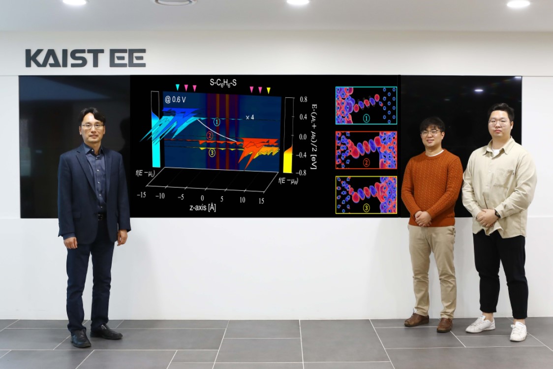 A Theoretical Boost to Nano-Scale Devices
- Researchers calculate the quasi-Fermi levels in molecular junctions applying an initio approach. -
Semiconductor companies are struggling to develop devices that are mere nanometers in size, and much of the challenge lies in being able to more accurately describe the underlying physics at that nano-scale. But a new computational approach that has been in the works for a decade could break down these barriers.
Devices using semiconductors, from computers to solar cells, have enjoyed tremendous efficiency improvements in the last few decades. Famously, one of the co-founders of Intel, Gordon Moore, observed that the number of transistors in an integrated circuit doubles about every two years—and this ‘Moore’s law’ held true for some time.
In recent years, however, such gains have slowed as firms that attempt to engineer nano-scale transistors hit the limits of miniaturization at the atomic level.
Researchers with the School of Electrical Engineering at KAIST have developed a new approach to the underlying physics of semiconductors.
“With open quantum systems as the main research target of our lab, we were revisiting concepts that had been taken for granted and even appear in standard semiconductor physics textbooks such as the voltage drop in operating semiconductor devices,” said the lead researcher Professor Yong-Hoon Kim. “Questioning how all these concepts could be understood and possibly revised at the nano-scale, it was clear that there was something incomplete about our current understanding.”
“And as the semiconductor chips are being scaled down to the atomic level, coming up with a better theory to describe semiconductor devices has become an urgent task.”
The current understanding states that semiconductors are materials that act like half-way houses between conductors, like copper or steel, and insulators, like rubber or Styrofoam. They sometimes conduct electricity, but not always. This makes them a great material for intentionally controlling the flow of current, which in turn is useful for constructing the simple on/off switches—transistors—that are the foundation of memory and logic devices in computers.
In order to ‘switch on’ a semiconductor, a current or light source is applied, exciting an electron in an atom to jump from what is called a ‘valence band,’ which is filled with electrons, up to the ‘conduction band,’ which is originally unfilled or only partially filled with electrons. Electrons that have jumped up to the conduction band thanks to external stimuli and the remaining ‘holes’ are now able to move about and act as charge carriers to flow electric current.
The physical concept that describes the populations of the electrons in the conduction band and the holes in the valence band and the energy required to make this jump is formulated in terms of the so-called ‘Fermi level.’ For example, you need to know the Fermi levels of the electrons and holes in order to know what amount of energy you are going to get out of a solar cell, including losses.
But the Fermi level concept is only straightforwardly defined so long as a semiconductor device is at equilibrium—sitting on a shelf doing nothing—and the whole point of semiconductor devices is not to leave them on the shelf.
Some 70 years ago, William Shockley, the Nobel Prize-winning co-inventor of the transistor at the Bell Labs, came up with a bit of a theoretical fudge, the ‘quasi-Fermi level,’ or QFL, enabling rough prediction and measurement of the interaction between valence band holes and conduction band electrons, and this has worked pretty well until now.
“But when you are working at the scale of just a few nanometers, the methods to theoretically calculate or experimentally measure the splitting of QFLs were just not available,” said Professor Kim.
This means that at this scale, issues such as errors relating to voltage drop take on much greater significance.
Kim’s team worked for nearly ten years on developing a novel theoretical description of nano-scale quantum electron transport that can replace the standard method—and the software that allows them to put it to use. This involved the further development of a bit of math known as the Density Functional Theory that simplifies the equations describing the interactions of electrons, and which has been very useful in other fields such as high-throughput computational materials discovery.
For the first time, they were able to calculate the QFL splitting, offering a new understanding of the relationship between voltage drop and quantum electron transport in atomic scale devices.
In addition to looking into various interesting non-equilibrium quantum phenomena with their novel methodology, the team is now further developing their software into a computer-aided design tool to be used by semiconductor companies for developing and fabricating advanced semiconductor devices.
The study, featured at the Proceedings of the National Academy of Sciences of the USA on May 12, was supported by the National Research Foundation and the Korea Institute of Science and Technology Information Supercomputing Center.
Image caption: The newly developed formalism and QFL splitting analysis led to new ways of characterizing extremely scaled-down semiconductor devices and the technology computer-aided design (TCAD) of next- generation nano-electronic/energy/bio devices.
Image credit: Yong-Hoon Kim, KAIST
Image usage restrictions: News organizations may use or redistribute this image, with proper attribution, as part of news coverage of this paper only.
Publication:
Juho Lee, Hyeonwoo Yeo, and Yong-Hoon Kim. (2020) ‘Quasi-Fermi level splitting in nanoscale junctions from ab initio.’ Proceedings of the National Academy of Sciences of the United States of America (PNAS), Volume 117, Issue 19, pp.10142-101488. Available online at https://doi.org/10.1073/pnas.1921273117
Profile:
Yong-Hoon Kim
Professor
y.h.kim@kaist.ac.kr
http://nanocore.kaist.ac.kr/
1st-Principles Nano-Device Computing Lab
School of Electrical Engineering
KAIST
(END)
2020.05.15 View 8965
A Theoretical Boost to Nano-Scale Devices
- Researchers calculate the quasi-Fermi levels in molecular junctions applying an initio approach. -
Semiconductor companies are struggling to develop devices that are mere nanometers in size, and much of the challenge lies in being able to more accurately describe the underlying physics at that nano-scale. But a new computational approach that has been in the works for a decade could break down these barriers.
Devices using semiconductors, from computers to solar cells, have enjoyed tremendous efficiency improvements in the last few decades. Famously, one of the co-founders of Intel, Gordon Moore, observed that the number of transistors in an integrated circuit doubles about every two years—and this ‘Moore’s law’ held true for some time.
In recent years, however, such gains have slowed as firms that attempt to engineer nano-scale transistors hit the limits of miniaturization at the atomic level.
Researchers with the School of Electrical Engineering at KAIST have developed a new approach to the underlying physics of semiconductors.
“With open quantum systems as the main research target of our lab, we were revisiting concepts that had been taken for granted and even appear in standard semiconductor physics textbooks such as the voltage drop in operating semiconductor devices,” said the lead researcher Professor Yong-Hoon Kim. “Questioning how all these concepts could be understood and possibly revised at the nano-scale, it was clear that there was something incomplete about our current understanding.”
“And as the semiconductor chips are being scaled down to the atomic level, coming up with a better theory to describe semiconductor devices has become an urgent task.”
The current understanding states that semiconductors are materials that act like half-way houses between conductors, like copper or steel, and insulators, like rubber or Styrofoam. They sometimes conduct electricity, but not always. This makes them a great material for intentionally controlling the flow of current, which in turn is useful for constructing the simple on/off switches—transistors—that are the foundation of memory and logic devices in computers.
In order to ‘switch on’ a semiconductor, a current or light source is applied, exciting an electron in an atom to jump from what is called a ‘valence band,’ which is filled with electrons, up to the ‘conduction band,’ which is originally unfilled or only partially filled with electrons. Electrons that have jumped up to the conduction band thanks to external stimuli and the remaining ‘holes’ are now able to move about and act as charge carriers to flow electric current.
The physical concept that describes the populations of the electrons in the conduction band and the holes in the valence band and the energy required to make this jump is formulated in terms of the so-called ‘Fermi level.’ For example, you need to know the Fermi levels of the electrons and holes in order to know what amount of energy you are going to get out of a solar cell, including losses.
But the Fermi level concept is only straightforwardly defined so long as a semiconductor device is at equilibrium—sitting on a shelf doing nothing—and the whole point of semiconductor devices is not to leave them on the shelf.
Some 70 years ago, William Shockley, the Nobel Prize-winning co-inventor of the transistor at the Bell Labs, came up with a bit of a theoretical fudge, the ‘quasi-Fermi level,’ or QFL, enabling rough prediction and measurement of the interaction between valence band holes and conduction band electrons, and this has worked pretty well until now.
“But when you are working at the scale of just a few nanometers, the methods to theoretically calculate or experimentally measure the splitting of QFLs were just not available,” said Professor Kim.
This means that at this scale, issues such as errors relating to voltage drop take on much greater significance.
Kim’s team worked for nearly ten years on developing a novel theoretical description of nano-scale quantum electron transport that can replace the standard method—and the software that allows them to put it to use. This involved the further development of a bit of math known as the Density Functional Theory that simplifies the equations describing the interactions of electrons, and which has been very useful in other fields such as high-throughput computational materials discovery.
For the first time, they were able to calculate the QFL splitting, offering a new understanding of the relationship between voltage drop and quantum electron transport in atomic scale devices.
In addition to looking into various interesting non-equilibrium quantum phenomena with their novel methodology, the team is now further developing their software into a computer-aided design tool to be used by semiconductor companies for developing and fabricating advanced semiconductor devices.
The study, featured at the Proceedings of the National Academy of Sciences of the USA on May 12, was supported by the National Research Foundation and the Korea Institute of Science and Technology Information Supercomputing Center.
Image caption: The newly developed formalism and QFL splitting analysis led to new ways of characterizing extremely scaled-down semiconductor devices and the technology computer-aided design (TCAD) of next- generation nano-electronic/energy/bio devices.
Image credit: Yong-Hoon Kim, KAIST
Image usage restrictions: News organizations may use or redistribute this image, with proper attribution, as part of news coverage of this paper only.
Publication:
Juho Lee, Hyeonwoo Yeo, and Yong-Hoon Kim. (2020) ‘Quasi-Fermi level splitting in nanoscale junctions from ab initio.’ Proceedings of the National Academy of Sciences of the United States of America (PNAS), Volume 117, Issue 19, pp.10142-101488. Available online at https://doi.org/10.1073/pnas.1921273117
Profile:
Yong-Hoon Kim
Professor
y.h.kim@kaist.ac.kr
http://nanocore.kaist.ac.kr/
1st-Principles Nano-Device Computing Lab
School of Electrical Engineering
KAIST
(END)
2020.05.15 View 8965 -
 Professor Jong Chul Ye Appointed as Distinguished Lecturer of IEEE EMBS
Professor Jong Chul Ye from the Department of Bio and Brain Engineering was appointed as a distinguished lecturer by the International Association of Electrical and Electronic Engineers (IEEE) Engineering in Medicine and Biology Society (EMBS). Professor Ye was invited to deliver a lecture on his leading research on artificial intelligence (AI) technology in medical video restoration. He will serve a term of two years beginning in 2020.
IEEE EMBS's distinguished lecturer program is designed to educate researchers around the world on the latest trends and technology in biomedical engineering. Sponsored by IEEE, its members can attend lectures on the distinguished professor's research subject.
Professor Ye said, "We are at a time where the importance of AI in medical imaging is increasing.” He added, “I am proud to be appointed as a distinguished lecturer of the IEEE EMBS in recognition of my contributions to this field.”
(END)
2020.02.27 View 10697
Professor Jong Chul Ye Appointed as Distinguished Lecturer of IEEE EMBS
Professor Jong Chul Ye from the Department of Bio and Brain Engineering was appointed as a distinguished lecturer by the International Association of Electrical and Electronic Engineers (IEEE) Engineering in Medicine and Biology Society (EMBS). Professor Ye was invited to deliver a lecture on his leading research on artificial intelligence (AI) technology in medical video restoration. He will serve a term of two years beginning in 2020.
IEEE EMBS's distinguished lecturer program is designed to educate researchers around the world on the latest trends and technology in biomedical engineering. Sponsored by IEEE, its members can attend lectures on the distinguished professor's research subject.
Professor Ye said, "We are at a time where the importance of AI in medical imaging is increasing.” He added, “I am proud to be appointed as a distinguished lecturer of the IEEE EMBS in recognition of my contributions to this field.”
(END)
2020.02.27 View 10697