Nano
-
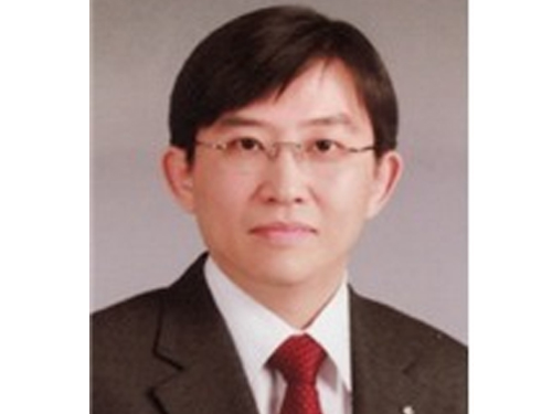 Professor Sang Ouk Kim receives the 2014 Prime Minister Award for Nano Research
Professor Sang Ouk Kim
Sang Ouk Kim, a professor of Materials Science and Engineering at KAIST, received the 2014 Prime Minister Award from the Korean government for his nano research. The award ceremony, Nano Korea 2014, was held on July 2, 2014 at Coex in Seoul, Korea.
Professor Kim was recognized for his research on the control of various shapes of ultra-fine nano-structures using molecular assembly with ductile materials, such as polymers and carbon nano materials, and for his contribution to the growth of the nano field in Korea.
He developed a new molecular assembly control technology, for the first time in the world, which produced large-scale, ultra-fine nanopatterns through controlling the molecular arrangement of block copolymers. Using this technology, he further created a new semiconductor nanotechnology to reinforce the existing lithographic process of semiconductor manufacturing.
In addition, Professor Kim has focused on making a new type of three-dimensional carbon nano-materials by assembling carbon nanotubes or graphene at the molecular level. Developing a new process to produce nano-materials through the chemical doping process of carbon materials, which can be widely applied to solar cells or energy devices, is one of his research interests as well.
Professor Kim has published a total of 124 papers in international journals, such as Nature, Science, Nature Materials, Nature Communications, Advanced Materials, and Nano Letters. He was recently invited by Advanced Materials to contribute a review article for its 25th anniversary issue.
Professor Kim received both the KAIST Academic Award and the 13th Young Scientist Award of Korea in 2010. Since March 2014, he has served as one of the chair professors of KAIST.
Most recently, he was selected as the Scientist of the Month in June 2014 by the Ministry of Science, ICT and Future Planning, Republic of Korea, and the National Research Foundation of Korea.
2014.07.08 View 10343
Professor Sang Ouk Kim receives the 2014 Prime Minister Award for Nano Research
Professor Sang Ouk Kim
Sang Ouk Kim, a professor of Materials Science and Engineering at KAIST, received the 2014 Prime Minister Award from the Korean government for his nano research. The award ceremony, Nano Korea 2014, was held on July 2, 2014 at Coex in Seoul, Korea.
Professor Kim was recognized for his research on the control of various shapes of ultra-fine nano-structures using molecular assembly with ductile materials, such as polymers and carbon nano materials, and for his contribution to the growth of the nano field in Korea.
He developed a new molecular assembly control technology, for the first time in the world, which produced large-scale, ultra-fine nanopatterns through controlling the molecular arrangement of block copolymers. Using this technology, he further created a new semiconductor nanotechnology to reinforce the existing lithographic process of semiconductor manufacturing.
In addition, Professor Kim has focused on making a new type of three-dimensional carbon nano-materials by assembling carbon nanotubes or graphene at the molecular level. Developing a new process to produce nano-materials through the chemical doping process of carbon materials, which can be widely applied to solar cells or energy devices, is one of his research interests as well.
Professor Kim has published a total of 124 papers in international journals, such as Nature, Science, Nature Materials, Nature Communications, Advanced Materials, and Nano Letters. He was recently invited by Advanced Materials to contribute a review article for its 25th anniversary issue.
Professor Kim received both the KAIST Academic Award and the 13th Young Scientist Award of Korea in 2010. Since March 2014, he has served as one of the chair professors of KAIST.
Most recently, he was selected as the Scientist of the Month in June 2014 by the Ministry of Science, ICT and Future Planning, Republic of Korea, and the National Research Foundation of Korea.
2014.07.08 View 10343 -
 Professor Sang Ouk Kim Receives the "Scientist of the Month Award" from the Korean Government
Professor Sang Ouk Kim of the Department of Materials Science and Engineering, KAIST, received the Scientist of the Month Award in June 2014 for his development of a fundamental technology that allows free control of the properties of carbon-based materials.
Since June 1997, the Korean government has awarded monthly one scientist working in industry, universities, or research institutions to recognize his or her research achievements, as well as to promote science and technology.
Professor Kim implemented a technique known as doping, which has been used in ordinary semiconductor processes, to demonstrate the physical properties of carbon-based materials. Carbon nanotubes, graphene, and other carbon materials have superior mechanical and electrical properties and are regarded as next-generation materials. However, difficulty in controlling their qualities has made applications in various devices unfavorable. The doping technique in semiconductor production is to artificially introduce impurities into an extremely pure semiconductor for the purpose of modulating its electrical properties.
Profess Kim doped elements like nitrogen and boron to enable minute control of the physical properties of carbon-based materials and applied the technique to development of organic solar cells, organic light-emitting devices, and flexible memory. He also increased the application range by using a self-assembly method to change freely the structure of carbon-based materials.
Professor Kim has published 53 papers in renowned journals such as Advanced Materials and Nanoletters. He was rewarded further by being invited to write a review paper for the 25th anniversary special edition for Advanced Materials.
2014.06.19 View 11521
Professor Sang Ouk Kim Receives the "Scientist of the Month Award" from the Korean Government
Professor Sang Ouk Kim of the Department of Materials Science and Engineering, KAIST, received the Scientist of the Month Award in June 2014 for his development of a fundamental technology that allows free control of the properties of carbon-based materials.
Since June 1997, the Korean government has awarded monthly one scientist working in industry, universities, or research institutions to recognize his or her research achievements, as well as to promote science and technology.
Professor Kim implemented a technique known as doping, which has been used in ordinary semiconductor processes, to demonstrate the physical properties of carbon-based materials. Carbon nanotubes, graphene, and other carbon materials have superior mechanical and electrical properties and are regarded as next-generation materials. However, difficulty in controlling their qualities has made applications in various devices unfavorable. The doping technique in semiconductor production is to artificially introduce impurities into an extremely pure semiconductor for the purpose of modulating its electrical properties.
Profess Kim doped elements like nitrogen and boron to enable minute control of the physical properties of carbon-based materials and applied the technique to development of organic solar cells, organic light-emitting devices, and flexible memory. He also increased the application range by using a self-assembly method to change freely the structure of carbon-based materials.
Professor Kim has published 53 papers in renowned journals such as Advanced Materials and Nanoletters. He was rewarded further by being invited to write a review paper for the 25th anniversary special edition for Advanced Materials.
2014.06.19 View 11521 -
 Professor Sang-Ouk Kim's Research on Carbon Materials Featured in a Philippines Science News
The subject article said that Professor Sang-Ouk Kim of Materials Science Engineering at KAIST “developed a technique to change the nature of the next-generation carbon-based materials. His research has expanded the possibility of carbon-based materials to be used in clothes.”
For details, please refer to the article below:
Centrio Times, June 10, 2014
KAIST scientist develops color changing carbon materials that can be used in clothes
http://www.centriotimes.com/2014/06/kaist-scientist-develops-color-changing-carbon-materials-can-used-clothes.html.
2014.06.15 View 9026
Professor Sang-Ouk Kim's Research on Carbon Materials Featured in a Philippines Science News
The subject article said that Professor Sang-Ouk Kim of Materials Science Engineering at KAIST “developed a technique to change the nature of the next-generation carbon-based materials. His research has expanded the possibility of carbon-based materials to be used in clothes.”
For details, please refer to the article below:
Centrio Times, June 10, 2014
KAIST scientist develops color changing carbon materials that can be used in clothes
http://www.centriotimes.com/2014/06/kaist-scientist-develops-color-changing-carbon-materials-can-used-clothes.html.
2014.06.15 View 9026 -
 Clear Display Technology Under Sunlight Developed
The late Professor Seung-Man Yang
The last paper of the late Professor Seung-Man Yang, who was a past master of colloids and fluid mechanics
Practical patterning technology of the next generation optical materials, photonic crystals
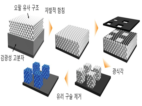
The mineral opal does not possess any pigments, but it appears colorful to our eyes. This is because only a particular wavelength is reflected due to the regular nano-structure of its surface. The material that causes selective reflection of the light is called photonic crystals.
The deceased Professor Seung-Man Yang and his research team from KAIST’s Chemical and Biomolecular Engineering Department ha ve developed micro-pattern technology using photolithographic process. This can accelerate the commercialization of photonic crystals, which is hailed as the next generation optics material.
The research results were published in the April 16th edition of Advanced Materials, known as the most prestigious world-renowned journal in the field of materials science.
The newly developed photonic crystal micro-pattern could be used as a core material for the next generation reflective display that is clearly visible even under sunlight. Since it does not require a separate light source, a single charge is enough to last for several days.
Until now, many scientists have endeavored to make photonic crystals artificially, however, most were produced in a lump and therefore lacked efficiency. Also, the low mechanical stability of the formed structure prevented from commercialization.
In order to solve these problems, the research team has copied the nano-structure of opals.
Glass beads were arranged in the same nano-structure as the opal on top of the photoresist material undergoing photocuring by ultraviolet light. The glass beads were installed in the photoresist materials, and UV light was selectively exposed on micro regions. The remaining region was developed by photolithographic process to successfully produce photonic crystals in micro-patterns.
The co-author of the research, KAIST Chemical and Biomolecular Engineering Department’s Professor Sin-Hyeon Kim, said, “Combining the semiconductor process technology with photonic crystal pattern technology can secure the practical applications for photonic crystals.”He also predicted “This technology can be used as the key optical material that configures the next generation reflective color display device with very low power consumption.”
The late Professor Seung-Man Yang was a world-renowned expert in the field of colloids and fluid mechanics. Professor Yang published over 193 papers in international journals and continued his research until his passing in last September.
He received Du Pont Science and Technology Award in 2007, KAIST Person of the Year 2008, Gyeong-Am Academy Award in 2009, as well as the President’s Award of the Republic of Korea in March 2014. The researchers devoted the achievement of this year’s research to Professor Yang in his honor.
Research was conducted by KAIST Photonic-fluidic Integrated Devices Research Team, as a part of the Creative Research Program funded by the Ministry of Science, ICT and Future Planning, Republic of Korea.
Figure 1. Opal [left] and the nano glass bead arrangement structure within the opal [right]
Figure 2. Process chart of the photonic crystal micro-pattern formation based on photolithography
Figure 3. Opal structure [left] and inverted structure of the opal [right]
Figure 4. Photonic crystal micro-pattern in solid colors
Figure 5. Photonic crystal micro-pattern that reflects two different crystals (Red, Green) [left] and pixelated pattern of photonic crystal in three primary colors (Red, Green, Blue) [right] that is applicable to reflective displays
2014.05.14 View 14011
Clear Display Technology Under Sunlight Developed
The late Professor Seung-Man Yang
The last paper of the late Professor Seung-Man Yang, who was a past master of colloids and fluid mechanics
Practical patterning technology of the next generation optical materials, photonic crystals
The mineral opal does not possess any pigments, but it appears colorful to our eyes. This is because only a particular wavelength is reflected due to the regular nano-structure of its surface. The material that causes selective reflection of the light is called photonic crystals.
The deceased Professor Seung-Man Yang and his research team from KAIST’s Chemical and Biomolecular Engineering Department ha ve developed micro-pattern technology using photolithographic process. This can accelerate the commercialization of photonic crystals, which is hailed as the next generation optics material.
The research results were published in the April 16th edition of Advanced Materials, known as the most prestigious world-renowned journal in the field of materials science.
The newly developed photonic crystal micro-pattern could be used as a core material for the next generation reflective display that is clearly visible even under sunlight. Since it does not require a separate light source, a single charge is enough to last for several days.
Until now, many scientists have endeavored to make photonic crystals artificially, however, most were produced in a lump and therefore lacked efficiency. Also, the low mechanical stability of the formed structure prevented from commercialization.
In order to solve these problems, the research team has copied the nano-structure of opals.
Glass beads were arranged in the same nano-structure as the opal on top of the photoresist material undergoing photocuring by ultraviolet light. The glass beads were installed in the photoresist materials, and UV light was selectively exposed on micro regions. The remaining region was developed by photolithographic process to successfully produce photonic crystals in micro-patterns.
The co-author of the research, KAIST Chemical and Biomolecular Engineering Department’s Professor Sin-Hyeon Kim, said, “Combining the semiconductor process technology with photonic crystal pattern technology can secure the practical applications for photonic crystals.”He also predicted “This technology can be used as the key optical material that configures the next generation reflective color display device with very low power consumption.”
The late Professor Seung-Man Yang was a world-renowned expert in the field of colloids and fluid mechanics. Professor Yang published over 193 papers in international journals and continued his research until his passing in last September.
He received Du Pont Science and Technology Award in 2007, KAIST Person of the Year 2008, Gyeong-Am Academy Award in 2009, as well as the President’s Award of the Republic of Korea in March 2014. The researchers devoted the achievement of this year’s research to Professor Yang in his honor.
Research was conducted by KAIST Photonic-fluidic Integrated Devices Research Team, as a part of the Creative Research Program funded by the Ministry of Science, ICT and Future Planning, Republic of Korea.
Figure 1. Opal [left] and the nano glass bead arrangement structure within the opal [right]
Figure 2. Process chart of the photonic crystal micro-pattern formation based on photolithography
Figure 3. Opal structure [left] and inverted structure of the opal [right]
Figure 4. Photonic crystal micro-pattern in solid colors
Figure 5. Photonic crystal micro-pattern that reflects two different crystals (Red, Green) [left] and pixelated pattern of photonic crystal in three primary colors (Red, Green, Blue) [right] that is applicable to reflective displays
2014.05.14 View 14011 -
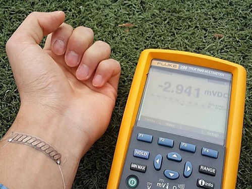 Thermoelectric generator on glass fabric for wearable electronic devices
Wearable computers or devices have been hailed as the next generation of mobile electronic gadgets, from smart watches to smart glasses to smart pacemakers. For electronics to be worn by a user, they must be light, flexible, and equipped with a power source, which could be a portable, long-lasting battery or no battery at all but a generator. How to supply power in a stable and reliable manner is one of the most critical issues to commercialize wearable devices.
A team of KAIST researchers headed by Byung Jin Cho, a professor of electrical engineering, proposed a solution to this problem by developing a glass fabric-based thermoelectric (TE) generator that is extremely light and flexible and produces electricity from the heat of the human body. In fact, it is so flexible that the allowable bending radius of the generator is as low as 20 mm. There are no changes in performance even if the generator bends upward and downward for up to 120 cycles.
To date, two types of TE generators have been developed based either on organic or inorganic materials. The organic-based TE generators use polymers that are highly flexible and compatible with human skin, ideal for wearable electronics. The polymers, however, have a low power output. Inorganic-based TE generators produce a high electrical energy, but they are heavy, rigid, and bulky.
Professor Cho came up with a new concept and design technique to build a flexible TE generator that minimizes thermal energy loss but maximizes power output. His team synthesized liquid-like pastes of n-type (Bi2Te3) and p-type (Sb2Te3) TE materials and printed them onto a glass fabric by applying a screen printing technique. The pastes permeated through the meshes of the fabric and formed films of TE materials in a range of thickness of several hundreds of microns. As a result, hundreds of TE material dots (in combination of n and p types) were printed and well arranged on a specific area of the glass fabric.
Professor Cho explained that his TE generator has a self-sustaining structure, eliminating thick external substrates (usually made of ceramic or alumina) that hold inorganic TE materials. These substrates have taken away a great portion of thermal energy, a serious setback which causes low output power.
He also commented,
"For our case, the glass fabric itself serves as the upper and lower substrates of a TE generator, keeping the inorganic TE materials in between. This is quite a revolutionary approach to design a generator. In so doing, we were able to significantly reduce the weight of our generator (~0.13g/cm2), which is an essential element for wearable electronics."
When using KAIST's TE generator (with a size of 10 cm x 10 cm) for a wearable wristband device, it will produce around 40 mW electric power based on the temperature difference of 31 °F between human skin and the surrounding air.
Professor Cho further described about the merits of the new generator:
"Our technology presents an easy and simple way of fabricating an extremely flexible, light, and high-performance TE generator. We expect that this technology will find further applications in scale-up systems such as automobiles, factories, aircrafts, and vessels where we see abundant thermal energy being wasted."
This research result was published online in the March 14th issue of Energy & Environmental Science and was entitled "Wearable Thermoelectric Generator Fabricated on Glass Fabric."
Youtube Link: http://www.youtube.com/watch?v=BlN9lvEzCuw&feature=youtu.be
[Picture Captions]
Caption 1: The picture shows a high-performance wearable thermoelectric generator that is extremely flexible and light.
Caption 2: A thermoelectric generator developed as a wristband. The generator can be easily curved along with the shape of human body.
Caption 3: KAIST’s thermoelectric generator can be bent as many as 120 times, but it still shows the same high performance.
2014.04.21 View 21523
Thermoelectric generator on glass fabric for wearable electronic devices
Wearable computers or devices have been hailed as the next generation of mobile electronic gadgets, from smart watches to smart glasses to smart pacemakers. For electronics to be worn by a user, they must be light, flexible, and equipped with a power source, which could be a portable, long-lasting battery or no battery at all but a generator. How to supply power in a stable and reliable manner is one of the most critical issues to commercialize wearable devices.
A team of KAIST researchers headed by Byung Jin Cho, a professor of electrical engineering, proposed a solution to this problem by developing a glass fabric-based thermoelectric (TE) generator that is extremely light and flexible and produces electricity from the heat of the human body. In fact, it is so flexible that the allowable bending radius of the generator is as low as 20 mm. There are no changes in performance even if the generator bends upward and downward for up to 120 cycles.
To date, two types of TE generators have been developed based either on organic or inorganic materials. The organic-based TE generators use polymers that are highly flexible and compatible with human skin, ideal for wearable electronics. The polymers, however, have a low power output. Inorganic-based TE generators produce a high electrical energy, but they are heavy, rigid, and bulky.
Professor Cho came up with a new concept and design technique to build a flexible TE generator that minimizes thermal energy loss but maximizes power output. His team synthesized liquid-like pastes of n-type (Bi2Te3) and p-type (Sb2Te3) TE materials and printed them onto a glass fabric by applying a screen printing technique. The pastes permeated through the meshes of the fabric and formed films of TE materials in a range of thickness of several hundreds of microns. As a result, hundreds of TE material dots (in combination of n and p types) were printed and well arranged on a specific area of the glass fabric.
Professor Cho explained that his TE generator has a self-sustaining structure, eliminating thick external substrates (usually made of ceramic or alumina) that hold inorganic TE materials. These substrates have taken away a great portion of thermal energy, a serious setback which causes low output power.
He also commented,
"For our case, the glass fabric itself serves as the upper and lower substrates of a TE generator, keeping the inorganic TE materials in between. This is quite a revolutionary approach to design a generator. In so doing, we were able to significantly reduce the weight of our generator (~0.13g/cm2), which is an essential element for wearable electronics."
When using KAIST's TE generator (with a size of 10 cm x 10 cm) for a wearable wristband device, it will produce around 40 mW electric power based on the temperature difference of 31 °F between human skin and the surrounding air.
Professor Cho further described about the merits of the new generator:
"Our technology presents an easy and simple way of fabricating an extremely flexible, light, and high-performance TE generator. We expect that this technology will find further applications in scale-up systems such as automobiles, factories, aircrafts, and vessels where we see abundant thermal energy being wasted."
This research result was published online in the March 14th issue of Energy & Environmental Science and was entitled "Wearable Thermoelectric Generator Fabricated on Glass Fabric."
Youtube Link: http://www.youtube.com/watch?v=BlN9lvEzCuw&feature=youtu.be
[Picture Captions]
Caption 1: The picture shows a high-performance wearable thermoelectric generator that is extremely flexible and light.
Caption 2: A thermoelectric generator developed as a wristband. The generator can be easily curved along with the shape of human body.
Caption 3: KAIST’s thermoelectric generator can be bent as many as 120 times, but it still shows the same high performance.
2014.04.21 View 21523 -
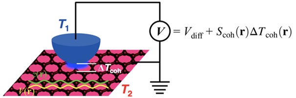 An Electron Cloud Distribution Observed by the Scanning Seebeck Microscope
All matters are made of small particles, namely atoms. An atom is composed of a heavy nucleus and cloud-like, extremely light electrons.
Korean researchers developed an electron microscopy technique that enables the accurate observation of an electron cloud distribution at room-temperature. The achievement is comparable to the invention of the quantum tunneling microscopy technique developed 33 years ago.
Professor Yong-Hyun Kim of the Graduate School of Nanoscience and Technology at KAIST and Dr. Ho-Gi Yeo of the Korea Research Institute of Standards and Science (KRISS) developed the Scanning Seebeck Microscope (SSM). The SSM renders clear images of atoms, as well as an electron cloud distribution. This was achieved by creating a voltage difference via a temperature gradient.
The development was introduced in the online edition of Physical Review Letters (April 2014), a prestigious journal published by the American Institute of Physics.
The SSM is expected to be economically competitive as it gives high resolution images at an atomic scale even for graphene and semiconductors, both at room temperature. In addition, if the SSM is applied to thermoelectric material research, it will contribute to the development of high-efficiency thermoelectric materials.
Through numerous hypotheses and experiments, scientists now believe that there exists an electron cloud surrounding a nucleus. IBM's Scanning Tunneling Microscope (STM) was the first to observe the electron cloud and has remained as the only technique to this day. The developers of IBM microscope, Dr. Gerd Binnig and Dr. Heinrich Rohrer, were awarded the 1986 Nobel Prize in Physics.
There still remains a downside to the STM technique, however: it required high precision and extreme low temperature and vibration. The application of voltage also affects the electron cloud, resulting in a distorted image.
The KAIST research team adopted a different approach by using the Seebeck effect which refers to the voltage generation due to a temperature gradient between two materials.
The team placed an observation sample (graphene) at room temperature (37~57℃) and detected its voltage generation. This technique made it possible to observe an electron cloud at room temperature.
Furthermore, the research team investigated the theoretical quantum mechanics behind the electron cloud using the observation gained through the Seebeck effect and also obtained by simulation capability to analyze the experimental results.
The research was a joint research project between KAIST Professor Yong-Hyun Kim and KRISS researcher Dr. Ho-Gi Yeo. Eui-Seop Lee, a Ph.D. candidate of KAIST, and KRISS researcher Dr. Sang-Hui Cho also participated. The Ministry of Science, ICT, and Future Planning, the Global Frontier Initiative, and the Disruptive Convergent Technology Development Initiative funded the project in Korea.
Picture 1: Schematic Diagram of the Scanning Seebeck Microscope (SSM)
Picture 2: Electron cloud distribution observed by SSM at room temperature
Picture 3: Professor Yong-Hyun Kim
2014.04.04 View 16448
An Electron Cloud Distribution Observed by the Scanning Seebeck Microscope
All matters are made of small particles, namely atoms. An atom is composed of a heavy nucleus and cloud-like, extremely light electrons.
Korean researchers developed an electron microscopy technique that enables the accurate observation of an electron cloud distribution at room-temperature. The achievement is comparable to the invention of the quantum tunneling microscopy technique developed 33 years ago.
Professor Yong-Hyun Kim of the Graduate School of Nanoscience and Technology at KAIST and Dr. Ho-Gi Yeo of the Korea Research Institute of Standards and Science (KRISS) developed the Scanning Seebeck Microscope (SSM). The SSM renders clear images of atoms, as well as an electron cloud distribution. This was achieved by creating a voltage difference via a temperature gradient.
The development was introduced in the online edition of Physical Review Letters (April 2014), a prestigious journal published by the American Institute of Physics.
The SSM is expected to be economically competitive as it gives high resolution images at an atomic scale even for graphene and semiconductors, both at room temperature. In addition, if the SSM is applied to thermoelectric material research, it will contribute to the development of high-efficiency thermoelectric materials.
Through numerous hypotheses and experiments, scientists now believe that there exists an electron cloud surrounding a nucleus. IBM's Scanning Tunneling Microscope (STM) was the first to observe the electron cloud and has remained as the only technique to this day. The developers of IBM microscope, Dr. Gerd Binnig and Dr. Heinrich Rohrer, were awarded the 1986 Nobel Prize in Physics.
There still remains a downside to the STM technique, however: it required high precision and extreme low temperature and vibration. The application of voltage also affects the electron cloud, resulting in a distorted image.
The KAIST research team adopted a different approach by using the Seebeck effect which refers to the voltage generation due to a temperature gradient between two materials.
The team placed an observation sample (graphene) at room temperature (37~57℃) and detected its voltage generation. This technique made it possible to observe an electron cloud at room temperature.
Furthermore, the research team investigated the theoretical quantum mechanics behind the electron cloud using the observation gained through the Seebeck effect and also obtained by simulation capability to analyze the experimental results.
The research was a joint research project between KAIST Professor Yong-Hyun Kim and KRISS researcher Dr. Ho-Gi Yeo. Eui-Seop Lee, a Ph.D. candidate of KAIST, and KRISS researcher Dr. Sang-Hui Cho also participated. The Ministry of Science, ICT, and Future Planning, the Global Frontier Initiative, and the Disruptive Convergent Technology Development Initiative funded the project in Korea.
Picture 1: Schematic Diagram of the Scanning Seebeck Microscope (SSM)
Picture 2: Electron cloud distribution observed by SSM at room temperature
Picture 3: Professor Yong-Hyun Kim
2014.04.04 View 16448 -
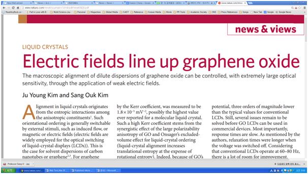 Professor Sang-Ouk Kim Publishes Review Article in the Journal of "Nature Materials"
Nature Materials, a
peer-reviewed scientific journal published by Nature Publishing Group, covers a
range of topics within materials science from materials engineering and
structural materials. The
journal invited Professor Sang-Ouk Kim of Materials Science and Engineering at
KAIST to contribute to the April issue of 2014. Professor Kim,
together with his doctoral student, Ju-Young Kim, wrote a review article in the
“News and Views” section of the journal, which was entitled “Liquid Crystals:
Electric Fields Line Up Graphene Oxide.” The
News and Views is a peer-reviewed section where an academic authority in a particular
field reviews and evaluates papers published in the journal. In
the article, Professor Kim reviewed a paper written by Jang-Kun Song et al. and
highlighted important research outcomes such as the efficient electric field switching
of graphene oxide (GO) liquid-crystals in low-concentration dispersions and the
demonstration of a prototype of a GO liquid-crystal display. This technology
could lead the development of a flexible display. Professor
Kim is an eminent scholar who has reported for the first time in the world on
the solvent-based graphene oxide liquid crystals formation in 2011. For the article, please go to: http://www.kaist.ac.kr/_prog/download.php?filename=Nature_Materials_Professor_Sang-Ouk_Kim_Apr_2014.pdf
2014.03.26 View 10902
Professor Sang-Ouk Kim Publishes Review Article in the Journal of "Nature Materials"
Nature Materials, a
peer-reviewed scientific journal published by Nature Publishing Group, covers a
range of topics within materials science from materials engineering and
structural materials. The
journal invited Professor Sang-Ouk Kim of Materials Science and Engineering at
KAIST to contribute to the April issue of 2014. Professor Kim,
together with his doctoral student, Ju-Young Kim, wrote a review article in the
“News and Views” section of the journal, which was entitled “Liquid Crystals:
Electric Fields Line Up Graphene Oxide.” The
News and Views is a peer-reviewed section where an academic authority in a particular
field reviews and evaluates papers published in the journal. In
the article, Professor Kim reviewed a paper written by Jang-Kun Song et al. and
highlighted important research outcomes such as the efficient electric field switching
of graphene oxide (GO) liquid-crystals in low-concentration dispersions and the
demonstration of a prototype of a GO liquid-crystal display. This technology
could lead the development of a flexible display. Professor
Kim is an eminent scholar who has reported for the first time in the world on
the solvent-based graphene oxide liquid crystals formation in 2011. For the article, please go to: http://www.kaist.ac.kr/_prog/download.php?filename=Nature_Materials_Professor_Sang-Ouk_Kim_Apr_2014.pdf
2014.03.26 View 10902 -
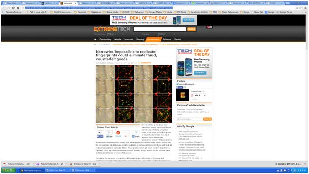 Extreme Tech: Nanowire "impossible to replicate" fingerprints could eliminate fraud, counterfeit goods
Research done by Professor Hyun-Joon Song of Chemistry at KAIST on
anti-counterfeit, nanoscale fingerprints generated by randomly distributed
nanowires was introduced by Extreme Tech, an online global science and technology
news.
For the articles, please go to:
Extreme Tech, March 25, 2014Nanowire ‘impossible to replicate’ fingerprints could eliminate fraud, counterfeit goods
http://www.extremetech.com/extreme/179131-nanowire-impossible-to-replicate-fingerprints-could-eliminate-fraud-counterfeit-goods
2014.03.26 View 9784
Extreme Tech: Nanowire "impossible to replicate" fingerprints could eliminate fraud, counterfeit goods
Research done by Professor Hyun-Joon Song of Chemistry at KAIST on
anti-counterfeit, nanoscale fingerprints generated by randomly distributed
nanowires was introduced by Extreme Tech, an online global science and technology
news.
For the articles, please go to:
Extreme Tech, March 25, 2014Nanowire ‘impossible to replicate’ fingerprints could eliminate fraud, counterfeit goods
http://www.extremetech.com/extreme/179131-nanowire-impossible-to-replicate-fingerprints-could-eliminate-fraud-counterfeit-goods
2014.03.26 View 9784 -
 Professor Kyung-Wook Paik Receives the Best Presentation Award from 2014 Pan Pacific Symposium
The Surface Mount Technology Association (SMTA) hosted its 19th Annual Pan Pacific Microelectronics Symposium on February 11-13, 2014 in Hawaii.
The 2014 conference, promoting international technical exchange and extensive networking among microelectronics professionals from around the world, presented over 50 papers from 17 countries.
Professor Kyung-Wook Paik of Materials Science Engineering at KAIST received the Best Presentation Award for his paper titled, “Novel Nanofiber Anisotropic Films for Nine Pitch Assembly” at the conference.
SMTA is an international network of professionals in electronics assembly technologies, including Microsystems, emerging technologies, and related business operations.
2014.03.17 View 10627
Professor Kyung-Wook Paik Receives the Best Presentation Award from 2014 Pan Pacific Symposium
The Surface Mount Technology Association (SMTA) hosted its 19th Annual Pan Pacific Microelectronics Symposium on February 11-13, 2014 in Hawaii.
The 2014 conference, promoting international technical exchange and extensive networking among microelectronics professionals from around the world, presented over 50 papers from 17 countries.
Professor Kyung-Wook Paik of Materials Science Engineering at KAIST received the Best Presentation Award for his paper titled, “Novel Nanofiber Anisotropic Films for Nine Pitch Assembly” at the conference.
SMTA is an international network of professionals in electronics assembly technologies, including Microsystems, emerging technologies, and related business operations.
2014.03.17 View 10627 -
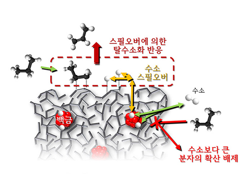 Spillover Phenomenon Identified Using Model Catalyst System
Researchers at KAIST have identified spillover phenomenon, which has remained controversial since its discovery in the early 1960s.
KAIST Department of Chemical and Biomolecular Engineering’s Professor Min-Gi Choi and his team has explained the "spillover phenomenon," using their own model catalyst system where platinum is selectively located within the amorphous aluminosilicate.
The research results were published on the 25th February online edition of Nature Communications.
Spillover refers to a phenomenon that occurs when hydrogen atoms that have been activated on the surface of metals, such as platinum, move to the surface of the catalyst. It was predicted that this phenomenon can be used to design a catalyst with high activity and stability, and thus has been actively studied over the last 50 years.
However, many cases of the known catalysts involved competing reactions on the exposed metal surface, which made it impossible to directly identify the presence and formation mechanism of spillover.
The catalysts developed by the researchers at KAIST used platinum nanoparticles covered with aluminosilicate. This only allowed the hydrogen molecules to pass through and has effectively blocked the competing reactions, enabling the research team to study the spillover phenomenon.
Through various catalyst structure and reactivity analysis, as well as computer modeling, the team has discovered that Brönsted acid sites present on the aluminosilicate plays a crucial role in spillover phenomenon.
In addition, the spillover-based hydrogenation catalyst proposed by the research team showed very high hydrogenation and dehydrogenation activity. The ability of the catalyst to significantly inhibit unwanted hydrogenolysis reaction during the petrochemical processes also suggested a large industrial potential.
Professor Min-Gi Choi said, “This particular catalyst, which can trigger the reaction only by spillover phenomenon, can be properly designed to exceed the capacity of the conventional metal catalysts. The future goal is to make a catalyst with much higher activity and selectivity.”
The research was conducted through funds subsidized by SK Innovation and Ministry of Science, ICT and Future Planning.
The senior research fellow of SK Innovation Seung-Hun Oh said, “SK Innovation will continue to develop a new commercial catalyst based on the technology from this research.”
Juh-Wan Lim and Hye-Yeong Shin led the research as joint first authors under supervision of Professor Min-Gi Choi and computer modeling works were conducted by KAIST EEWS (environment, energy, water, and sustainability) graduate school’s Professor Hyeong-Jun Kim.
2014.03.03 View 11448
Spillover Phenomenon Identified Using Model Catalyst System
Researchers at KAIST have identified spillover phenomenon, which has remained controversial since its discovery in the early 1960s.
KAIST Department of Chemical and Biomolecular Engineering’s Professor Min-Gi Choi and his team has explained the "spillover phenomenon," using their own model catalyst system where platinum is selectively located within the amorphous aluminosilicate.
The research results were published on the 25th February online edition of Nature Communications.
Spillover refers to a phenomenon that occurs when hydrogen atoms that have been activated on the surface of metals, such as platinum, move to the surface of the catalyst. It was predicted that this phenomenon can be used to design a catalyst with high activity and stability, and thus has been actively studied over the last 50 years.
However, many cases of the known catalysts involved competing reactions on the exposed metal surface, which made it impossible to directly identify the presence and formation mechanism of spillover.
The catalysts developed by the researchers at KAIST used platinum nanoparticles covered with aluminosilicate. This only allowed the hydrogen molecules to pass through and has effectively blocked the competing reactions, enabling the research team to study the spillover phenomenon.
Through various catalyst structure and reactivity analysis, as well as computer modeling, the team has discovered that Brönsted acid sites present on the aluminosilicate plays a crucial role in spillover phenomenon.
In addition, the spillover-based hydrogenation catalyst proposed by the research team showed very high hydrogenation and dehydrogenation activity. The ability of the catalyst to significantly inhibit unwanted hydrogenolysis reaction during the petrochemical processes also suggested a large industrial potential.
Professor Min-Gi Choi said, “This particular catalyst, which can trigger the reaction only by spillover phenomenon, can be properly designed to exceed the capacity of the conventional metal catalysts. The future goal is to make a catalyst with much higher activity and selectivity.”
The research was conducted through funds subsidized by SK Innovation and Ministry of Science, ICT and Future Planning.
The senior research fellow of SK Innovation Seung-Hun Oh said, “SK Innovation will continue to develop a new commercial catalyst based on the technology from this research.”
Juh-Wan Lim and Hye-Yeong Shin led the research as joint first authors under supervision of Professor Min-Gi Choi and computer modeling works were conducted by KAIST EEWS (environment, energy, water, and sustainability) graduate school’s Professor Hyeong-Jun Kim.
2014.03.03 View 11448 -
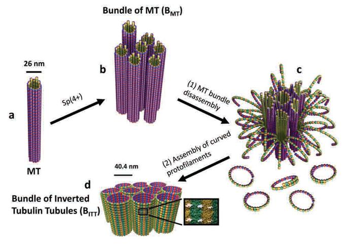 A Molecular Switch Controlling Self-Assembly of Protein Nanotubes Discovered
International collaborative research among South Korea, United States, and Israel research institutionsThe key to the treatment of cancer and brain disease mechanism The molecular switch that controls the self-assembly structure of the protein nanotubes, which plays crucial role in cell division and intracellular transport of materials, has been discovered. KAIST Bio and Brain Engineering Department’s Professor Myeong-Cheol Choi and Professor Chae-Yeon Song conducted the research, in collaboration with the University of California in Santa Barbara, U.S., and Hebrew University in Israel. The findings of the research were published in Nature Materials on the 19th. Microtubules are tube shaped and composed of protein that plays a key role in cell division, cytoskeleton, and intercellular material transport and is only 25nm in diameter (1/100,000 thickness of a human hair). Conventionally, cancer treatment focused on disrupting the formation of microtubules to suppress the division of cancer cells. In addition Alzheimer’s is known to be caused by the diminishing of structural integrity of microtubules responsible for intercellular material transport which leads to failure in signal transfer. The research team utilized synchrotron x-ray scattering and transmission electron microscope to analyze the self assemble structure of protein nanotubes to subnanometer accuracy. As a result, the microtubules were found to assemble into 25nm thickness tubules by stacking protein blocks 4 x 5 x 8nm in dimension. In the process, the research team discovered the molecular switch that controls the shape of these protein blocks. In addition the research team was successful in creating a new protein tube structure. Professor Choi commented that they were successful in introducing a new paradigm that suggests the possibility of controlling the complex biological functions of human’s biological system with the simple use of physical principles. He commented further that it is anticipated that the findings will allow for the application of bio nanotubes in engineering and that this is a small step in finding the mechanism behind cancer treatment and neural diseases.
2014.02.03 View 11573
A Molecular Switch Controlling Self-Assembly of Protein Nanotubes Discovered
International collaborative research among South Korea, United States, and Israel research institutionsThe key to the treatment of cancer and brain disease mechanism The molecular switch that controls the self-assembly structure of the protein nanotubes, which plays crucial role in cell division and intracellular transport of materials, has been discovered. KAIST Bio and Brain Engineering Department’s Professor Myeong-Cheol Choi and Professor Chae-Yeon Song conducted the research, in collaboration with the University of California in Santa Barbara, U.S., and Hebrew University in Israel. The findings of the research were published in Nature Materials on the 19th. Microtubules are tube shaped and composed of protein that plays a key role in cell division, cytoskeleton, and intercellular material transport and is only 25nm in diameter (1/100,000 thickness of a human hair). Conventionally, cancer treatment focused on disrupting the formation of microtubules to suppress the division of cancer cells. In addition Alzheimer’s is known to be caused by the diminishing of structural integrity of microtubules responsible for intercellular material transport which leads to failure in signal transfer. The research team utilized synchrotron x-ray scattering and transmission electron microscope to analyze the self assemble structure of protein nanotubes to subnanometer accuracy. As a result, the microtubules were found to assemble into 25nm thickness tubules by stacking protein blocks 4 x 5 x 8nm in dimension. In the process, the research team discovered the molecular switch that controls the shape of these protein blocks. In addition the research team was successful in creating a new protein tube structure. Professor Choi commented that they were successful in introducing a new paradigm that suggests the possibility of controlling the complex biological functions of human’s biological system with the simple use of physical principles. He commented further that it is anticipated that the findings will allow for the application of bio nanotubes in engineering and that this is a small step in finding the mechanism behind cancer treatment and neural diseases.
2014.02.03 View 11573 -
 Professor Yong-Hee Lee of Physics Received the Humboldt Research Award
In recognition of his past accomplishments in research and teaching, Professor Yong-Hee Lee of Physics at KAIST received the Humboldt Research Award in November 2013. The Humboldt Research Award is annually given by the Alexander von Humboldt Foundation to internationally renowned scientists and scholars in the fields of biology, chemistry, computer science, economics, linguistics, management, mathematics, medicine, philosophy, and physics. The winners of the award are offered with 60,000 Euros of research grant as well as an opportunity to undertake prolonged periods of research in collaboration with researchers in Germany.Professor Lee, who may be the first Korean physicist receiving the award, plans to conduct joint research with colleagues at the Technical University of Berlin and University of Würzburg.
2014.01.05 View 9988
Professor Yong-Hee Lee of Physics Received the Humboldt Research Award
In recognition of his past accomplishments in research and teaching, Professor Yong-Hee Lee of Physics at KAIST received the Humboldt Research Award in November 2013. The Humboldt Research Award is annually given by the Alexander von Humboldt Foundation to internationally renowned scientists and scholars in the fields of biology, chemistry, computer science, economics, linguistics, management, mathematics, medicine, philosophy, and physics. The winners of the award are offered with 60,000 Euros of research grant as well as an opportunity to undertake prolonged periods of research in collaboration with researchers in Germany.Professor Lee, who may be the first Korean physicist receiving the award, plans to conduct joint research with colleagues at the Technical University of Berlin and University of Würzburg.
2014.01.05 View 9988