society
-
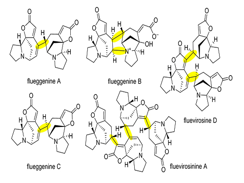 Total Synthesis of Flueggenine C via an Accelerated Intermolecular Rauhut-Currier Reaction
The first total synthesis of dimeric securinega alkaloid (-)-flueggenine C was completed via an accelerated intermolecular Rauhut–Currier (RC) reaction. The research team led by Professor Sunkyu Han in the Department of Chemistry succeeded in synthesizing the natural product by reinventing the conventional RC reaction.
The total synthesis of natural products refers to the process of synthesizing secondary metabolites isolated from living organisms in the laboratory through a series of chemical reactions. Each stage of chemical reaction needs to be successful to produce the final target molecule, and thus the process requires high levels of patience and creativity. For that reason, the researchers working on natural products total synthesis are often called “molecular artists”.
Despite numerous reports on the total synthesis of monomeric securinegas, the synthesis of dimeric securinegas, whose monomeric units are connected by a putative enzymatic RC reaction, has not been reported to date.
The team used a Rauhut-Currier (RC) reaction, a carboncarbon bond forming a reaction between two Michael acceptors first reported by Rauhut and Currier in 1963, to successfully synthesize a dimeric natural product, flueggenine C. This new work featured the first application of an intermolecular RC reaction in total synthesis.
The conventional intermolecular RC reaction was driven non-selectively by a toxic nucleophilic catalyst at a high temperature of over 150°C and a highly concentrated reaction mixture, and thus has never been applied to natural products total synthesis. To overcome this long-standing problem, the research team placed a nucleophilic moiety at the γ-position of the enone derivative. As a result, the RC reaction could be induced by the simple addition of a base at ambient temperature and dilute solution, without the need of a nucleophilic catalyst. Using this newly discovered reactivity, the team successfully synthesized the natural product (-)-flueggenine C from commercially available amino acid derivative in 12 steps.
Professor Han said, “Our key finding regarding the remarkably improved reactivity and selectivity of the intermolecular RC reaction will serve as a significant stepping stone in allowing this reaction to be considered a practical and reliable chemical tool with broad applicability in natural products, pharmaceuticals, and materials syntheses. ”
This research was led by Ph.D. candidate Sangbin Jeon and was published in The Journal of the American Chemical Society (JACS) on May 10. This research was funded by KAIST start-up funds, HRHR (High-Risk High-Return), RED&B (Research, Education, Development & Business) projects, the National Research Foundation of Korea, and the Institute for Basic Science.
(Figure 1: Representative dimeric/oligomeric securinega alkaloids)
(Figure 2: Our reinvented Rauhut-Currier reaction)
(Figure 3: Total Synthesis of (-)-flueggenine C)
2017.05.23 View 10460
 -
 Gout Diagnostic Strip Using a Single Teardrop
A novel diagnostic strip for gout patients using a single teardrop has been announced by KAIST research team. This technology analyzes biological molecules in tears for a non-invasive diagnosis, significantly reducing the time and expense previously required for a diagnosis.
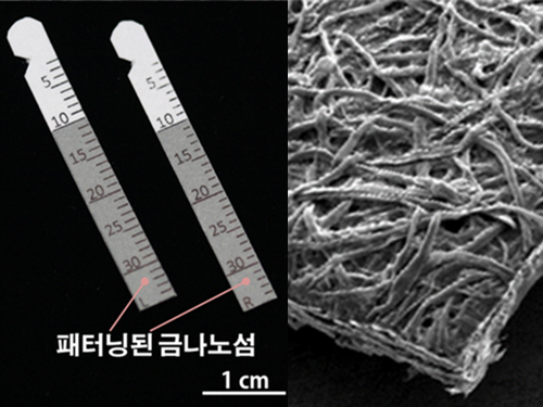
The research team under Professor Ki-Hun Jeong of the Department of Bio and Brain Engineering succeeded in developing an affordable and elaborate gout diagnostic strip by depositing metal nanoparticles on paper. This technology can not only be used in diagnostic medicine and drug testing, but also in various other areas such as field diagnoses that require prompt and accurate detection of a certain substance.
Gout induces pain in joints due to needle-shaped uric acid crystal build up. In general, therapeutic treatments exist to administer pain relief, stimulate uric acid discharge, and uric acid depressant. Such treatments work for temporary relief, but there have significant limitations. Thus, patients are required to regularly check uric acid concentrations, as well as control their diets. Therefore, simpler ways to measure uric acid would greatly benefit gout control and its prevention in a more affordable and convenient manner.
Existing gout diagnostic techniques include measuring uric acid concentrations from blood samples or observing uric acid crystals from joint synovial fluid under a microscope. These existing methods are invasive and time consuming. To overcome their limitations, the research team uniformly deposited gold nanoislands with nanoplasnomics properties on the surface of paper that can easily collect tears.
Nanoplasnomics techniques collect light on the surface of a metal nanostructure, and can be applied to disease and health diagnostic indicators as well as for genetic material detection. Further, metals such as gold absorb stronger light when it is irradiated, and thus can maximize light concentration on board surfaces while maintaining the properties of paper. The developed metal nanostructure production technology allows the flexible manufacturing of nanostructures on a large surface, which in turn allows flexible control of light concentrations.
The research team grafted surface-enhanced Raman spectroscopy on paper diagnostic strips to allow uric acid concentration measurements in teardrops without additional indicators. The measured concentration in teardrops can be compared to blood uric acid concentrations for diagnosing gout.
Professor Jeong explained, “Based on these research results, our strip will make it possible to conduct low-cost, no indicator, supersensitive biological molecule analysis and fast field diagnosis using tears.” He continued, “Tears, as well as various other bodily fluids, can be used to contribute to disease diagnosis and physiological functional research.”
Ph.D. candidate Moonseong Park participated in the research as the first author of the paper that was published in the online edition of ACS Nano on December 14, 2016. Park said, “The strip will allow fast and simple field diagnosis, and can be produced on a large scale using the existing semiconductor process.”
(Figure 1. Optical image of paper gout diagnostic strip covered with gold)
(Figure 2. Scanning delectron microscopic image of paper gout diagnostic strip)
(Figure 3. Scanning electron microscope image of cellulos fiber coated with gold nanoislands)
(Figure 4. Gout diagnosis using tears)
2017.04.27 View 9628
 -
 Professor Lee Recognized by the KMS as Best Paper Awardee
Professor Ji Oon Lee of the Department of Mathematical Sciences was selected as the 2017 Best Paper Awardee by the Korean Mathematical Society. The award will be presented during the KMS spring meeting on April 29. Dr. Lee is being honored for proving a necessary and sufficient condition for the Tracy-Wisdom law of Wigner matrices. In a paper titled ‘A Necessary and Sufficient Condition for Edge Universality of Wigner Matrices,’ he proposed a solution for one of the many unanswered problems in the field of random matrix theory that have existed for decades. The paper, co-authored with Professor Jun Yin at the University of Wisconsin – Madison, was published in the Duke Mathematical Journal in 2014. Professor Lee joined KAIST in 2010 after finishing his Ph.D. at Harvard University. He was named a ‘POSCI Science Fellow’ and received the ‘Young Scientist Award’ from the KMS in 2014.
2017.04.27 View 10887
 -
 Nuclease-Resistant Hybrid Nanoflowers
An eco-friendly method to synthesize DNA-copper nanoflowers with high load efficiencies, low cytotoxicity, and strong resistance against nucleases has been developed by Professor Hyun Gyu Park in the Department of Chemical and Biomolecular Engineering and his collaborators.
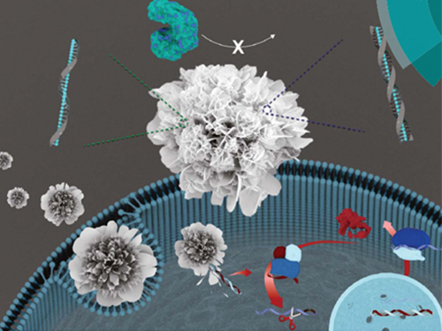
The research team successfully formed a flower-shaped nanostructure in an eco-friendly condition by using interactions between copper ions and DNA containing amide and amine groups. The resulting nanoflowers exhibit high DNA loading capacities in addition to low cytotoxicity.
Flower-shaped nanocrystals called nanoflowers have gained attention for their distinct features of high surface roughness and high surface area to volume ratios. The nanoflowers have been used in many areas including catalysis, electronics, and analytical chemistry.
Of late, research breakthroughs were made in the generation of hybrid inorganic-organic nanoflowers containing various enzymes as organic components. The hybridization with inorganic materials greatly enhanced enzymatic activity, stability, and durability compared to the corresponding free enzymes.
Generally, the formation of protein nanocrystals requires high heat treatment so it has limitations for achieving the high loading capacities of intact DNA.
The research team addressed the issue, focusing on the fact that nucleic acids with well-defined structures and selective recognition properties also contain amide and amine groups in their nucleobases. They proved that flower-like structures could be formed by using nucleic acids as a synthetic template, which paved the way to synthesize the hybrid nanoflowers containing DNA as an organic component in an eco-friendly condition.
The team also confirmed that this synthetic method can be universally applied to any DNA sequences containing amide and amine groups. They said their approach is quite unique considering that the majority of previous works focused on the utilization of DNA as a linker to assemble the nanomaterials. They said the method has several advantageous features. First, the ‘green’ synthetic procedure doesn’t involve any toxic chemicals, and shows low cytotoxicity and strong resistance against nucleases. Second, the obtained nanoflowers exhibit exceptionally high DNA loading capacities.
Above all, such superior features of hybrid nanoflowers enabled the sensitive detection of various molecules including phenol, hydrogen peroxide, and glucose. DNA-copper nanoflowers showed even higher peroxidase activity than those of protein-copper nanoflowers, which may be due to the larger surface area of the flower- shaped structures, creating a greater chance for applying them in the field of sensing of detection of hydrogen peroxide.
The research team expects that their research will create diverse applications in many areas including biosensors and will be further applied into therapeutic applications.
Professor Park said, “The inorganic component in the hybrid nanoflowers not only exhibits low cytotoxicity, but also protects the encapsulated DNA from being cleaved by endonuclease enzymes. Using this feature, the nanostructure will be applied into developing gene therapeutic carriers.”
This research was co-led by Professor Moon Il Kim at Gachon University and KAIST graduate Ki Soo Park, currently a professor at Konkuk University, is the first author. The research was featured as the front cover article of the Journal of Materials Chemistry B on March 28, Issue 12, published by the Royal Society of Chemistry.
The research was funded by the Mid-Career Researcher Support Program of the National Research Foundation of Korea and the Global Frontier Project of the Ministry of Science, ICT & Future Planning.
(Figure: (A) Schematic illustration of the formation of nuclease-resistant DNA–inorganic nanoflowers. (B) SEM images showing time-dependent growth of DNA-nanoflowers. The concentration of A-rich ssDNA (Table S1, ESI†) was 0.25 mM.)
2017.04.14 View 10020
 -
 A Transport Technology for Nanowires Thermally Treated at 700 Celsius Degrees
Professor Jun-Bo Yoon and his research team of the Department of Electrical Engineering at KAIST developed a technology for transporting thermally treated nanowires to a flexible substrate and created a high performance device for collecting flexible energy by using the new technology.
Mr. Min-Ho Seo, a Ph.D. candidate, participated in this study as the first author. The results were published online on January 30th in ACS Nano, an international journal in the field of nanoscience and engineering. (“Versatile Transfer of an Ultralong and Seamless Nanowire Array Crystallized at High Temperature for Use in High-performance Flexible Devices,” DOI: 10.1021/acsnano.6b06842)
Nanowires are one of the most representative nanomaterials. They have wire structures with dimensions in nanometers. The nanowires are widely used in the scientific and engineering fields due to their prominent physical and chemical properties that depend on a one-dimensional structure, and their high applicability.
Nanowires have much higher performance if their structure has unique features such as an excellent arrangement and a longer-than-average length. Many researchers are thus actively participating in the research for making nanowires without much difficulty, analyzing them, and developing them for high performance application devices.
Scientists have recently favored a research topic on making nanowires chemically and physically on a flexible substrate and applies the nanowires to a flexible electric device such as a high performance wearable sensor.
The existing technology, however, mixed nanowires from a chemical synthesis with a solution and spread the mixture on a flexible substrate. The resultant distribution was random, and it was difficult to produce a high performance device based on the structural advantages of nanowires. In addition, the technology used a cutting edge nano-process and flexible materials, but this was not economically beneficial. The production of stable materials at a temperature of 700 Celsius degrees or higher is unattainable, a great challenge for the application.
To solve this problem, the research team developed a new nano-transfer technology that combines a silicon nano-grating board with a large surface area and a nano-sacrificial layer process. A nano-sacrificial layer exists between nanowires and a nano-grating board, which acts as the mold for the nano-transfer. The new technology allows the device undergo thermal treatment. After this, the layer disappears when the nanowires are transported to a flexible substrate.
This technology also permits the stable production of nanowires with secured properties at an extremely high temperature. In this case, the nanowires are neatly organized on a flexible substrate. The research team used the technology to manufacture barium carbonate nanowires on top of the flexible substrate. The wires secured their properties at a temperature of 700℃ or above. The team employed the collection of wearable energy to obtain much higher electrical energy than that of an energy collecting device designed based on regular barium titanate nanowires.
The researchers said that their technology is built upon a semiconductor process, known as Physical Vapor Deposition that allows various materials such as ceramics and semiconductors to be used for flexible substrates of nanowires. They expected that high performance flexible electric devices such as flexible transistors and thermoelectric elements can be produced with this method.
Mr. Seo said, “In this study, we transported nanowire materials with developed properties on a flexible substrate and showed an increase in device performance. Our technology will be fundamental to the production of various nanowires on a flexible substrate as well as the feasibility of making high performance wearable electric devices.”
This research was supported by the Leap Research Support Program of the National Research Foundation of Korea.
Fig. 1. Transcription process of new, developed nanowires (a) and a fundamental mimetic diagram of a nano-sacrificial layer (b)
Fig. 2. Transcription results from using gold (AU) nanowires. The categories of the results were (a) optical images, (b) physical signals, (c) cross-sectional images from a scanning electron microscope (SEM), and (d-f) an electric verification of whether the perfectly arranged nanowires were made on a large surface.
Fig. 3. Transcription from using barium titanate (BaTiO3) nanowires. The results were (a) optical images, (b-e) top images taken from an SEM in various locations, and (f, g) property analysis.
Fig. 4. Mimetic diagram of the energy collecting device from using a BaTiO3 nanowire substrate and an optical image of the experiment for the miniature energy collecting device attached to an index finger.
2017.03.22 View 10269
 -
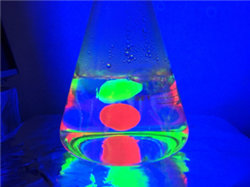 Quantum Dot Film Can Withstand High Temperatures and Humidity
The joint KAIST research team of Professor Byeong-Soo Bae of the Department of Materials Science and Engineering and Professor Doh Chang Lee of the Department of Chemical and Biomolecular Engineering was able to fabricate a siloxane-encapsulated quantum dot film, which exhibits stable emission intensity over one month even at high temperatures and humidity.
The results of this study were published in the Journal of the American Chemical Society (JACS) on November 29, 2016. The research article is entitled “Quantum Dot/Siloxane Composite Film Exceptionally Stable against Oxidation under Heat and Moisture.” (DOI: 10.1021/jacs.6b10681)
Quantum dots (QDs), light-emitting diodes (LEDs) for next-generation displays, are tiny particles or nanocrystals of semiconducting materials. Their emission wavelength can easily be adjusted by changing their sizes, which are just a few nanometers. A wide spectrum of their colors can also achieve ultra-high definition displays.
Due to these characteristics, QDs are coated on a film as a polymer resin in dispersed form, or they are spread on an LED light source. They are thus considered to be crucial for next generation displays.
Despite their exceptional optical properties, however, QDs are easily oxidized in a high temperature and high humidity environment, and, as a result, this greatly deteriorates their luminescence quality (quantum efficiency). Therefore, they are encapsulated in an extra thin layer to block oxygen and moisture.
QD displays in the current market have a film inserted to separate them from LEDs, which create heat. The high unit cost of this protective layer, however, increases the overall cost of displays, lowering their price competitiveness in the market.
For a solution, the research team applied the sol-gel condensation reaction of silane precursors with QDs. This technology uses the reactions of chemical substances to synthesize ceramics or glass at a low temperature.
The team applied QDs in a heat resistant siloxane polymer by employing this technology. The siloxane resin acted as a cup holding the QDs and also blocked heat and moisture. Thus, their performance can be maintained without an extra protective film.
QDs are evenly dispersed into the resin from a chemical process to fabricate a QD embedded film and retained the high quality luminescence not only at a high temperature of 85°C and in a high humidity of 85%, but also in a high acid and high base environment. Remarkably though, the luminescence actually increased in the high humidity environment.
If this technology is used, the overall price of displays will decrease by producing a stable QD film without an extra protective barrier. In the future, the QD film can be directly applied to a blue LED light source. As a result, it will be possible to develop a QD display that can reduce the amount of QDs needed and improve its performance.
Professor Bae said, “We have proposed a way to make quantum dots overcome their limitations and have wide applications as they are being developed for next-generation displays. Our technology will make significant contributions to the display industry in the country.”
He also added, “In the future, we plan to cooperate with companies both in and out of the country to improve the performance of quantum dots and concentrate on their commercialization.”
The research team is currently applying for related patents both in and out of the country. The team is also plan ning to transfer the patents to Sol Ip Technology Inc., a company founded at KAIST, to start the commercialization.
Picture 1:
Siloxane-encapsulated quantum dot (QD) films showing performance stability in boiling water
Picture 2 and 3:
So-gel condensation reaction in silane precursors between Methacryloxypropyltrimethoxysilane (MPTS) and diphenylsilanediol (DPSD). The inset shows photographs of a QD-oligosiloxane resin under room light (left) and a UV lamp (λ = 365 nm) (right).
Free radical addition reactions among carbon double bonds of methacryl functional groups and oleic acids. The inset shows photographs of a QD-silox film under room light (left) and a UV lamp (λ = 365 nm) (right).
2017.02.24 View 11104
 -
 An Improved Carbon Nanotube Semiconductor
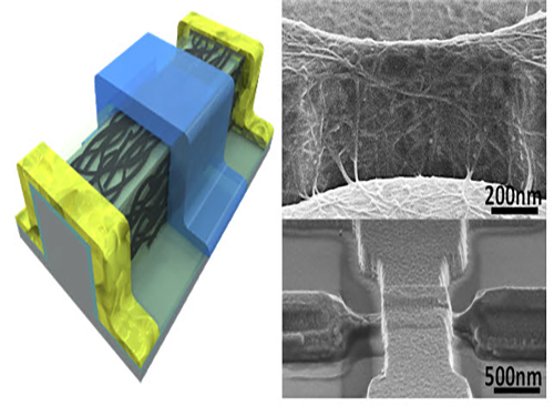
Professor Yang-Kyu Choi and his research team of the School of Electrical Engineering at KAIST collaborated with Professor Sung-Jin Choi of Kookmin University to develop a large-scale carbon nanotube semiconductor by using a 3-D fin-gate structure with carbon nanotubes on its top.
Dong Il Lee, a postdoctoral researcher at KAIST’s Electrical Engineering School, participated in this study as the first author. It was published in ACS Nano on November 10, 2016, and was entitled “Three-Dimensional Fin-Structured Semiconducting Carbon Nanotube Network Transistor.”
A semiconductor made with carbon nanotubes operates faster than a silicon semiconductor and requires less energy, yielding higher performance.
Most electronic equipment and devices, however, use silicon semiconductors because it is difficult to fabricate highly purified and densely packed semiconductors with carbon nanotubes (CNTs).
To date, the performance of CNTs was limited due to their low density. Their purity was also low, so it was impossible to make products that had a constant yield on a large-surface wafer or substrate. These characteristics made the mass production of semiconducting CNTs difficult.
To solve these difficulties, the research team used a 3-D fin-gate to vapor-deposit carbon nanotubes on its top. They developed a semiconductor that had a high current density with a width less than 50 nm.
The three-dimensional fin structure was able to vapor-deposit 600 carbon nanotubes per micrometer. This structure could have 20 times more nanotubes than the two dimensional structure, which could only vapor-deposit thirty in the same 1 micrometer width.
In addition, the research team used semi-conductive carbon nanotubes having a purity rating higher than 99.9% from a previous study to obtain a high yield semiconductor.
The semiconductor from the research group has a high current density even with a width less than 50 μm. The new semiconductor is expected to be five times faster than a silicon-based semiconductor and will require five times less electricity during operation.
Furthermore, the new semiconductor can be made by or will be compatible with the equipment for producing silicon-based semiconductors, so there will be no additional costs.
Researcher Lee said, “As a next generation semiconductor, the carbon nanotube semiconductor will have better performance, and its effectiveness will be higher.” He also added, “Hopefully, the new semiconductor will replace the silicon-based semiconductors in ten years.”
This study received support from the Center for Integrated Smart Sensors funded by the Ministry of Science, ICT & Future Planning of Korea as the Global Frontier Project, and from the CMOS (Complementary Metal-Oxide-Semiconductor) THz Technology Convergence Center of the Pioneer Research Center Program sponsored by the National Research Foundation of Korea.
Picture 1: 3D Diagram of the Carbon Nanotube Electronic Device and Its Scanning Electron Microscope (SEM) Image
Picture 2: 3D Transistor Device on an 8-inch Base and the SEM Image of Its Cross Section
2017.02.16 View 12228
 -
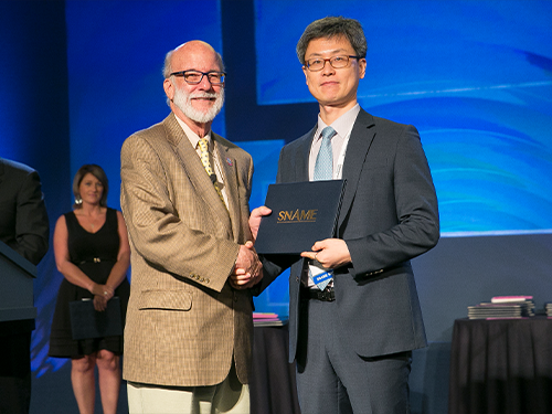 Professor Hyun Chung Claims the Elmer L. Hann Award 2016
Professor Hyun Chung of KAIST’s Mechanical Engineering Department received the Elmer L. Hann Award 2016 at the SNAME Maritime Convention (SMC) that took place November 1-5 in Seattle, Washington, in the United States.
Held annually, the SMC is the largest academic gathering for researchers and professionals in maritime and ocean engineering, and it is hosted by the Society of Naval Architects and Marine Engineers (SNAME).
With more than 6,000 members around the world in 85 countries, SNAME is an internationally-recognized, non-profit, professional society of individual members serving the maritime and offshore industries and their suppliers. It strives to advance the art, science, and practice of naval architecture, marine engineering, ocean engineering, and other marine-related professions through the exchange of knowledge and ideas, as well as the promotion of R&D, and education.
Every year, SNAME selects three research papers that are either published in its academic journal or presented at its sponsored conferences and awards them, respectively. One of the three awards is the Elmer L. Hann Award.
This year, the Society announced Professor Chung’s paper as the Elmer L. Hann Award winner. His paper, entitled “Tolerance Analysis and Diagnosis Model of Compliant Block Assembly Considering Welding Deformation,” was presented at the World Maritime Technology Conference held November 3-7, 2015 in Providence, Rhode Island, USA.
Analysis, management, and diagnostics of tolerance are important factors in the production of ocean structures. In the paper, Professor Chung’s team proposed a simplified tolerance analysis and diagnosis model including the effects of welding distortion for accuracy control in ship block assembly, thereby improving the production process.
Professor Chung said, “This is indeed a wonderful award for our team. From early this year, with support from the U.S. Office of Naval Research, we have collaborated with the University of Michigan, the Massachusetts Institute of Technology, Ohio State University, and the Edison Welding Institute to study this topic more deeply. We will keep up the good work to make meaningful progress.”
2016.12.10 View 9297
 -
 Professor Kwon to Represent the Asia-Pacific Region of the IEEE RAS
Professor Dong-Soon Kwon of the Mechanical Engineering Department at KAIST has been reappointed to the Administrative Committee of the Institute of Electrical and Electronics Engineers (IEEE) Robotics and Automation Society (IEEE RAS). Beginning January 1, 2017, he will serve his second three-year term, which will end in 2019. In 2014, he was the first Korean appointed to the committee, representing the Asia-Pacific community of the IEEE Society.
Professor Kwon said, “I feel thankful but, at the same time, it is a great responsibility to serve the Asian research community within the Society. I hope I can contribute to the development of robotics engineering in the region and in Korea as well.”
Consisted of 18 elected members, the administrative committee manages the major activities of IEEE RAS including hosting its annual flagship meeting, the International Conference on Robotics and Automation.
The IEEE RAS fosters the advancement in the theory and practice of robotics and automation engineering and facilitates the exchange of scientific and technological knowledge that supports the maintenance of high professional standards among its members.
2016.12.06 View 11529
 -
 KAIST's Doctoral Student Receives a Hoffman Scholarship Award
Hyo-Sun Lee, a doctoral student at the Graduate School of EEWS (Environment, Energy, Water and Sustainability), KAIST, is a recipient of the 2016 Dorothy M. and Earl S. Hoffman Scholarships presented by the American Vacuum Society (AVS). The award ceremony took place during the Society’s 63rd International Symposium and Exhibition on November 6-11, 2016 in Nashville, Tennessee.
Lee is the first Korean and foreign student to receive this scholarship.
The Hoffman Scholarships were established in 2002 to recognize and encourage excellence in graduate studies in the sciences and technologies of interest to AVS. The scholarships are funded by a bequest from Dorothy M. Hoffman, who was a pioneering member of the Society of Women Engineers and served as the president of AVS in 1974.
Lee received the scholarship for her research that detects hot electrons from chemical reactions on catalytic surface using nanodevices. Nano Letters, an academic journal published by the American Chemical Society, described her work in its February 2016 issue as a technology that allows quantitative analysis of hot electrons by employing a new nanodevice and therefore helps researchers understand better the mechanism of chemical reactions on nanocatalytic surface. She also published her work to detect the flow of hot electrons that occur on metal nanocatalytic surface during hydrogen oxidation reactions in Angewandte Chemie.
Lee said, “I am pleased to receive this honor from such a world-renowned academic society. Certainly, this will be a great support for my future study and research.”
Founded in 1953, AVS is an interdisciplinary, professional society composed of approximately 4,500 members worldwide. It supports networking among academic, industrial, government, and consulting professionals involved in a range of established and emerging science and technology areas such as chemistry, physics, engineering, business, and technology development.
2016.11.17 View 11188
 -
 Extremely Thin and Highly Flexible Graphene-Based Thermoacoustic Speakers
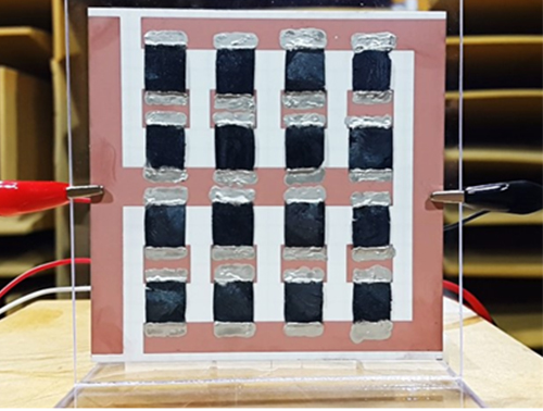
A joint research team led by Professors Jung-Woo Choi and Byung Jin Cho of the School of Electrical Engineering and Professor Sang Ouk Kim of the Material Science and Engineering Department, all on the faculty of the Korea Advanced Institute of Science and Technology (KAIST), has developed a simpler way to mass-produce ultra-thin graphene thermosacoustic speakers.
Their research results were published online on August 17, 2016 in a journal called Applied Materials & Interfaces. The IEEE Spectrum, a monthly magazine published by the Institute of Electrical and Electronics Engineers, reported on the research on September 9, 2016, in an article titled, “Graphene Enables Flat Speakers for Mobile Audio Systems.” The American Chemical Society also drew attention to the team’s work in its article dated September 7, 2016, “Bringing Graphene Speakers to the Mobile Market.”
Thermoacoustic speakers generate sound waves from temperature fluctuations by rapidly heating and cooling conducting materials. Unlike conventional voice-coil speakers, thermoacoustic speakers do not rely on vibrations to produce sound, and thus do not need bulky acoustic boxes to keep complicated mechanical parts for sound production. They also generate good quality sound in all directions, enabling them to be placed on any surface including curved ones without canceling out sounds generated from opposite sides.
Based on a two-step, template-free fabrication method that involved freeze-drying a solution of graphene oxide flakes and the reduction/doping of oxidized graphene to improve electrical properties, the research team produced a N-doped, three-dimensional (3D), reduced graphene oxide aerogel (N-rGOA) with a porous macroscopic structure that permitted easy modulation for many potential applications.
Using 3D graphene aerogels, the team succeeded in fabricating an array of loudspeakers that were able to withstand over 40 W input power and that showed excellent sound pressure level (SPL), comparable to those of previously reported 2D and 3D graphene loudspeakers.
Choong Sun Kim, the lead author of the research paper and a doctoral student in the School of Electrical Engineering at KAIST, said:
“Thermoacoustic speakers have a higher efficiency when conducting materials have a smaller heat capacity. Nanomaterials such as graphene are an ideal candidate for conductors, but they require a substrate to support their extremely thinness. The substrate’s tendency to lose heat lowers the speakers’ efficiency. Here, we developed 3D graphene aerogels without a substrate by using a simple two-step process. With graphene aerogels, we have fabricated an array of loudspeakers that demonstrated stable performance. This is a practical technology that will enable mass-production of thermosacoustic speakers including on mobile platforms.”
The research paper is entitled “Application of N-Doped Three-Dimensional Reduced Graphene Oxide Aerogel to Thin Film Loudspeaker.” (DOI: 10.1021/acsami.6b03618)
Figure 1: A Thermoacoustic Loudspeaker Consisted of an Array of 16 3D Graphene Aerogels
Figure 2: Two-step Fabrication Process of 3D Reduced Graphene Oxide Aerogel Using Freeze-Drying and Reduction/Doping
Figure 3: X-ray Photoelectron Spectroscopy Graph of the 3D Reduced Graphene Oxide Aerogel and Its Scanning Electron Microscope Image
2016.10.05 View 15351
 -
 Continuous Roll-Process Technology for Transferring and Packaging Flexible Large-Scale Integrated Circuits
A research team led by Professor Keon Jae Lee from KAIST and by Dr. Jae-Hyun Kim from the Korea Institute of Machinery and Materials (KIMM) has jointly developed a continuous roll-processing technology that transfers and packages flexible large-scale integrated circuits (LSI), the key element in constructing the computer’s brain such as CPU, on plastics to realize flexible electronics.
Professor Lee previously demonstrated the silicon-based flexible LSIs using 0.18 CMOS (complementary metal-oxide semiconductor) process in 2013 (ACS Nano, “In Vivo Silicon-based Flexible Radio Frequency Integrated Circuits Monolithically Encapsulated with Biocompatible Liquid Crystal Polymers”) and presented the work in an invited talk of 2015 International Electron Device Meeting (IEDM), the world’s premier semiconductor forum.
Highly productive roll-processing is considered a core technology for accelerating the commercialization of wearable computers using flexible LSI. However, realizing it has been a difficult challenge not only from the roll-based manufacturing perspective but also for creating roll-based packaging for the interconnection of flexible LSI with flexible displays, batteries, and other peripheral devices.
To overcome these challenges, the research team started fabricating NAND flash memories on a silicon wafer using conventional semiconductor processes, and then removed a sacrificial wafer leaving a top hundreds-nanometer-thick circuit layer. Next, they simultaneously transferred and interconnected the ultrathin device on a flexible substrate through the continuous roll-packaging technology using anisotropic conductive film (ACF). The final silicon-based flexible NAND memory successfully demonstrated stable memory operations and interconnections even under severe bending conditions. This roll-based flexible LSI technology can be potentially utilized to produce flexible application processors (AP), high-density memories, and high-speed communication devices for mass manufacture.
Professor Lee said, “Highly productive roll-process was successfully applied to flexible LSIs to continuously transfer and interconnect them onto plastics. For example, we have confirmed the reliable operation of our flexible NAND memory at the circuit level by programming and reading letters in ASCII codes. Out results may open up new opportunities to integrate silicon-based flexible LSIs on plastics with the ACF packing for roll-based manufacturing.”
Dr. Kim added, “We employed the roll-to-plate ACF packaging, which showed outstanding bonding capability for continuous roll-based transfer and excellent flexibility of interconnecting core and peripheral devices. This can be a key process to the new era of flexible computers combining the already developed flexible displays and batteries.”
The team’s results will be published on the front cover of Advanced Materials (August 31, 2016) in an article entitled “Simultaneous Roll Transfer and Interconnection of Silicon NAND Flash Memory.” (DOI: 10.1002/adma.201602339)
YouTube Link: https://www.youtube.com/watch?v=8OJjAEm27sw
Picture 1: This schematic image shows the flexible silicon NAND flash memory produced by the simultaneous roll-transfer and interconnection process.
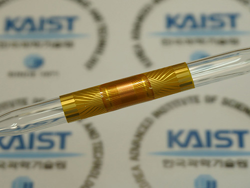
Picture 2: The flexible silicon NAND flash memory is attached to a 7 mm diameter glass rod.
2016.09.01 View 12736