Engineering
-
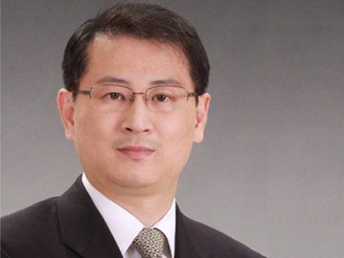 Professor Keon-Jae Lee Lectures at IEDM and ISSCC Forums
Professor Keon-Jae Lee of KAIST’s Materials Science and Engineering Department delivered a speech at the 2015 Institute of Electrical and Electronics Engineers (IEEE) International Electron Devices Meeting (IEDM) held on December 7-9, 2015 in Washington, D.C.
He will also present a speech at the 2016 International Solid-State Circuits Conference scheduled on January 31-February 4, 2016 in San Francisco, California.
Both professional gatherings are considered the world’s most renowned forums in electronic devices and semiconductor technology. It is rare for a Korean researcher to be invited to speak at these global conferences.
Professor Lee was recognized for his research on flexible NAND chips. The Korea Times, an English language daily newspaper in Korea, reported on his participation in the forums and his recent work. An excerpt of the article follows below:
“KAIST Professor to Lecture at Renowned Tech Forums”
By Lee Min-hyung, The Korea Times, November 26, 2015
Recently he has focused on delivering technologies for producing flexible materials that can be applied to everyday life. The flexible NAND flash memory chips are expected to be widely used for developing flexible handsets. His latest research also includes flexible light-emitting diodes (LED) for implantable biomedical applications.
Lee is currently running a special laboratory focused on developing new flexible nano-materials. The research group is working to develop what it calls “self-powered flexible electronic systems” using nanomaterials and electronic technology.
Lee’s achievement with flexible NAND chips was published in the October edition of Nano Letters, the renowned U.S.-based scientific journal.
He said that flexible memory chips will be used to develop wearable computers that can be installed anywhere.
2015.11.26 View 13432
 -
 A KAIST Student Donates USD 26,000 to His Alma Mater
A KAIST undergraduate student who developed and sold a smart phone application donated USD 26,000 to his alma mater.
Seung-Kyu Oh of the School of Electrical Engineering gave his donation to President Steve Kang of KAIST on November 24, 2015. This is the largest amount donated by an enrolled undergraduate.
In 2010, at a time when android smart phones were just being released, Mr. Oh decided to develop a subway app because existing subway apps were not user-friendly.
Mr. Oh’s “Subway Navigation” app checks the current operation hours and gives users the shortest path when the user selects points of departure and arrival. The calculation for the shortest path involves factors such as which train comes first, where and to what train to transfer, the first and last trains of the day, transfer passageway usage time, etc.
To make the app useful to the largest number of people, Mr. Oh distributed it on the open market. Currently, the app is ranked the second most downloaded subway app, and has even made considerable advertising profits, having accumulated more than 5,000,000 users. This year, Mr. Oh received an offer from Kakao, an Internet company based in Seoul, Korea, to take over the app and sold it to them.
Mr. Oh said that making a donation KAIST was the first thing that came to his mind when he earned this profit.
Mr. Oh, who graduated from the Korea Science Academy, a science magnet high school, said that he felt a sense of responsibility for receiving support from Korea since high school, and that he decided to donate to KAIST as a way of returning the support that he had received so far.
He further said that “if an individual’s efforts and talents created some profit together with what he or she learned from school, then the school that supported the student in furthering his studies has also played a significant role,” and that “likewise, our stellar alumni can contribute more to our younger classmates’ growth and development.”
Mr. Oh, who is at his last semester, plans to join Kakao and will take on a job managing his subway app.
President Kang said he hopes that “all KAISTians will emulate Mr. Oh’s example to support the school” and that “the university will use the money to invest further in its future.”
2015.11.24 View 5008
 -
 HUBO to Present at the 2016 World Economic Forum
KAIST researchers will lead an IdeasLab on biotechnology for an aging society while HUBO, the winner of the 2015 DARPA Robotics Challenge, will interact with the forum participants, offering an experience of state-of-the-art robotics technology.
Representatives from KAIST will attend the 2016 Annual Meeting of the World Economic Forum to run an IdeasLab and showcase its humanoid robot.
With over 2,500 leaders from business, government, international organizations, civil society, academia, media, and the arts expected to participate, the 2016 Annual Meeting will take place on January 20-23, 2016 in Davos-Klosters, Switzerland. Under the theme of “Mastering the Fourth Industrial Revolution,” global leaders will discuss the period of digital transformation that will have profound effects on economies, societies, and human behavior.
President Sung-Mo Kang will join the Global University Leaders Forum (GULF), a high-level academic meeting to foster collaboration among experts on issues of global concern for the future of higher education and the role of science in society. He will discuss how the emerging revolution in technology will affect the way universities operate and serve society. KAIST is the only Korean university participating in GULF, which is composed of prestigious universities invited from around the world.
Four KAIST professors, including Distinguished Professor Sang Yup Lee of the Chemical and Biomolecular Engineering Department, will lead an IdeasLab on “Biotechnology for an Aging Society.”
Professor Lee said, “In recent decades, much attention has been paid to the potential effect of the growth of an aging population and problems posed by it. At our IdeasLab, we will introduce some of our research breakthroughs in biotechnology to address the challenges of an aging society.”
In particular, he will present his latest research in systems biotechnology and metabolic engineering. His research has explained the mechanisms of how traditional Oriental medicine works in our bodies by identifying structural similarities between effective compounds in traditional medicine and human metabolites, and has proposed more effective treatments by employing such compounds.
KAIST will also display its networked mobile medical service system, “Dr. M.” Built upon a ubiquitous and mobile Internet, such as the Internet of Things, wearable electronics, and smart homes and vehicles, Dr. M will provide patients with a more affordable and accessible healthcare service.
In addition, Professor Jun-Ho Oh of the Mechanical Engineering Department will showcase his humanoid robot, “HUBO,” during the Annual Meeting. His research team won the International Humanoid Robotics Challenge hosted by the United States Defense Advanced Research Projects Agency (DARPA), which was held in Pomona, California, on June 5-6, 2015. With 24 international teams participating in the finals, HUBO completed all eight tasks in 44 minutes and 28 seconds, 6 minutes earlier than the runner-up, and almost 11 minutes earlier than the third-place team. Team KAIST walked away with the grand prize of USD 2 million.
Professor Oh said, “Robotics technology will grow exponentially in this century, becoming a real driving force to expedite the Fourth Industrial Revolution. I hope HUBO will offer an opportunity to learn about the current advances in robotics technology.”
President Kang pointed out, “KAIST has participated in the Annual Meeting of the World Economic Forum since 2011 and has engaged with a broad spectrum of global leaders through numerous presentations and demonstrations of our excellence in education and research. Next year, we will choreograph our first robotics exhibition on HUBO and present high-tech research results in biotechnology, which, I believe, epitomizes how science and technology breakthroughs in the Fourth Industrial Revolution will shape our future in an unprecedented way.”
2015.11.18 View 13841
 -
 A KAIST Alumnus Is Appointed the President of Seoul National University of Science and Technology
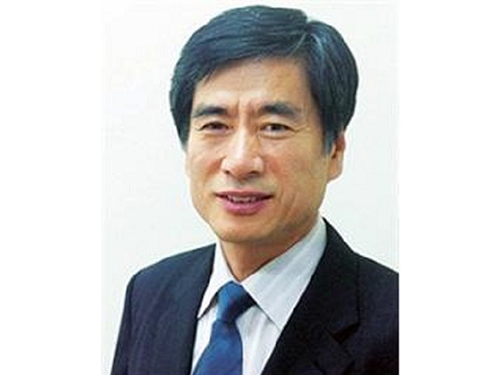
Jong-Ho Kim, graduated from the master’s program in the mechanical engineering department of KAIST in 1980, has been appointed the 11th president of Seoul National University of Science and Technology (SeoulTech) on November 9, 2015.
Upon receiving his doctoral degree in production engineering from KAIST in 1986, President Kim began his career as a professor at SeoulTech. He served in many senior posts at the university including Dean of Planning and Academic Affairs, and of the Engineering College.
2015.11.15 View 5424
 -
 Using Light to Treat Alzheimer's Disease
Medical application of photoactive chemicals offers a promising therapeutic strategy for neurodegenerative diseases.
A research team jointly led by Professor Chan Beum Park of the Materials Science and Engineering Department at KAIST and Dr. Kwon Yu from the Bionano Center at the Korea Research Institute of Bioscience and Biotechnology (KRIBB) conducted research to suppress an abnormal assembly of beta-amyloids, a protein commonly found in the brain, by using photo-excited porphyrins.
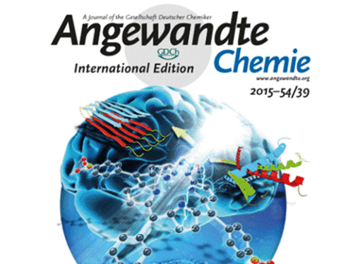
Beta-amyloid plaques are known to cause Alzheimer's disease. This research finding suggests new ways to treat neurodegenerative illnesses including Alzheimer's disease. It was published online as the lead article in the September 21th issue of Angewandte Chemie. The title of the article is “Photo-excited Porphyrins as a Strong Suppressor of ß-Amyloid Aggregation and Synaptic Toxicity.”
Light-induced treatments using organic photosensitizers have advantages to managing the treatment in time and area. In the case of cancer treatments, doctors use photodynamic therapies where a patient is injected with an organic photosensitizer, and a light is shed on the patient’s lesion. However, such therapies had never been employed to treat neurodegenerative diseases.
Alzheimer's starts when a protein called beta-amyloid is created and deposited in a patient’s brain. The abnormally folded protein created this way harms the brain cells by inducing the degradation of brain functions, for example, dementia. If beta-amyloid creation can be suppressed at an early stage, the formation of amyloid deposits will stop. This could prevent Alzheimer’s disease or halt its progress.
The research team effectively prevented the buildup of beta-amyloids by using blue LED lights and a porphyrin inducer, which is a biocompatible organic compound. By absorbing light energy, a photosensitizer such as porphyrin reaches the excitation state. Active oxygen is created as the porphyrin returns to its ground state. The active oxygen oxidizes a beta-amyloid monomer, and by combining with it, disturbs its assembly.
The technique was tested on drosophilae or fruit flies, which were produced to model Alzheimer on invertebrates. The research showed that symptoms of Alzheimer's disease in the fruit flies such as damage on synapse and muscle, neuronal apoptosis, degradation in motility, and decreased longevity were alleviated. Treatments with light provide additional benefits: less medication is needed than other drug treatments, and there are fewer side effects. When developed, photodynamic therapy will be used widely for this reason.
Professor Park said, “This work has significance as it was the first case to use light and photosensitizers to stop deposits of beta-amyloids. We plan to carry the research further by testing compatibility with other organic and inorganic photosensitizers and by changing the subject of photodynamic therapy to vertebrate such as mice.”
Picture 1 – Deposits of Beta-Amyloid in Fruit Flies Stopped by Using Porphyrin and Blue LED Lights
Picture 2 – The Research Finding Published as the Lead Article in Angewandte Chemie (September 2015)
2015.11.11 View 12080
 -
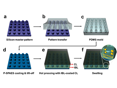 Membrane
Scientists at KAIST have developed a new way of making fuel cell membranes using nanoscale fasteners, paving the way for lower-cost, higher-efficiency and more easily manufactured fuel cells.
The internal workings of fuel cells vary, but basically all types mix hydrogen and oxygen to produce a chemical reaction that delivers usable electricity and exhausts ordinary water as a by-product. One of the most efficient types is the proton exchange membrane (PEM) fuel cell, which operates at low enough temperatures to be used in homes and vehicles.
To generate electricity, PEM fuel cells rely on two chemical compartments separated by a permeable catalyst membrane. This membrane acts as an electrolyte; a negative electrode is bonded to one side of the membrane and a positive electrode is bonded to the other. The electrolyte membrane is often based on a polymer of perfluorosulfonic acid. Due to its high cost, however, a less expensive hydrocarbon-based electrolyte membrane has attracted interest in this technology sector.
Until now, the challenge in adopting such a hydrocarbon membrane has been that the interface between the electrode and hydrocarbon membrane is weak. This causes the membrane to delaminate relatively easily, falling apart and losing efficiency with use.
Professor Hee-Tak Kim of the Department of Chemical and Biomolecular Engineering at the Korea Advanced Institute of Science and Technology (KAIST) and his research team have developed a new fastening system that bonds the two materials mechanically rather than chemically. This opens the way to the development of fuel cell membranes that are less expensive, easier to manufacture, stronger and more efficient.
The researchers achieved this by moulding a pattern of tiny cylindrical pillars on the face of the hydrocarbon membrane. The pillars protrude into a softened skin of the electrode with heat. The mechanical bond sets and strengthens as the material cools and absorbs water. The pillar-patterned hydrocarbon membrane is cast using silicone moulds.
Professor Kim said, “This physically fastened bond is almost five times stronger and harder to separate than current bonds between the same layers.”
The new interlocking method also appears to offer a way to bond many types of hydrocarbon membranes that, until now, have been rejected because they couldn’t be fastened robustly. This would make hydrocarbon membranes practical for a number of applications beyond fuel cells such as rechargeable “redox flow” batteries.
The research team is now developing a stronger and more scalable interlocking interface for their nanoscale fasteners.
Picture: Schematic Diagram of the Fabrication of the Pillar P-SPAES Membrane and Its Working Principle of Interlocking Effects
2015.11.06 View 10653
 -
 KAIST Hosts the Wearable Computer Contest 2015
“What you see is a compact electronic system on a dust mask, which monitors the amount of dust taken in by a worker and lets other workers know if the person is injured in an industrial site,” said Bum Taek Jung, a Master’s candidate from Sungkyunkwan University during the Wearable Computer Contest 2015 held in KI building of KAIST on November 5, 2015.
He explained his interest in developing this system, “Dust-related respiratory diseases and falling accidents are still prevalent in industrial sites.” He added, “Using the smart dust mask helps monitoring workers’ physical condition in real time, allowing us to cope with accidents in a much more timely manner.” A smart dust mask is a portable device that alerts the user with orange or red light signs when the amount of dust inhaled by the user is higher than the threshold. Its application on a smartphone can also allow project managers to alert the risk of falling accidents to workers by employing a gyroscope and an accelerometer on the mask.
The Wearable Computer Contest 2015 met for the eleventh time at KAIST on November 5-6, 2015. A wearable computer refers to a portable device which users can wear directly on the body or on their clothes while moving. Products that can provide various services by connecting to a smartphone have become increasingly popular. The contest is an excellent opportunity for university students to design creative wearable systems similar to those often depicted in movies and comics.
This year 102 teams from universities all over the nation participated. After screening and evaluation of their presentations, only 8 teams in the product section and 3 teams in the ideas section were selected for the finals. Of the many entries to the contest, the ECG security system caught many people’s attention. The wearable, which attaches to a shirt, acts like an electrocardiogram. By comparing the ECG reading with the one stored in the data server, the wearable can authenticate the user. The system could be widely used by enterprises and financial companies where tight security and authentication are crucial.
The winners of the product and the ideas sections received USD 4,300 and usd 860 respectively along with Minister Prizes from the Minister of Science, ICT and Future Planning of Korea. The Chairman of the contest, Professor Hoi-Jun Yoo from the Electrical Engineering Department of KAIST said, “The contest will be a great opportunity for anyone to have a look at advanced wearable devices developed through close integration of state-of-the-art technologies and creative ideas from young minds.”
2015.11.05 View 9508
 -
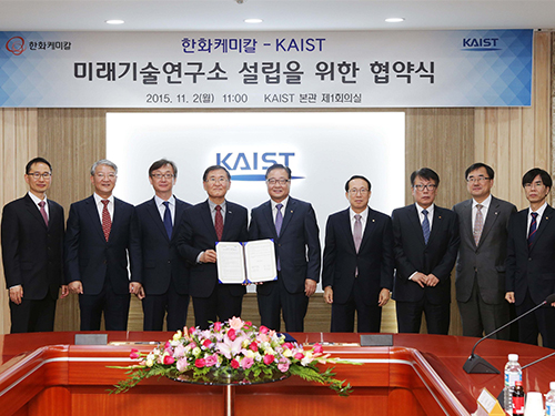 KAIST and Hanwha Chemical Agree on Research Collaboration
KAIST signed a memorandum of understanding (MOU) with Hanwha Chemical Co., Ltd., a Korean chemical and auto manufacturer, on November 2, 2015 to establish a research center on campus.
The research center, which will be named “KAIST-Hanwha Chemical Future Technology Research Center,” will implement joint research projects for five years beginning from 2016 to develop innovative, green technologies that will help the Korean chemical industry boost its global competitiveness and to nurture top researchers and engineers in chemical engineering.
The research center will lead the development of next-generation petrochemical materials and manufacturing technology and the establishment of pure high-refining processes which are more energy-efficient and environmentally friendly. KAIST and Hanwha will strive to secure new technologies that have the greatest commercialization potential in the global market. They will also establish a scholarship fund for 15 KAIST doctoral students in the Department of Chemical and Biomolecular Engineering.
Many professors from the Chemical and Biomolecular Engineering Department including Distinguished Professor Sang Yup Lee, who was listed in the Top 20 Translational Researchers of 2014 by Nature Biotechnology this year, and Professor Hyunjoo Lee who received the Woman Scholar award at the 2015 World Chemistry Conference, will work at the research center.
Professor Lee, the head of the research center, said, “Collaborating with Hanwha will give us a strong basis for our efforts to carry out original research and train the best researchers in the field.”
Chang-Bum Kim, the Chief Executive Officer (CEO) of Hanwha Chemical, said,
“We hope our collaborations with KAIST will go beyond the typical industry and university cooperation. The two organizations will indeed jointly operate the research center, and this will become a new model for industry and university cooperation. We expect that the research center will play a crucial role in the development of new products and technologies to grow the Korean chemical industry.”
In the photo, President Steve Kang of KAIST (fourth from left) and CEO Chang-Bum Kim of Hanwha Chemical (fifth from left) hold the MOU together.
2015.11.01 View 13249
 -
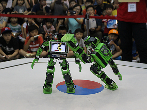 The 2015 Intelligent SoC Robot War Finals
The final round of the 2015 Intelligent SoC (System on Chip) Robot War took place from October 29, 2015 to November 1, 2015 at Kintex in Ilsan, Korea.
A “SoC robot” refers to an intelligent robot capable of autonomous object recognition and decision making by employing advanced semiconductor and information technology.
First hosted in 2002, the Intelligent SoC Robot War cultivates top talents in the field of semiconductors and seeks to revitalize Korea’s information technology (IT) and semiconductor industries.
The event consists of two competitions: HURO and the Tae Kwon Do Robot.
In the HURO competition, participating robots sequentially complete eight assignments without outside controls. Whichever robot finishes the highest number of tasks and spends the shortest amount of time for the completion of assignments wins the competition.
At the HURO competition, a SoC robot overcomes obstacles.
The Tae Kwon Do Robot competition includes Korea’s traditional martial arts into robotics. Here, the winner is selected by sparring between a pair of competitors. The camera attached to the robot’s head recognizes the position of the opponent and the distance between them. From that, the robot takes actions such as punching or kicking.
Two robots are vying for the title of the Tae Kwon Do Robot.
This year, 570 people from 104 teams from all over the nation applied, and after preliminaries, 26 teams entered the finals.
The winners of the HURO and Tae Kwon Do Robot competitions receive awards from the president and prime minister of Korea, respectively.
The Chairman of the Intelligent SoC Robot War, Professor Hoi-Jun Yoo of Electrical Engineering Department at KAIST, said,
“Korea’s strength in semiconductors and information technology can serve as a great potential to advance the development of intelligent robots. We hope that our experiences in this competition will allow Korea to excel in this field.”
2015.11.01 View 10116
 -
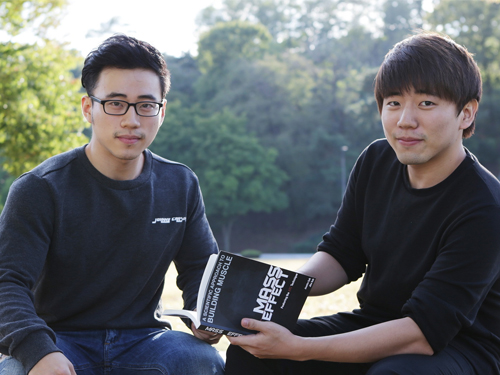 Two Undergraduate KAIST Students Publish a Book on Health Management
Joonho Suh of the Aerospace Engineering Department and Jiho Suh of the Mechanical Engineering Department are both brothers and undergraduates at KAIST.
The Suh brothers, who are three years apart, have recently published a self-help book in English on staying healthy entitled “A Scientific Approach to Building Muscle: Mass Effect.”
The book introduces techniques to build muscles, adapting them from an engineering concept called "Active Torque Control (ACT)," the management of turning forces imposed on a vehicle. Just as ACT influences the performance of a vehicle, good exercise involves the right degree of body angles and the right direction of body movements to keep the best posture necessary for burning calories and strengthening muscles.
In the book, they also suggest healthy diet plans based on scientific knowledge and data that the writers borrowed from such fields as anatomy, physiology, and motor mechanics to maintain a healthy weight.
Joonho Suh said,
“If we understand the mechanism of how our body works, the chances are high we will have good muscle tone and a balanced diet. We used a great deal of scientific knowledge and turned it into a health management program that can be customized per individual needs.”
The younger brother, Jiho, added,
“In fact, we applied our methods in the book to beginners who took weight training and fitness for one hour a day for one month, we learned that their muscle mass increased by 1-1.5 kg while losing body fat by 2-3 kg.”
The brothers said they planned to publish a Korean language version of the book next year.
The authors of "Mass Effect": Joonho Suh (left) and Jiho Suh (right)
2015.10.26 View 8478
 -
 Establishment of System Metabolic Engineering Strategies
Although conventional petrochemical processes have generated chemicals and materials which have been useful to mankind, they have also triggered a variety of environmental problems including climate change and relied too much on nonrenewable natural resources. To ameliorate this, researchers have actively pursued the development of industrial microbial strains around the globe in order to overproduce industrially useful chemicals and materials from microbes using renewable biomass. This discipline is called metabolic engineering.
Thanks to advances in genetic engineering and our knowledge of cellular metabolism, conventional metabolic engineering efforts have succeeded to a certain extent in developing microbial strains that overproduce bioproducts at an industrial level. However, many metabolic engineering projects launched in academic labs do not reach commercial markets due to a failure to fully integrate industrial bioprocesses.
In response to this, Distinguished Professor Sang Yup Lee and Dr. Hyun Uk Kim, both from the Department of Chemical and Biomolecular Engineering at KAIST, have recently suggested ten general strategies of systems metabolic engineering to successfully develop industrial microbial strains. Systems metabolic engineering differs from conventional metabolic engineering by incorporating traditional metabolic engineering approaches along with tools of other fields, such as systems biology, synthetic biology, and molecular evolution.
The ten strategies of systems metabolic engineering have been featured in Nature Biotechnology released online in October 2015, which is entitled "Systems strategies for developing industrial microbial strains."
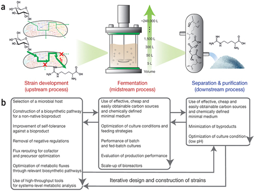
The strategies cover economic, state-of-the-art biological techniques and traditional bioprocess aspects. Specifically, they consist of: 1) project design including economic evaluation of a target bioproduct; 2) selection of host strains to be used for overproduction of a bioproduct; 3) metabolic pathway reconstruction for bioproducts that are not naturally produced in the selected host strains; 4) increasing tolerance of a host strain against the bioproduct; 5) removing negative regulatory circuits in the microbial host limiting overproduction of a bioproduct; 6) rerouting intracellular fluxes to optimize cofactor and precursor availability necessary for the bioproduct formation; 7) diagnosing and optimizing metabolic fluxes towards product formation; 8) diagnosis and optimization of microbial culture conditions including carbon sources; 9) system-wide gene manipulation to further increase the host strain's production performance using high-throughput genome-scale engineering and computational tools; and 10) scale-up fermentation of the developed strain and diagnosis for the reproducibility of the strain's production performance.
These ten strategies were articulated with successful examples of the production of L-arginine using Corynebacterium glutamicum, 1,4-butanediol using Escherichia coli, and L-lysine and bio-nylon using C. glutamicum.
Professor Sang Yup Lee said, "At the moment, the chance of commercializing microbial strains developed in academic labs is very low. The strategies of systems metabolic engineering outlined in this analysis can serve as guidelines when developing industrial microbial strains. We hope that these strategies contribute to improving opportunities to commercialize microbial strains developed in academic labs with drastically reduced costs and efforts, and that a large fraction of petroleum-based processes will be replaced with sustainable bioprocesses."
Lee S. Y. & Kim, H. U. Systems Strategies for Developing Industrial Microbial Strains. Nature Biotechnology (2015).
This work was supported by the Technology Development Program to Solve Climate Change on Systems Metabolic Engineering for Biorefineries (NRF-2012M1A2A2026556) and by the Intelligent Synthetic Biology Center through the Global Frontier Project (2011-0031963) from the Ministry of Science, ICT and Future Planning (MSIP), Korea, and through the National Research Foundation (NRF) of Korea. This work was also supported by the Novo Nordisk Foundation.
Picture: Concept of the Systems Metabolic Engineering Framework
(a) Three major bioprocess stages (b) Considerations in systems metabolic engineering to optimize the whole bioprocess. List of considerations for the strain development and fermentation contribute to improving microbial strain's production performance (red), whereas those for the separation and purification help in reducing overall operation costs by facilitating the downstream process (blue). Some of the considerations can be repeated in the course of systems metabolic engineering.
2015.10.19 View 11928
 -
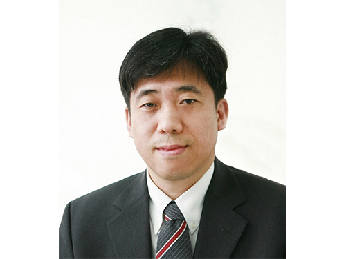 Professor Ki-Jun Jeong Wins the 2015 Dam Yeun Academic Award
The 11th Dam Yeun Academic Award presented by the Korean Society for Biotechnology and Bioengineering (KSBB) to a biologist under 45 years old went to Professor Ki-Jun Jeong of the Chemical and Biomolecular Engineering Department at KAIST.
The award ceremony took place on October 13, 2015, at the annual conference of KSBB held at Songdo Convensia in Incheon City.
Each year KSBB announces the recipient of the award based on the publications by researchers in the last five years at peer-reviewed international journals or KSBB Journal as well as the record of patent registration and technology transfers.
Professor Jeong is recognized for his pioneering research in protein, antibody, cellular engineering, and protein displays and chips.
2015.10.19 View 10689