Nano
-
 Professor Il-Doo Kim Recevies the Song-gok Award
Professor Il-Doo Kim from the Department of Materials Science and Engineering at KAIST received the 20th Song-gok Science and Technology Award from Korea Institute of Science and Technology (KSIT).
The Song-gok Science and Technology Award was established to praise the accomplishments of the first president, Hyung-seop Choi, whose penname is Song-gok. The award selects a recipient in the field of materials and technology every other year.
Professor Kim, in recognition of his outstanding research and contributions to materials science in Korea, received the award during the 52nd anniversary ceremony of KIST on February 9.
Professor Kim focuses on developing nanofiber gas sensors for diagnosing disease in advance by analyzing exhaled biomarkers with electrospinning technology.
He has published more than 211 papers and has recorded more than 9,650 citations and 50 h-index.
Professor Kim has registered 107 patents and applied 38 patents in Korea while registering 29 patents and applying 16 patents overseas. Also, he transferred four technologies in 2017.
Professor Kim is recognized as one of the researchers who is leading nanofiber technology. On January 17, he made a keynote speech at the 5th International Conference on Electrospinning, which was his fourth keynote speech at that conference.
Moreover, he received the Technology Innovation Award at the College of Engineering, KAIST on December 19, 2017.
Professor Kim said, “It is my great honor to receive the Song-gok Science and Technology Award. I would like to bring distinction to KAIST by taking the lead in the commercializing a nanofiber-based highly sensitive nanosensors, diversifying and commercializing technology using nanofiber.”
2018.02.13 View 9683
Professor Il-Doo Kim Recevies the Song-gok Award
Professor Il-Doo Kim from the Department of Materials Science and Engineering at KAIST received the 20th Song-gok Science and Technology Award from Korea Institute of Science and Technology (KSIT).
The Song-gok Science and Technology Award was established to praise the accomplishments of the first president, Hyung-seop Choi, whose penname is Song-gok. The award selects a recipient in the field of materials and technology every other year.
Professor Kim, in recognition of his outstanding research and contributions to materials science in Korea, received the award during the 52nd anniversary ceremony of KIST on February 9.
Professor Kim focuses on developing nanofiber gas sensors for diagnosing disease in advance by analyzing exhaled biomarkers with electrospinning technology.
He has published more than 211 papers and has recorded more than 9,650 citations and 50 h-index.
Professor Kim has registered 107 patents and applied 38 patents in Korea while registering 29 patents and applying 16 patents overseas. Also, he transferred four technologies in 2017.
Professor Kim is recognized as one of the researchers who is leading nanofiber technology. On January 17, he made a keynote speech at the 5th International Conference on Electrospinning, which was his fourth keynote speech at that conference.
Moreover, he received the Technology Innovation Award at the College of Engineering, KAIST on December 19, 2017.
Professor Kim said, “It is my great honor to receive the Song-gok Science and Technology Award. I would like to bring distinction to KAIST by taking the lead in the commercializing a nanofiber-based highly sensitive nanosensors, diversifying and commercializing technology using nanofiber.”
2018.02.13 View 9683 -
 Expanding Gas Storage Capacity of Nanoporous Materials
A KAIST research team led by Professor Jihan Kim of the Department of Chemical and Biomolecular Engineering has successfully proposed a rational defect engineering methodology that can greatly enhance the gas storage capacity of nanoporous materials. The team conducted a high-throughput computational screening of a large experimental metal-organic framework database to identify 13 candidate materials that could experience significant methane uptake enhancement with only a small proportion of linker vacancy defects.
This research was published online on November 16 in Nature Communications, with M.S. candidate Sanggyu Chong from KAIST as the first author and post-doctorate researcher Günther Thiele from the Department of Chemistry at UC Berkeley as a contributing author.
Metal-organic frameworks, hereinafter MOF, are crystalline nanoporous materials that are comprised of metal clusters and organic linkers continuously bound together by coordination bonds. Due to their ultrahigh surface areas and pore volumes, they have been widely studied for various energy and environment applications.
Similar to other crystalline materials, MOFs are never perfectly crystalline and are likely to contain several different types of defects within their crystalline structures. Among these defects, linker vacancy defects, or the random absence of linker vacancies in their designated bonding positions, are known to be controllable by practicing careful control over the synthesis conditions.
The research team combined the concepts of rational defect engineering over the linker vacancy defects and the potential presence of inaccessible pores within MOFs to propose a methodology where controlled the introduction of linker vacancy defects could lead to a dramatic enhancement in gas adsorption and storage capacities.
The study utilized a Graphic Processing Unit (GPU) code developed by Professor Kim in a high-throughput computational screening of 12,000 experimentally synthesized MOFs to identify the structures with significant amounts of pores that were inaccessible for methane. In determining the presence of inaccessible pores, a flood-fill algorithm was performed over the energy-low regions of the structure, which is the same algorithm used for filling an area with color in Microsoft Paint.
For the MOFs with significant amounts of inaccessible pores, as determined from the screening, the research team emulated linker vacancy defects in their crystalline structures so that the previously inaccessible pores would be newly merged into the main adsorption channel with the introduction of defects for additional surface area and pore volume available for adsorption. The research team successfully identified 13 structures that would experience up to a 55.56% increase in their methane uptake with less than 8.33% of the linker vacancy defects.
The research team believes that this rational defect engineering scheme can be further utilized for many other applications in areas such as selective adsorption of an adsorbate from a gas mixture and the semi-permanent capture of gas molecules.
This research was conducted with the support of the Mid-career Research Program of the National Research Foundation of Korea.
Figure1. A diagram for flood fill algorithm and example of identification of inaccessible regions within the MOFs, using the flood fill algorithm
Figure2. Methane energy contours before and after detect introduction
2017.12.04 View 8696
Expanding Gas Storage Capacity of Nanoporous Materials
A KAIST research team led by Professor Jihan Kim of the Department of Chemical and Biomolecular Engineering has successfully proposed a rational defect engineering methodology that can greatly enhance the gas storage capacity of nanoporous materials. The team conducted a high-throughput computational screening of a large experimental metal-organic framework database to identify 13 candidate materials that could experience significant methane uptake enhancement with only a small proportion of linker vacancy defects.
This research was published online on November 16 in Nature Communications, with M.S. candidate Sanggyu Chong from KAIST as the first author and post-doctorate researcher Günther Thiele from the Department of Chemistry at UC Berkeley as a contributing author.
Metal-organic frameworks, hereinafter MOF, are crystalline nanoporous materials that are comprised of metal clusters and organic linkers continuously bound together by coordination bonds. Due to their ultrahigh surface areas and pore volumes, they have been widely studied for various energy and environment applications.
Similar to other crystalline materials, MOFs are never perfectly crystalline and are likely to contain several different types of defects within their crystalline structures. Among these defects, linker vacancy defects, or the random absence of linker vacancies in their designated bonding positions, are known to be controllable by practicing careful control over the synthesis conditions.
The research team combined the concepts of rational defect engineering over the linker vacancy defects and the potential presence of inaccessible pores within MOFs to propose a methodology where controlled the introduction of linker vacancy defects could lead to a dramatic enhancement in gas adsorption and storage capacities.
The study utilized a Graphic Processing Unit (GPU) code developed by Professor Kim in a high-throughput computational screening of 12,000 experimentally synthesized MOFs to identify the structures with significant amounts of pores that were inaccessible for methane. In determining the presence of inaccessible pores, a flood-fill algorithm was performed over the energy-low regions of the structure, which is the same algorithm used for filling an area with color in Microsoft Paint.
For the MOFs with significant amounts of inaccessible pores, as determined from the screening, the research team emulated linker vacancy defects in their crystalline structures so that the previously inaccessible pores would be newly merged into the main adsorption channel with the introduction of defects for additional surface area and pore volume available for adsorption. The research team successfully identified 13 structures that would experience up to a 55.56% increase in their methane uptake with less than 8.33% of the linker vacancy defects.
The research team believes that this rational defect engineering scheme can be further utilized for many other applications in areas such as selective adsorption of an adsorbate from a gas mixture and the semi-permanent capture of gas molecules.
This research was conducted with the support of the Mid-career Research Program of the National Research Foundation of Korea.
Figure1. A diagram for flood fill algorithm and example of identification of inaccessible regions within the MOFs, using the flood fill algorithm
Figure2. Methane energy contours before and after detect introduction
2017.12.04 View 8696 -
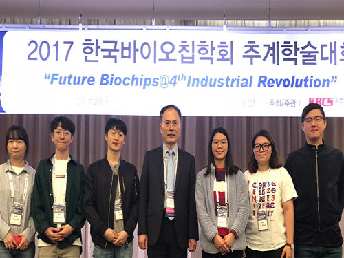 Professor Je-Kyun Park, Awarded by The Korean BioChip Society
On November 9, Je-Kyun Park from the Department of Bio and Brain Engineering at KAIST received an award from the 2017 Fall Meeting of The Korean BioChip Society held in Paradise Hotel Busan, Korea. This year’s meeting recognized Professor Park for developing lab-on-a-chip and microfluidic analytical technologies.
The Korean BioChip Society is a corporation of biochip professional established in 2006 for the development of biochip technology. Every year, the Society selects a recipient based on the nominees’ academic achievements and contributions to bio-fusion industry.
Professor Park served on the international editorial boards of renowned international journals in related fields, including Biosensors and Bioelectronics and Lab on a Chip. He was also the Committee Chairman of MicroTas in 2015.
2017.11.22 View 9675
Professor Je-Kyun Park, Awarded by The Korean BioChip Society
On November 9, Je-Kyun Park from the Department of Bio and Brain Engineering at KAIST received an award from the 2017 Fall Meeting of The Korean BioChip Society held in Paradise Hotel Busan, Korea. This year’s meeting recognized Professor Park for developing lab-on-a-chip and microfluidic analytical technologies.
The Korean BioChip Society is a corporation of biochip professional established in 2006 for the development of biochip technology. Every year, the Society selects a recipient based on the nominees’ academic achievements and contributions to bio-fusion industry.
Professor Park served on the international editorial boards of renowned international journals in related fields, including Biosensors and Bioelectronics and Lab on a Chip. He was also the Committee Chairman of MicroTas in 2015.
2017.11.22 View 9675 -
 Material-Independent Nanocoating Antimicrobial Spray Significantly Extends the Shelf Life of Produce
The edible coating on produce has drawn a great deal of attention in the food and agricultural industry. It could not only prolong postharvest shelf life of produce against external changes in the environment but also provide additional nutrients to be useful for human health. However, most versions of the coating have had intrinsic limitations in their practical application. First, highly specific interactions between coating materials and target surfaces are required for a stable and durable coating. Even further, the coating of bulk substrates, such as fruits, is time consuming or is not achievable in the conventional solution-based coating. In this respect, material-independent and rapid coating strategies are highly demanded.
The research team led by Professor Insung Choi of the Department of Chemistry developed a sprayable nanocoating technique using plant-derived polyphenol that can be applied to any surface. This new nanocoating process can be completed in seconds to form nanometer-thick films, allowing for the coating of commodity goods, such as shoe insoles and fruits, in a controlled fashion. For example, spray-coated mandarin oranges and strawberries show significantly-prolonged postharvest shelf life, suggesting the practical potential in edible coatings of perishable produce.
The technology has been patented and is currently being commercialized for widespread use as a means of preserving produce. The research results have recently been published in Scientific Reports on Aug 1.
Polyphenols, a metabolite of photosynthesis, possess several hydroxyl groups and are found in a large number of plants showing excellent antioxidant properties. They have been widely used as a nontoxic food additive and are known to exhibit antibacterial, as well as potential anti-carcinogenic capabilities. Polyphenols can also be used with iron ions, which are naturally found in the body, to form an adhesive complex, which has been used in leather tanning, ink, etc.
The research team combined these chemical properties of polyphenol-iron complexes with spray techniques to develop their nanocoating technology. Compared to conventional immersion coating methods, which dip substrates in specialized coating solutions, this spray technique can coat the select areas more quickly. The spray also prevents cross contamination, which is a big concern for immersion methods. The research team has showcased the spray’s ability to coat a variety of different materials, including metals, plastics, glass, as well as textile fabrics. The polyphenol complex has been used to form antifogging films on corrective lenses, as well as antifungal treatments for shoe soles, demonstrating the versatility of their technique.
Furthermore, the spray has been used to coat produce with a naturally antibacterial, edible film. The coatings significantly improved the shelf life of tangerines and strawberries, preserving freshness beyond 28 days and 58 hours, respectively. (Uncoated fruit decomposed and became moldy under the same conditions). See the image below.
a –I, II: Uncoated and coated tangerines incubated for 14 and 28 days in daily-life settings
b –I: Uncoated and coated strawberries incubated for 58 hours in daily-life settings
b –II: Statistical investigation of the resulting edibility.
Professor Choi said, “Nanocoating technologies are still in their infancy, but they have untapped potential for exciting applications. As we have shown, nanocoatings can be easily adapted for several different uses, and the creative combination of existing nanomaterials and coating methods can synergize to unlock this potential.”
2017.08.10 View 10057
Material-Independent Nanocoating Antimicrobial Spray Significantly Extends the Shelf Life of Produce
The edible coating on produce has drawn a great deal of attention in the food and agricultural industry. It could not only prolong postharvest shelf life of produce against external changes in the environment but also provide additional nutrients to be useful for human health. However, most versions of the coating have had intrinsic limitations in their practical application. First, highly specific interactions between coating materials and target surfaces are required for a stable and durable coating. Even further, the coating of bulk substrates, such as fruits, is time consuming or is not achievable in the conventional solution-based coating. In this respect, material-independent and rapid coating strategies are highly demanded.
The research team led by Professor Insung Choi of the Department of Chemistry developed a sprayable nanocoating technique using plant-derived polyphenol that can be applied to any surface. This new nanocoating process can be completed in seconds to form nanometer-thick films, allowing for the coating of commodity goods, such as shoe insoles and fruits, in a controlled fashion. For example, spray-coated mandarin oranges and strawberries show significantly-prolonged postharvest shelf life, suggesting the practical potential in edible coatings of perishable produce.
The technology has been patented and is currently being commercialized for widespread use as a means of preserving produce. The research results have recently been published in Scientific Reports on Aug 1.
Polyphenols, a metabolite of photosynthesis, possess several hydroxyl groups and are found in a large number of plants showing excellent antioxidant properties. They have been widely used as a nontoxic food additive and are known to exhibit antibacterial, as well as potential anti-carcinogenic capabilities. Polyphenols can also be used with iron ions, which are naturally found in the body, to form an adhesive complex, which has been used in leather tanning, ink, etc.
The research team combined these chemical properties of polyphenol-iron complexes with spray techniques to develop their nanocoating technology. Compared to conventional immersion coating methods, which dip substrates in specialized coating solutions, this spray technique can coat the select areas more quickly. The spray also prevents cross contamination, which is a big concern for immersion methods. The research team has showcased the spray’s ability to coat a variety of different materials, including metals, plastics, glass, as well as textile fabrics. The polyphenol complex has been used to form antifogging films on corrective lenses, as well as antifungal treatments for shoe soles, demonstrating the versatility of their technique.
Furthermore, the spray has been used to coat produce with a naturally antibacterial, edible film. The coatings significantly improved the shelf life of tangerines and strawberries, preserving freshness beyond 28 days and 58 hours, respectively. (Uncoated fruit decomposed and became moldy under the same conditions). See the image below.
a –I, II: Uncoated and coated tangerines incubated for 14 and 28 days in daily-life settings
b –I: Uncoated and coated strawberries incubated for 58 hours in daily-life settings
b –II: Statistical investigation of the resulting edibility.
Professor Choi said, “Nanocoating technologies are still in their infancy, but they have untapped potential for exciting applications. As we have shown, nanocoatings can be easily adapted for several different uses, and the creative combination of existing nanomaterials and coating methods can synergize to unlock this potential.”
2017.08.10 View 10057 -
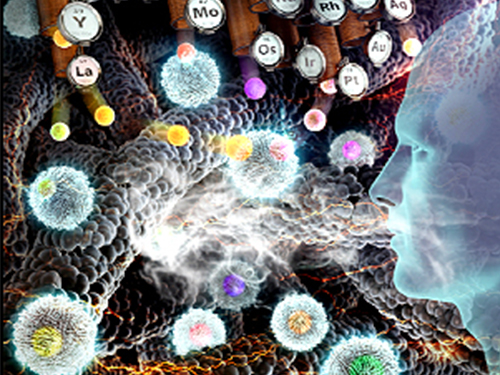 Innovative Nanosensor for Disease Diagnosis
(Figure 1. Sensing Device)
(Figure 2. Protein templating route)
Breath pattern recognition is a futuristic diagnostic platform. Simple characterizing target gas concentrations of human exhaled breath will lead to diagnose of the disease as well as physical condition.
A research group under Prof. Il-Doo Kim in the Department of Materials Science has developed diagnostic sensors using protein-encapsulated nanocatalysts, which can diagnose certain diseases by analyzing human exhaled breath. This technology enables early monitoring of various diseases through pattern recognition of biomarker gases related to diseases in human exhalation.
The protein-templated catalyst synthesis route is very simple and versatile for producing not only a single component of catalytic nanoparticles, but also diverse heterogeneous intermetallic catalysts with sizes less than 3 nm. The research team has developed ever more sensitive and selective chemiresistive sensors that can potentially diagnose specific diseases by analyzing exhaled breath gases.
The results of this study, which were contributed by Dr. Sang-Joon Kim and Dr. Seon-Jin Choi as first authors were selected as the cover-featured article in the July issue of 'Accounts of Chemical Research,' an international journal of the American Chemical Society.
In human breath, diverse components are found including water vapor, hydrogen, acetone, toluene, ammonia, hydrogen sulfide, and carbon monoxide, which are more excessively exhaled from patients. Some of these components are closely related to diseases such as asthma, lung cancer, type 1 diabetes mellitus, and halitosis.
Breath analysis for disease diagnosis started from capturing exhaled breaths in a Tedlar bag and subsequently the captured breath gases were injected into a miniaturized sensor system, similar to an alcohol detector. It is possible to analyze exhaled breath very rapidly with a simple analyzing process. The breath analysis can detect trace changes in exhaled breath components, which contribute to early diagnosis of diseases.
However, technological advances are needed to accurately analyze gases in the breath, which occur at very low levels, from 1 ppb to 1 ppm. In particular, it has been a critical challenge for chemiresistive type chemical sensors to selectively detect specific biomarkers in thousands of interfering gases including humid vapor.
Conventionally, noble metallic catalysts such as platinum and palladium have been functionalized onto metal oxide sensing layers. However, the gas sensitivity was not enough to detect ppb-levels of biomarker species in exhaled breath.
To overcome the current limitations, the research team utilized nanoscale protein (apoferritin) in animals as sacrificial templates. The protein templates possess hollow nanocages at the core site and various alloy catalytic nanoparticles can be encapsulated inside the protein nanocages.
The protein nanocages are advantageous because a nearly unlimited number of material compositions in the periodic table can be assembled for the synthesis of heterogeneous catalytic nanoparticles. In addition, intermetallic nanocatalysts with a controlled atomic ratio of two different elements can be achieved using the protein nanocages, which is an innovative strategy for finding new types of catalysts. For example, highly efficient platinum-based catalysts can be synthesized, such as platinum-palladium (PtPd), platinum-nickel (PtNi), platinum-ruthenium (PtRu), and platinum-yttrium (PtY).
The research team developed outstanding sensing layers consisting of metal oxide nanofibers functionalized by the heterogeneous catalysts with large and highly-porous surface areas, which are especially optimized for selective detection of specific biomarkers. The biomarker sensing performance was improved approximately 3~4-fold as compared to the conventional single component of platinum and palladium catalysts-loaded nanofiber sensors. In particular, 100-fold resistance transitions toward acetone (1 ppm) and hydrogen sulfide (1 ppm) were observed in exhaled breath sensors using the heterogeneous nanocatalysts, which is the best performance ever reported in literature.
The research team developed a disease diagnosis platform that recognizes individual breathing patterns by using a multiple sensor array system with diverse sensing layers and heterogeneous catalysts, so that the people can easily identify health abnormalities. Using a 16-sensor array system, physical conditions can be continuously monitored by analyzing concentration changes of biomarkers in exhaled breath gases.
Prof. Kim said, “New types of heterogeneous nanocatalysts were synthesized using protein templates with sizes around 2 nm and functionalized on various metal oxide nanofiber sensing layers. The established sensing libraries can detect biomarker species with high sensitivity and selectivity.” He added, “the new and innovative breath gas analysis platform will be very helpful for reducing medical expenditures and continuous monitoring of physical conditions”
Patents related to this technology were licensed to two companies in March and June this year.
2017.07.19 View 11476
Innovative Nanosensor for Disease Diagnosis
(Figure 1. Sensing Device)
(Figure 2. Protein templating route)
Breath pattern recognition is a futuristic diagnostic platform. Simple characterizing target gas concentrations of human exhaled breath will lead to diagnose of the disease as well as physical condition.
A research group under Prof. Il-Doo Kim in the Department of Materials Science has developed diagnostic sensors using protein-encapsulated nanocatalysts, which can diagnose certain diseases by analyzing human exhaled breath. This technology enables early monitoring of various diseases through pattern recognition of biomarker gases related to diseases in human exhalation.
The protein-templated catalyst synthesis route is very simple and versatile for producing not only a single component of catalytic nanoparticles, but also diverse heterogeneous intermetallic catalysts with sizes less than 3 nm. The research team has developed ever more sensitive and selective chemiresistive sensors that can potentially diagnose specific diseases by analyzing exhaled breath gases.
The results of this study, which were contributed by Dr. Sang-Joon Kim and Dr. Seon-Jin Choi as first authors were selected as the cover-featured article in the July issue of 'Accounts of Chemical Research,' an international journal of the American Chemical Society.
In human breath, diverse components are found including water vapor, hydrogen, acetone, toluene, ammonia, hydrogen sulfide, and carbon monoxide, which are more excessively exhaled from patients. Some of these components are closely related to diseases such as asthma, lung cancer, type 1 diabetes mellitus, and halitosis.
Breath analysis for disease diagnosis started from capturing exhaled breaths in a Tedlar bag and subsequently the captured breath gases were injected into a miniaturized sensor system, similar to an alcohol detector. It is possible to analyze exhaled breath very rapidly with a simple analyzing process. The breath analysis can detect trace changes in exhaled breath components, which contribute to early diagnosis of diseases.
However, technological advances are needed to accurately analyze gases in the breath, which occur at very low levels, from 1 ppb to 1 ppm. In particular, it has been a critical challenge for chemiresistive type chemical sensors to selectively detect specific biomarkers in thousands of interfering gases including humid vapor.
Conventionally, noble metallic catalysts such as platinum and palladium have been functionalized onto metal oxide sensing layers. However, the gas sensitivity was not enough to detect ppb-levels of biomarker species in exhaled breath.
To overcome the current limitations, the research team utilized nanoscale protein (apoferritin) in animals as sacrificial templates. The protein templates possess hollow nanocages at the core site and various alloy catalytic nanoparticles can be encapsulated inside the protein nanocages.
The protein nanocages are advantageous because a nearly unlimited number of material compositions in the periodic table can be assembled for the synthesis of heterogeneous catalytic nanoparticles. In addition, intermetallic nanocatalysts with a controlled atomic ratio of two different elements can be achieved using the protein nanocages, which is an innovative strategy for finding new types of catalysts. For example, highly efficient platinum-based catalysts can be synthesized, such as platinum-palladium (PtPd), platinum-nickel (PtNi), platinum-ruthenium (PtRu), and platinum-yttrium (PtY).
The research team developed outstanding sensing layers consisting of metal oxide nanofibers functionalized by the heterogeneous catalysts with large and highly-porous surface areas, which are especially optimized for selective detection of specific biomarkers. The biomarker sensing performance was improved approximately 3~4-fold as compared to the conventional single component of platinum and palladium catalysts-loaded nanofiber sensors. In particular, 100-fold resistance transitions toward acetone (1 ppm) and hydrogen sulfide (1 ppm) were observed in exhaled breath sensors using the heterogeneous nanocatalysts, which is the best performance ever reported in literature.
The research team developed a disease diagnosis platform that recognizes individual breathing patterns by using a multiple sensor array system with diverse sensing layers and heterogeneous catalysts, so that the people can easily identify health abnormalities. Using a 16-sensor array system, physical conditions can be continuously monitored by analyzing concentration changes of biomarkers in exhaled breath gases.
Prof. Kim said, “New types of heterogeneous nanocatalysts were synthesized using protein templates with sizes around 2 nm and functionalized on various metal oxide nanofiber sensing layers. The established sensing libraries can detect biomarker species with high sensitivity and selectivity.” He added, “the new and innovative breath gas analysis platform will be very helpful for reducing medical expenditures and continuous monitoring of physical conditions”
Patents related to this technology were licensed to two companies in March and June this year.
2017.07.19 View 11476 -
 KAIST Nanosatellite LINK Launched to the ISS
Courtesy: United Launch Alliance
The KAIST nanosatellite LINK (Little Intelligent Nanosatellite of KAIST) was successfully launched on an Atlas V booster aboard the NASA CRS-7 Mission on April 18 at Space Launch Complex 41, Cape Canaveral Air Force Station in Florida. The KAIST nanosatellite was developed by the research team led by Professor Hyochoong Bang of the Department of Aerospace Engineering.
Aboard the flight to the ISS (International Space Station) were 28 satellites including LINK. They are part of the QB50 Project, an international educational initiative which aims to deploy an array of CubeSat-mounted sensors into Earth’s thermosphere. The project is funded by the European Commission and managed by the von Karman Institute for Fluid Dynamics in Belgium.
The small satellites are hitching a lift into orbit aboard the unmanned resupply spacecraft Cygnus, with a total mass of 83 kilograms. Built to CubeSat specifications, Cygnus will deploy four of the spacecraft following its departure from the space station. LINK will conduct its scientific mission for three months at the station.
The majority of QB50 satellites carry one of three standard instrument packages, consisting of a primary instrument and an array of thermistors, thermocouples, and resistant temperature detectors. LINK is a two-unit CubeSat and weighs two kilograms. It carries an ion-neutral mass spectrometer (INMS), which measures the mass of ions and neutral atoms, as the primary payload of the QB50 project. The secondary payload is two Langmuir probes, which are in-house sensors (m-NLP) developed by Professor Kyong Wook Min’s team of the Department of Physics at KAIST. These are all geared toward collecting long-term continuous in-situ measurements of conditions in Earth’s lower thermosphere.
Professor Bang said, “The QB50 Project is being used for educational purposes. However, the LINK launch will bring a new breakthrough toward collecting information on Earth’s lower thermosphere. Building on these experiences of designing and launching the CubeSat will serve as an opportunity to verify the research results made in our lab firsthand in space.”
(Caption: LINK (Little Intelligent Nanosatellite of KAIST) was launched on an Atlast V booster aboard the NASA CRS-7 Mission on April 18.)
2017.04.25 View 9623
KAIST Nanosatellite LINK Launched to the ISS
Courtesy: United Launch Alliance
The KAIST nanosatellite LINK (Little Intelligent Nanosatellite of KAIST) was successfully launched on an Atlas V booster aboard the NASA CRS-7 Mission on April 18 at Space Launch Complex 41, Cape Canaveral Air Force Station in Florida. The KAIST nanosatellite was developed by the research team led by Professor Hyochoong Bang of the Department of Aerospace Engineering.
Aboard the flight to the ISS (International Space Station) were 28 satellites including LINK. They are part of the QB50 Project, an international educational initiative which aims to deploy an array of CubeSat-mounted sensors into Earth’s thermosphere. The project is funded by the European Commission and managed by the von Karman Institute for Fluid Dynamics in Belgium.
The small satellites are hitching a lift into orbit aboard the unmanned resupply spacecraft Cygnus, with a total mass of 83 kilograms. Built to CubeSat specifications, Cygnus will deploy four of the spacecraft following its departure from the space station. LINK will conduct its scientific mission for three months at the station.
The majority of QB50 satellites carry one of three standard instrument packages, consisting of a primary instrument and an array of thermistors, thermocouples, and resistant temperature detectors. LINK is a two-unit CubeSat and weighs two kilograms. It carries an ion-neutral mass spectrometer (INMS), which measures the mass of ions and neutral atoms, as the primary payload of the QB50 project. The secondary payload is two Langmuir probes, which are in-house sensors (m-NLP) developed by Professor Kyong Wook Min’s team of the Department of Physics at KAIST. These are all geared toward collecting long-term continuous in-situ measurements of conditions in Earth’s lower thermosphere.
Professor Bang said, “The QB50 Project is being used for educational purposes. However, the LINK launch will bring a new breakthrough toward collecting information on Earth’s lower thermosphere. Building on these experiences of designing and launching the CubeSat will serve as an opportunity to verify the research results made in our lab firsthand in space.”
(Caption: LINK (Little Intelligent Nanosatellite of KAIST) was launched on an Atlast V booster aboard the NASA CRS-7 Mission on April 18.)
2017.04.25 View 9623 -
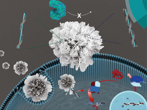 Nuclease-Resistant Hybrid Nanoflowers
An eco-friendly method to synthesize DNA-copper nanoflowers with high load efficiencies, low cytotoxicity, and strong resistance against nucleases has been developed by Professor Hyun Gyu Park in the Department of Chemical and Biomolecular Engineering and his collaborators.
The research team successfully formed a flower-shaped nanostructure in an eco-friendly condition by using interactions between copper ions and DNA containing amide and amine groups. The resulting nanoflowers exhibit high DNA loading capacities in addition to low cytotoxicity.
Flower-shaped nanocrystals called nanoflowers have gained attention for their distinct features of high surface roughness and high surface area to volume ratios. The nanoflowers have been used in many areas including catalysis, electronics, and analytical chemistry.
Of late, research breakthroughs were made in the generation of hybrid inorganic-organic nanoflowers containing various enzymes as organic components. The hybridization with inorganic materials greatly enhanced enzymatic activity, stability, and durability compared to the corresponding free enzymes.
Generally, the formation of protein nanocrystals requires high heat treatment so it has limitations for achieving the high loading capacities of intact DNA.
The research team addressed the issue, focusing on the fact that nucleic acids with well-defined structures and selective recognition properties also contain amide and amine groups in their nucleobases. They proved that flower-like structures could be formed by using nucleic acids as a synthetic template, which paved the way to synthesize the hybrid nanoflowers containing DNA as an organic component in an eco-friendly condition.
The team also confirmed that this synthetic method can be universally applied to any DNA sequences containing amide and amine groups. They said their approach is quite unique considering that the majority of previous works focused on the utilization of DNA as a linker to assemble the nanomaterials. They said the method has several advantageous features. First, the ‘green’ synthetic procedure doesn’t involve any toxic chemicals, and shows low cytotoxicity and strong resistance against nucleases. Second, the obtained nanoflowers exhibit exceptionally high DNA loading capacities.
Above all, such superior features of hybrid nanoflowers enabled the sensitive detection of various molecules including phenol, hydrogen peroxide, and glucose. DNA-copper nanoflowers showed even higher peroxidase activity than those of protein-copper nanoflowers, which may be due to the larger surface area of the flower- shaped structures, creating a greater chance for applying them in the field of sensing of detection of hydrogen peroxide.
The research team expects that their research will create diverse applications in many areas including biosensors and will be further applied into therapeutic applications.
Professor Park said, “The inorganic component in the hybrid nanoflowers not only exhibits low cytotoxicity, but also protects the encapsulated DNA from being cleaved by endonuclease enzymes. Using this feature, the nanostructure will be applied into developing gene therapeutic carriers.”
This research was co-led by Professor Moon Il Kim at Gachon University and KAIST graduate Ki Soo Park, currently a professor at Konkuk University, is the first author. The research was featured as the front cover article of the Journal of Materials Chemistry B on March 28, Issue 12, published by the Royal Society of Chemistry.
The research was funded by the Mid-Career Researcher Support Program of the National Research Foundation of Korea and the Global Frontier Project of the Ministry of Science, ICT & Future Planning.
(Figure: (A) Schematic illustration of the formation of nuclease-resistant DNA–inorganic nanoflowers. (B) SEM images showing time-dependent growth of DNA-nanoflowers. The concentration of A-rich ssDNA (Table S1, ESI†) was 0.25 mM.)
2017.04.14 View 10002
Nuclease-Resistant Hybrid Nanoflowers
An eco-friendly method to synthesize DNA-copper nanoflowers with high load efficiencies, low cytotoxicity, and strong resistance against nucleases has been developed by Professor Hyun Gyu Park in the Department of Chemical and Biomolecular Engineering and his collaborators.
The research team successfully formed a flower-shaped nanostructure in an eco-friendly condition by using interactions between copper ions and DNA containing amide and amine groups. The resulting nanoflowers exhibit high DNA loading capacities in addition to low cytotoxicity.
Flower-shaped nanocrystals called nanoflowers have gained attention for their distinct features of high surface roughness and high surface area to volume ratios. The nanoflowers have been used in many areas including catalysis, electronics, and analytical chemistry.
Of late, research breakthroughs were made in the generation of hybrid inorganic-organic nanoflowers containing various enzymes as organic components. The hybridization with inorganic materials greatly enhanced enzymatic activity, stability, and durability compared to the corresponding free enzymes.
Generally, the formation of protein nanocrystals requires high heat treatment so it has limitations for achieving the high loading capacities of intact DNA.
The research team addressed the issue, focusing on the fact that nucleic acids with well-defined structures and selective recognition properties also contain amide and amine groups in their nucleobases. They proved that flower-like structures could be formed by using nucleic acids as a synthetic template, which paved the way to synthesize the hybrid nanoflowers containing DNA as an organic component in an eco-friendly condition.
The team also confirmed that this synthetic method can be universally applied to any DNA sequences containing amide and amine groups. They said their approach is quite unique considering that the majority of previous works focused on the utilization of DNA as a linker to assemble the nanomaterials. They said the method has several advantageous features. First, the ‘green’ synthetic procedure doesn’t involve any toxic chemicals, and shows low cytotoxicity and strong resistance against nucleases. Second, the obtained nanoflowers exhibit exceptionally high DNA loading capacities.
Above all, such superior features of hybrid nanoflowers enabled the sensitive detection of various molecules including phenol, hydrogen peroxide, and glucose. DNA-copper nanoflowers showed even higher peroxidase activity than those of protein-copper nanoflowers, which may be due to the larger surface area of the flower- shaped structures, creating a greater chance for applying them in the field of sensing of detection of hydrogen peroxide.
The research team expects that their research will create diverse applications in many areas including biosensors and will be further applied into therapeutic applications.
Professor Park said, “The inorganic component in the hybrid nanoflowers not only exhibits low cytotoxicity, but also protects the encapsulated DNA from being cleaved by endonuclease enzymes. Using this feature, the nanostructure will be applied into developing gene therapeutic carriers.”
This research was co-led by Professor Moon Il Kim at Gachon University and KAIST graduate Ki Soo Park, currently a professor at Konkuk University, is the first author. The research was featured as the front cover article of the Journal of Materials Chemistry B on March 28, Issue 12, published by the Royal Society of Chemistry.
The research was funded by the Mid-Career Researcher Support Program of the National Research Foundation of Korea and the Global Frontier Project of the Ministry of Science, ICT & Future Planning.
(Figure: (A) Schematic illustration of the formation of nuclease-resistant DNA–inorganic nanoflowers. (B) SEM images showing time-dependent growth of DNA-nanoflowers. The concentration of A-rich ssDNA (Table S1, ESI†) was 0.25 mM.)
2017.04.14 View 10002 -
 Scholarship in Memory of Professor Shin Endowed by His Family
Professor Joong-Hoon Shin of the Graduate School of Nanoscience and Technology was touted as a genius young scientist who would take the lead in nanoscience technology. After earning degrees from Harvard and the Caltech, he was appointed at KAIST at age 27. He was the youngest professor ever appointed in Korea.
Professor Shin’s outstanding research in the field of semiconductor nano-optics led him to be named as the ‘Scientist of the Year’ for three consecutive years from 2004 by the most prestigious scientist and technology organizations including the Korean Academy Science and Technology, the National Research Foundation of Korea, and the Korean government. However, a fatal car accident last September on the way home from a seminar in Gangwon Province took his life and a promising scholar’s research was left unfinished. He was 47 years old.
Mrs. Young-Eun Hong, the widow of the late Professor Shin, made a 100 million KRW gift to KAIST to establish the ‘Joong-Hoon Shin Scholarship’ on April 7. The scholarship will provide financial assistance to outstanding students of physics and nanoscience.
At the donation ceremony attended by President Sung-Chul Shin, Professor Shin’s colleagues and students, and family members, Mrs. Hong said, “My family would like to help young students achieve their dreams on behalf of my husband. I hope students will remember my husband’s passion and dedication toward his studies for a long time. He was a very hard worker.”
Working at KAIST, Professor Shin made significant achievements in field of semiconductor nano-optics, specializing in silicon photonics and silicon nanocrystal structures. In particular, his research team gained attention reproducing the structure of ‘Morpho butterfly’ wings, which produce the same colors from various angles, using external light as a light source without extra power. Their research led to the creation of original technology dubbed the biomimetics reflective display and was published in Nature in 2012.
Professor Shin’s legacy still endures. In February, a research team under Professor Shin-Hyun Kim of the Department of Chemical and Biomolecular Engineering includingthe late Professor Shin’s doctoral student Seung Yeol Lee, posthumously dedicated their research published on Advanced Materials to Professor Shin. ( click )
KAIST President Sung-Chul Shin, who is also a physicist, said “His passing is a great loss to the whole scientific and technology community, at home and abroad. But Joong-Hoon Shin scholarship will enable the growth and ensure the strength of nanoscience and its education at KAIST. We will uphold Professor Shin’s legacy by doing our best to make KAIST a world-leading university which can create global value.”
Mrs. Hong said she will continue her husband’s academic legacy at his alma maters, Harvard and the Caltech, where he earned his BS in physics and his Ph.D. in applied physics respectively. She said she will start fundraising to establish the Joong-Hoon Shin Scholarship at Harvard and Caltech from July.
(Mrs. Hong poses with President Sung-Chul Shin after donating 100 million KRW for establishing 'Joong-Hoon Shin Scholarship' in memory of her husband on April 7.)
2017.04.10 View 8905
Scholarship in Memory of Professor Shin Endowed by His Family
Professor Joong-Hoon Shin of the Graduate School of Nanoscience and Technology was touted as a genius young scientist who would take the lead in nanoscience technology. After earning degrees from Harvard and the Caltech, he was appointed at KAIST at age 27. He was the youngest professor ever appointed in Korea.
Professor Shin’s outstanding research in the field of semiconductor nano-optics led him to be named as the ‘Scientist of the Year’ for three consecutive years from 2004 by the most prestigious scientist and technology organizations including the Korean Academy Science and Technology, the National Research Foundation of Korea, and the Korean government. However, a fatal car accident last September on the way home from a seminar in Gangwon Province took his life and a promising scholar’s research was left unfinished. He was 47 years old.
Mrs. Young-Eun Hong, the widow of the late Professor Shin, made a 100 million KRW gift to KAIST to establish the ‘Joong-Hoon Shin Scholarship’ on April 7. The scholarship will provide financial assistance to outstanding students of physics and nanoscience.
At the donation ceremony attended by President Sung-Chul Shin, Professor Shin’s colleagues and students, and family members, Mrs. Hong said, “My family would like to help young students achieve their dreams on behalf of my husband. I hope students will remember my husband’s passion and dedication toward his studies for a long time. He was a very hard worker.”
Working at KAIST, Professor Shin made significant achievements in field of semiconductor nano-optics, specializing in silicon photonics and silicon nanocrystal structures. In particular, his research team gained attention reproducing the structure of ‘Morpho butterfly’ wings, which produce the same colors from various angles, using external light as a light source without extra power. Their research led to the creation of original technology dubbed the biomimetics reflective display and was published in Nature in 2012.
Professor Shin’s legacy still endures. In February, a research team under Professor Shin-Hyun Kim of the Department of Chemical and Biomolecular Engineering includingthe late Professor Shin’s doctoral student Seung Yeol Lee, posthumously dedicated their research published on Advanced Materials to Professor Shin. ( click )
KAIST President Sung-Chul Shin, who is also a physicist, said “His passing is a great loss to the whole scientific and technology community, at home and abroad. But Joong-Hoon Shin scholarship will enable the growth and ensure the strength of nanoscience and its education at KAIST. We will uphold Professor Shin’s legacy by doing our best to make KAIST a world-leading university which can create global value.”
Mrs. Hong said she will continue her husband’s academic legacy at his alma maters, Harvard and the Caltech, where he earned his BS in physics and his Ph.D. in applied physics respectively. She said she will start fundraising to establish the Joong-Hoon Shin Scholarship at Harvard and Caltech from July.
(Mrs. Hong poses with President Sung-Chul Shin after donating 100 million KRW for establishing 'Joong-Hoon Shin Scholarship' in memory of her husband on April 7.)
2017.04.10 View 8905 -
 Improving Silver Nanowires for FTCEs with Flash Light Interactions
Flexible transparent conducting electrodes (FTCEs) are an essential element of flexible optoelectronics for next-generation wearable displays, augmented reality (AR), and the Internet of Things (IoTs). Silver nanowires (Ag NWs) have received a great deal of attention as future FTCEs due to their great flexibility, material stability, and large-scale productivity. Despite these advantages, Ag NWs have drawbacks such as high wire-to-wire contact resistance and poor adhesion to substrates, resulting in severe power consumption and the delamination of FTCEs.
A research team led by Professor Keon Jae Lee of the Materials Science and Engineering Department at KAIST and Dr. Hong-Jin Park from BSP Inc., has developed high-performance Ag NWs (sheet resistance ~ 5 Ω/sq, transmittance 90 % at λ = 550 nm) with strong adhesion on plastic (interfacial energy of 30.7 J∙m-2) using flash light-material interactions.
The broad ultraviolet (UV) spectrum of a flash light enables the localized heating at the junctions of nanowires (NWs), which results in the fast and complete welding of Ag NWs. Consequently, the Ag NWs demonstrate six times higher conductivity than that of the pristine NWs. In addition, the near-infrared (NIR) of the flash lamp melted the interface between the Ag NWs and a polyethylene terephthalate (PET) substrate, dramatically enhancing the adhesion force of the Ag NWs to the PET by 310 %.
Professor Lee said, “Light interaction with nanomaterials is an important field for future flexible electronics since it can overcome thermal limit of plastics, and we are currently expanding our research into light-inorganic interactions.”
Meanwhile, BSP Inc., a laser manufacturing company and a collaborator of this work, has launched new flash lamp equipment for flexible applications based on the Professor Lee’s research.
The results of this work entitled “Flash-Induced Self-Limited Plasmonic Welding of Ag NW Network for Transparent Flexible Energy Harvester (DOI: 10.1002/adma.201603473)” were published in the February 2, 2017 issue of Advanced Materials as the cover article.
Professor Lee also contributed an invited review in the same journal of the April 3, 2017 online issue, “Laser-Material Interactions for Flexible Applications (DOI:10.1002/adma.201606586),” overviewing the recent advances in light interactions with flexible nanomaterials.
References
[1] Advanced Materials, February 2, 2017, Flash-Induced Self-Limited Plasmonic Welding of Ag NW network for Transparent Flexible Energy Harvester http://onlinelibrary.wiley.com/doi/10.1002/adma.201603473/epdf
[2] Advanced Materials, April 3, 2017, Laser-Material Interactions for Flexible Applications
http://onlinelibrary.wiley.com/doi/10.1002/adma.201606586/abstract
For further inquiries on research:
keonlee@kaist.ac.kr (Keon Jae Lee), hjpark@bsptech.co.kr (Hong-Jin Park)
Picture 1: Artistic Rendtition of Light Interaction with Nanomaterials
(This image shows flash-induced plasmonic interactions with nanowires to improve silver nanowires (Ag NWs).)
Picture 2: Ag NW/PET Film
(This picture shows the Ag NWs on a polyethylene terephthalate (PET) film after the flash-induced plasmonic thermal process.)
2017.04.05 View 11601
Improving Silver Nanowires for FTCEs with Flash Light Interactions
Flexible transparent conducting electrodes (FTCEs) are an essential element of flexible optoelectronics for next-generation wearable displays, augmented reality (AR), and the Internet of Things (IoTs). Silver nanowires (Ag NWs) have received a great deal of attention as future FTCEs due to their great flexibility, material stability, and large-scale productivity. Despite these advantages, Ag NWs have drawbacks such as high wire-to-wire contact resistance and poor adhesion to substrates, resulting in severe power consumption and the delamination of FTCEs.
A research team led by Professor Keon Jae Lee of the Materials Science and Engineering Department at KAIST and Dr. Hong-Jin Park from BSP Inc., has developed high-performance Ag NWs (sheet resistance ~ 5 Ω/sq, transmittance 90 % at λ = 550 nm) with strong adhesion on plastic (interfacial energy of 30.7 J∙m-2) using flash light-material interactions.
The broad ultraviolet (UV) spectrum of a flash light enables the localized heating at the junctions of nanowires (NWs), which results in the fast and complete welding of Ag NWs. Consequently, the Ag NWs demonstrate six times higher conductivity than that of the pristine NWs. In addition, the near-infrared (NIR) of the flash lamp melted the interface between the Ag NWs and a polyethylene terephthalate (PET) substrate, dramatically enhancing the adhesion force of the Ag NWs to the PET by 310 %.
Professor Lee said, “Light interaction with nanomaterials is an important field for future flexible electronics since it can overcome thermal limit of plastics, and we are currently expanding our research into light-inorganic interactions.”
Meanwhile, BSP Inc., a laser manufacturing company and a collaborator of this work, has launched new flash lamp equipment for flexible applications based on the Professor Lee’s research.
The results of this work entitled “Flash-Induced Self-Limited Plasmonic Welding of Ag NW Network for Transparent Flexible Energy Harvester (DOI: 10.1002/adma.201603473)” were published in the February 2, 2017 issue of Advanced Materials as the cover article.
Professor Lee also contributed an invited review in the same journal of the April 3, 2017 online issue, “Laser-Material Interactions for Flexible Applications (DOI:10.1002/adma.201606586),” overviewing the recent advances in light interactions with flexible nanomaterials.
References
[1] Advanced Materials, February 2, 2017, Flash-Induced Self-Limited Plasmonic Welding of Ag NW network for Transparent Flexible Energy Harvester http://onlinelibrary.wiley.com/doi/10.1002/adma.201603473/epdf
[2] Advanced Materials, April 3, 2017, Laser-Material Interactions for Flexible Applications
http://onlinelibrary.wiley.com/doi/10.1002/adma.201606586/abstract
For further inquiries on research:
keonlee@kaist.ac.kr (Keon Jae Lee), hjpark@bsptech.co.kr (Hong-Jin Park)
Picture 1: Artistic Rendtition of Light Interaction with Nanomaterials
(This image shows flash-induced plasmonic interactions with nanowires to improve silver nanowires (Ag NWs).)
Picture 2: Ag NW/PET Film
(This picture shows the Ag NWs on a polyethylene terephthalate (PET) film after the flash-induced plasmonic thermal process.)
2017.04.05 View 11601 -
 A Transport Technology for Nanowires Thermally Treated at 700 Celsius Degrees
Professor Jun-Bo Yoon and his research team of the Department of Electrical Engineering at KAIST developed a technology for transporting thermally treated nanowires to a flexible substrate and created a high performance device for collecting flexible energy by using the new technology.
Mr. Min-Ho Seo, a Ph.D. candidate, participated in this study as the first author. The results were published online on January 30th in ACS Nano, an international journal in the field of nanoscience and engineering. (“Versatile Transfer of an Ultralong and Seamless Nanowire Array Crystallized at High Temperature for Use in High-performance Flexible Devices,” DOI: 10.1021/acsnano.6b06842)
Nanowires are one of the most representative nanomaterials. They have wire structures with dimensions in nanometers. The nanowires are widely used in the scientific and engineering fields due to their prominent physical and chemical properties that depend on a one-dimensional structure, and their high applicability.
Nanowires have much higher performance if their structure has unique features such as an excellent arrangement and a longer-than-average length. Many researchers are thus actively participating in the research for making nanowires without much difficulty, analyzing them, and developing them for high performance application devices.
Scientists have recently favored a research topic on making nanowires chemically and physically on a flexible substrate and applies the nanowires to a flexible electric device such as a high performance wearable sensor.
The existing technology, however, mixed nanowires from a chemical synthesis with a solution and spread the mixture on a flexible substrate. The resultant distribution was random, and it was difficult to produce a high performance device based on the structural advantages of nanowires. In addition, the technology used a cutting edge nano-process and flexible materials, but this was not economically beneficial. The production of stable materials at a temperature of 700 Celsius degrees or higher is unattainable, a great challenge for the application.
To solve this problem, the research team developed a new nano-transfer technology that combines a silicon nano-grating board with a large surface area and a nano-sacrificial layer process. A nano-sacrificial layer exists between nanowires and a nano-grating board, which acts as the mold for the nano-transfer. The new technology allows the device undergo thermal treatment. After this, the layer disappears when the nanowires are transported to a flexible substrate.
This technology also permits the stable production of nanowires with secured properties at an extremely high temperature. In this case, the nanowires are neatly organized on a flexible substrate. The research team used the technology to manufacture barium carbonate nanowires on top of the flexible substrate. The wires secured their properties at a temperature of 700℃ or above. The team employed the collection of wearable energy to obtain much higher electrical energy than that of an energy collecting device designed based on regular barium titanate nanowires.
The researchers said that their technology is built upon a semiconductor process, known as Physical Vapor Deposition that allows various materials such as ceramics and semiconductors to be used for flexible substrates of nanowires. They expected that high performance flexible electric devices such as flexible transistors and thermoelectric elements can be produced with this method.
Mr. Seo said, “In this study, we transported nanowire materials with developed properties on a flexible substrate and showed an increase in device performance. Our technology will be fundamental to the production of various nanowires on a flexible substrate as well as the feasibility of making high performance wearable electric devices.”
This research was supported by the Leap Research Support Program of the National Research Foundation of Korea.
Fig. 1. Transcription process of new, developed nanowires (a) and a fundamental mimetic diagram of a nano-sacrificial layer (b)
Fig. 2. Transcription results from using gold (AU) nanowires. The categories of the results were (a) optical images, (b) physical signals, (c) cross-sectional images from a scanning electron microscope (SEM), and (d-f) an electric verification of whether the perfectly arranged nanowires were made on a large surface.
Fig. 3. Transcription from using barium titanate (BaTiO3) nanowires. The results were (a) optical images, (b-e) top images taken from an SEM in various locations, and (f, g) property analysis.
Fig. 4. Mimetic diagram of the energy collecting device from using a BaTiO3 nanowire substrate and an optical image of the experiment for the miniature energy collecting device attached to an index finger.
2017.03.22 View 10251
A Transport Technology for Nanowires Thermally Treated at 700 Celsius Degrees
Professor Jun-Bo Yoon and his research team of the Department of Electrical Engineering at KAIST developed a technology for transporting thermally treated nanowires to a flexible substrate and created a high performance device for collecting flexible energy by using the new technology.
Mr. Min-Ho Seo, a Ph.D. candidate, participated in this study as the first author. The results were published online on January 30th in ACS Nano, an international journal in the field of nanoscience and engineering. (“Versatile Transfer of an Ultralong and Seamless Nanowire Array Crystallized at High Temperature for Use in High-performance Flexible Devices,” DOI: 10.1021/acsnano.6b06842)
Nanowires are one of the most representative nanomaterials. They have wire structures with dimensions in nanometers. The nanowires are widely used in the scientific and engineering fields due to their prominent physical and chemical properties that depend on a one-dimensional structure, and their high applicability.
Nanowires have much higher performance if their structure has unique features such as an excellent arrangement and a longer-than-average length. Many researchers are thus actively participating in the research for making nanowires without much difficulty, analyzing them, and developing them for high performance application devices.
Scientists have recently favored a research topic on making nanowires chemically and physically on a flexible substrate and applies the nanowires to a flexible electric device such as a high performance wearable sensor.
The existing technology, however, mixed nanowires from a chemical synthesis with a solution and spread the mixture on a flexible substrate. The resultant distribution was random, and it was difficult to produce a high performance device based on the structural advantages of nanowires. In addition, the technology used a cutting edge nano-process and flexible materials, but this was not economically beneficial. The production of stable materials at a temperature of 700 Celsius degrees or higher is unattainable, a great challenge for the application.
To solve this problem, the research team developed a new nano-transfer technology that combines a silicon nano-grating board with a large surface area and a nano-sacrificial layer process. A nano-sacrificial layer exists between nanowires and a nano-grating board, which acts as the mold for the nano-transfer. The new technology allows the device undergo thermal treatment. After this, the layer disappears when the nanowires are transported to a flexible substrate.
This technology also permits the stable production of nanowires with secured properties at an extremely high temperature. In this case, the nanowires are neatly organized on a flexible substrate. The research team used the technology to manufacture barium carbonate nanowires on top of the flexible substrate. The wires secured their properties at a temperature of 700℃ or above. The team employed the collection of wearable energy to obtain much higher electrical energy than that of an energy collecting device designed based on regular barium titanate nanowires.
The researchers said that their technology is built upon a semiconductor process, known as Physical Vapor Deposition that allows various materials such as ceramics and semiconductors to be used for flexible substrates of nanowires. They expected that high performance flexible electric devices such as flexible transistors and thermoelectric elements can be produced with this method.
Mr. Seo said, “In this study, we transported nanowire materials with developed properties on a flexible substrate and showed an increase in device performance. Our technology will be fundamental to the production of various nanowires on a flexible substrate as well as the feasibility of making high performance wearable electric devices.”
This research was supported by the Leap Research Support Program of the National Research Foundation of Korea.
Fig. 1. Transcription process of new, developed nanowires (a) and a fundamental mimetic diagram of a nano-sacrificial layer (b)
Fig. 2. Transcription results from using gold (AU) nanowires. The categories of the results were (a) optical images, (b) physical signals, (c) cross-sectional images from a scanning electron microscope (SEM), and (d-f) an electric verification of whether the perfectly arranged nanowires were made on a large surface.
Fig. 3. Transcription from using barium titanate (BaTiO3) nanowires. The results were (a) optical images, (b-e) top images taken from an SEM in various locations, and (f, g) property analysis.
Fig. 4. Mimetic diagram of the energy collecting device from using a BaTiO3 nanowire substrate and an optical image of the experiment for the miniature energy collecting device attached to an index finger.
2017.03.22 View 10251 -
 Semiconductor Photonic Nanocavities on Paper Substrates
Professor Yong-Hoon Cho of the Department of Physics and his team at KAIST have developed a semiconductor photonic nanocavity laser that can operate on a paper substrate.
The researchers hope that this novel method, which involves transferring nano-sized photonic crystal particles onto a paper substrate with high absorptiveness, will enable the diagnoses of various diseases by using high-tech semiconductor sensors at low cost.
The results of this research were published in the November 17th, 2016, issue of Advanced Materials.
Photonic crystals, which utilize light as a medium to provide high bandwidths, can transfer large amounts of information. Compared with their electronic counterparts, photonic crystals also consume less energy to operate.
Normally, semiconductor photonic particles require substrates, which play only a passive role in the assembly and endurance of individual, functional photonic components. These substrates, however, are bulky and environmentally hazardous as they are made up of non-biodegradable materials.
The research team overcame these two shortcomings by replacing a semiconductor substrate with standard paper. The substrate’s mass was reduced considerably, and because paper is made from trees, it degrades. Paper can be easily and cheaply acquired from our surroundings, which drastically reduces the unit cost of semiconductors.
In addition, paper possesses superior mechanical characteristics. It is flexible and can be repeatedly folded and unfolded without being torn. These are traits that have long been sought by researchers for existing flexible substrates.
The research team used a micro-sized stamp to detach photonic crystal nanobeam cavities selectively from their original substrate and transfer them onto a new paper substrate. Using this technique, the team removed nanophotonic crystals that had been patterned (using a process of selectively etching circuits onto a substrate) onto a semiconductor substrate with a high degree of integration, and realigned them as desired on a paper substrate.
The nanophotonic crystals that the team combined with paper in this research were 0.5 micrometers in width, 6 micrometers in length, and 0.3 micrometers in height—about one-hundredth of the width of a single hair (0.1 millimeter).
The team also transferred their photonic crystals onto paper with a fluid channel, which proved that it could be used as a refractive index sensor. As can be seen in current commercial pregnancy diagnosis kits, paper has high absorptiveness. Since photonic crystal particles have high sensitivity, they are highly suitable for applications such as sensors.
Professor Cho stated that “by using paper substrates, this technology can greatly contribute to the rising field of producing environmentally-friendly photonic particles” and “by combining inexpensive paper and high-performance photonic crystal sensors, we can obtain low prices as well as designing appropriate technologies with high performance.”
Dr. Sejeong Kim of the Department of Physics participated in this study as the first author, and Professor Kwanwoo Shin of Sogang University and Professor Yong-Hee Lee of KAIST also took part in this research. The research was supported by the National Research Foundation’s Mid-Career Researcher Program, and the Climate Change Research Hub of KAIST.
Figure 1. Illustration of photonic crystal lasers on paper substrates
Figure 2. Photonic crystal resonator laser and refractive index sensor operating on paper substrates
2017.03.01 View 8104
Semiconductor Photonic Nanocavities on Paper Substrates
Professor Yong-Hoon Cho of the Department of Physics and his team at KAIST have developed a semiconductor photonic nanocavity laser that can operate on a paper substrate.
The researchers hope that this novel method, which involves transferring nano-sized photonic crystal particles onto a paper substrate with high absorptiveness, will enable the diagnoses of various diseases by using high-tech semiconductor sensors at low cost.
The results of this research were published in the November 17th, 2016, issue of Advanced Materials.
Photonic crystals, which utilize light as a medium to provide high bandwidths, can transfer large amounts of information. Compared with their electronic counterparts, photonic crystals also consume less energy to operate.
Normally, semiconductor photonic particles require substrates, which play only a passive role in the assembly and endurance of individual, functional photonic components. These substrates, however, are bulky and environmentally hazardous as they are made up of non-biodegradable materials.
The research team overcame these two shortcomings by replacing a semiconductor substrate with standard paper. The substrate’s mass was reduced considerably, and because paper is made from trees, it degrades. Paper can be easily and cheaply acquired from our surroundings, which drastically reduces the unit cost of semiconductors.
In addition, paper possesses superior mechanical characteristics. It is flexible and can be repeatedly folded and unfolded without being torn. These are traits that have long been sought by researchers for existing flexible substrates.
The research team used a micro-sized stamp to detach photonic crystal nanobeam cavities selectively from their original substrate and transfer them onto a new paper substrate. Using this technique, the team removed nanophotonic crystals that had been patterned (using a process of selectively etching circuits onto a substrate) onto a semiconductor substrate with a high degree of integration, and realigned them as desired on a paper substrate.
The nanophotonic crystals that the team combined with paper in this research were 0.5 micrometers in width, 6 micrometers in length, and 0.3 micrometers in height—about one-hundredth of the width of a single hair (0.1 millimeter).
The team also transferred their photonic crystals onto paper with a fluid channel, which proved that it could be used as a refractive index sensor. As can be seen in current commercial pregnancy diagnosis kits, paper has high absorptiveness. Since photonic crystal particles have high sensitivity, they are highly suitable for applications such as sensors.
Professor Cho stated that “by using paper substrates, this technology can greatly contribute to the rising field of producing environmentally-friendly photonic particles” and “by combining inexpensive paper and high-performance photonic crystal sensors, we can obtain low prices as well as designing appropriate technologies with high performance.”
Dr. Sejeong Kim of the Department of Physics participated in this study as the first author, and Professor Kwanwoo Shin of Sogang University and Professor Yong-Hee Lee of KAIST also took part in this research. The research was supported by the National Research Foundation’s Mid-Career Researcher Program, and the Climate Change Research Hub of KAIST.
Figure 1. Illustration of photonic crystal lasers on paper substrates
Figure 2. Photonic crystal resonator laser and refractive index sensor operating on paper substrates
2017.03.01 View 8104 -
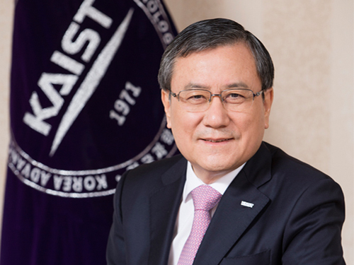 Dr. Sung-Chul Shin Selected 16th President of KAIST
(President Sung-Chul Shin)
The KAIST Board of Trustees elected Professor Sung-Chul Shin of the Department of Physics the 16th president of KAIST on February 21. Professor Shin succeeds President Sung-Mo Kang whose four-year term will end on February 23. He is the first KAIST alumnus to serve as its president.
The Board of Trustees announced, “We believe that Professor Shin’s scientific achievement, outstanding leadership, and clear vision will serve KAIST faculty, students, and staff very well. He will be the best person to help KAIST leap forward in the four years ahead.”
The newly-elected president said, “I am humbled and honored to have been elected to lead such a prestigious institute of Korea. Aiming to be one of the top ten global universities, KAIST will continue to innovate its systems.” Previously, Dr. Shin led the Daegu Gyeongbuk Institute of Science and Technology (DGIST) for six years as president since 2011.
Professor Shin joined the KAIST faculty in 1989. He graduated from Seoul National University and then earned his MS degree in condensed matter physics at KAIST in 1977. After earning his Ph.D. in material physics at Northwestern University in 1984, he worked at Eastman Kodak Research Labs as a senior research scientist for five years.
Before heading to DGIST, President Shin held key administrative positions at KAIST from the early 1990s including dean of planning, dean of the international office, and vice-dean of student affairs. During President Robert Laughlin’s tenure, the first foreign president at KAIST, he served as vice-president for two years from 2004. He also served on the Presidential Advisory Council on Science and Technology of the Korean government as vice chairperson from 2015 to 2016.
A renowned scholar in the field of nanoscience, President Shin’s research focuses on the artificial synthesis and characterization of nonmagnetic materials, magnetic anisotropy, and magneto-optical phenomena. He leads the Laboratory for Nanospinics of Spintronic Materials at KAIST and has published in 290 journals while holding 37 patents.
A fellow in the American Physical Society (APS) since 2008, he was the president of the Korean Physical Society from 2011 to 2012. He has been on the editorial board of J. Magnetism and Magnetic Materials from 2009 and was the first Korean recipient of the Asian Union of Magnetics Societies (AUMS) Award, which recognizes outstanding scientists in the field of magnetics.
President Shin envisions making KAIST’s research and education more competitive through continuing innovation. His innovation efforts will extend to the five key areas of education, research, technology commercialization, globalization, and future planning.
Among his priorities, he emphasizes multidisciplinary studies and leadership training for students. He plans to focus on undeclared major courses for undergraduates to help them expand their experience and exposure to diverse disciplines. This approach will help create well-rounded engineers, scientists, and entrepreneurs by enabling them to develop skills while leveraging a strong connection to the arts, humanities, and social sciences.
To better respond to Industry 4.0, which calls for convergence studies and collaborative work, he proposed establishing a ‘Convergence Innovation System’ by strategically selecting 10 flagship convergence research groups. In order to accelerate the technology commercialization and ecosystem of start-ups, he will strengthen entrepreneurship education, making it a prerequisite requirement for students. President Shin said he will spare no effort to incubate and spin-off ventures in which KAIST technology is being transferred. For globalization efforts, he plans to increase the ratio of foreign faculty from 9 percent to 15 percent, while doubling the current foreign student enrollment ratio of 5 percent. For future strategic innovation, he will implement a long-term innovation strategic plan dubbed ‘Vision 2031.’
2017.02.22 View 13043
Dr. Sung-Chul Shin Selected 16th President of KAIST
(President Sung-Chul Shin)
The KAIST Board of Trustees elected Professor Sung-Chul Shin of the Department of Physics the 16th president of KAIST on February 21. Professor Shin succeeds President Sung-Mo Kang whose four-year term will end on February 23. He is the first KAIST alumnus to serve as its president.
The Board of Trustees announced, “We believe that Professor Shin’s scientific achievement, outstanding leadership, and clear vision will serve KAIST faculty, students, and staff very well. He will be the best person to help KAIST leap forward in the four years ahead.”
The newly-elected president said, “I am humbled and honored to have been elected to lead such a prestigious institute of Korea. Aiming to be one of the top ten global universities, KAIST will continue to innovate its systems.” Previously, Dr. Shin led the Daegu Gyeongbuk Institute of Science and Technology (DGIST) for six years as president since 2011.
Professor Shin joined the KAIST faculty in 1989. He graduated from Seoul National University and then earned his MS degree in condensed matter physics at KAIST in 1977. After earning his Ph.D. in material physics at Northwestern University in 1984, he worked at Eastman Kodak Research Labs as a senior research scientist for five years.
Before heading to DGIST, President Shin held key administrative positions at KAIST from the early 1990s including dean of planning, dean of the international office, and vice-dean of student affairs. During President Robert Laughlin’s tenure, the first foreign president at KAIST, he served as vice-president for two years from 2004. He also served on the Presidential Advisory Council on Science and Technology of the Korean government as vice chairperson from 2015 to 2016.
A renowned scholar in the field of nanoscience, President Shin’s research focuses on the artificial synthesis and characterization of nonmagnetic materials, magnetic anisotropy, and magneto-optical phenomena. He leads the Laboratory for Nanospinics of Spintronic Materials at KAIST and has published in 290 journals while holding 37 patents.
A fellow in the American Physical Society (APS) since 2008, he was the president of the Korean Physical Society from 2011 to 2012. He has been on the editorial board of J. Magnetism and Magnetic Materials from 2009 and was the first Korean recipient of the Asian Union of Magnetics Societies (AUMS) Award, which recognizes outstanding scientists in the field of magnetics.
President Shin envisions making KAIST’s research and education more competitive through continuing innovation. His innovation efforts will extend to the five key areas of education, research, technology commercialization, globalization, and future planning.
Among his priorities, he emphasizes multidisciplinary studies and leadership training for students. He plans to focus on undeclared major courses for undergraduates to help them expand their experience and exposure to diverse disciplines. This approach will help create well-rounded engineers, scientists, and entrepreneurs by enabling them to develop skills while leveraging a strong connection to the arts, humanities, and social sciences.
To better respond to Industry 4.0, which calls for convergence studies and collaborative work, he proposed establishing a ‘Convergence Innovation System’ by strategically selecting 10 flagship convergence research groups. In order to accelerate the technology commercialization and ecosystem of start-ups, he will strengthen entrepreneurship education, making it a prerequisite requirement for students. President Shin said he will spare no effort to incubate and spin-off ventures in which KAIST technology is being transferred. For globalization efforts, he plans to increase the ratio of foreign faculty from 9 percent to 15 percent, while doubling the current foreign student enrollment ratio of 5 percent. For future strategic innovation, he will implement a long-term innovation strategic plan dubbed ‘Vision 2031.’
2017.02.22 View 13043