electronic
-
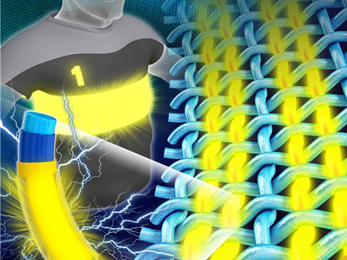 KAIST Develops Fiber-Like Light-Emitting Diodes for Wearable Displays
Professor Kyung-Cheol Choi and his research team from the School of Electrical Engineering at KAIST have developed fiber-like light-emitting diodes (LEDs), which can be applied in wearable displays. The research findings were published online in the July 14th issue of Advanced Electronic Materials.
Traditional wearable displays were manufactured on a hard substrate, which was later attached to the surface of clothes. This technique had limited applications for wearable displays because they were inflexible and ignored the characteristics of fabric.
To solve this problem, the research team discarded the notion of creating light-emitting diode displays on a plane. Instead, they focused on fibers, a component of fabrics, and developed a fiber-like LED that shared the characteristics of both fabrics and displays.
The essence of this technology, the dip-coating process, is to immerse and extract a three dimensional (3-D) rod (a polyethylene terephthalate fiber) from a solution, which functions like thread. Then, the regular levels of organic materials are formed as layers on the thread.
The dip-coating process allows the layers of organic materials to be easily created on the fibers with a 3-D cylindrical structure, which had been difficult in existing processes such as heat-coating process. By controlling of the withdrawal rate of the fiber, the coating's thickness can also be adjusted to the hundreds of thousandths of a nanometer.
The researchers said that this technology would accelerate the commercialization of fiber-based wearable displays because it offers low-cost mass production using roll-to-roll processing, a technology applied to create electronic devices on a roll of flexible plastics or metal foils.
Professor Choi said, “Our research will become a core technology in developing light emitting diodes on fibers, which are fundamental elements of fabrics. We hope we can lower the barrier of wearable displays entering the market.”
The lead author of the published paper, Seon-Il Kwon, added, “This technology will eventually allow the production of wearable displays to be as easy as making clothes.”
Picture 1: The Next Generation Wearable Display Using Fiber-Based Light-Emitting Diodes
Picture 2: Dip-Coating Process to Create Fiber-Based Light-Emitting Diodes
Picture 3: Fiber-Based Light-Emitting Diodes
2015.08.11 View 13451
 -
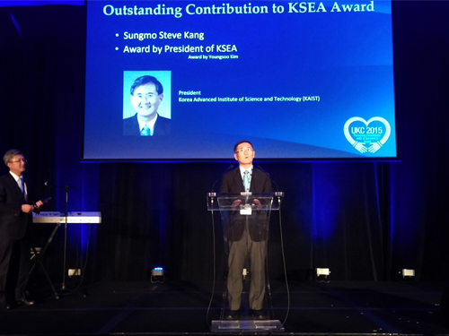 President Steve Kang of KAIST Receives the Outstanding Contribution Award from the Korean-American Scientists and Engineers Association
The Korean-American Scientists and Engineers Association (KSEA), a non-profit Korean professional organization based in the United States with over 6,000 registered members, bestowed upon President Steve Kang of KAIST the 2015 Outstanding Contribution Award.
The award is presented to a person who has made significant contributions to the development of KSEA.
The award ceremony took place during the 2015 US-Korea Conference on Science, Technology, and Entrepreneurship (UKC), which was held on July 30, 2015, at the Hyatt Regency Hotel in Atlanta, Georgia.
The UKC is the flagship conference of KSEA, which takes place every year, and covers science, engineering, technology, industry, entrepreneurship, and leadership. It attracts more than 1,200 participants from the US and Korea. The UKC 2015 was held on July 29-August 1, 2015.
President Kang has participated in UKC conferences over the past few years as a plenary speaker, addressing major issues in science and technology for both nations, and provided generous support for the activities of UKC and KSEA. He also promoted discussions and exchanges of professional knowledge in his field, microelectronics, by organizing fora and symposia.
He addressed the UKC 2015 as a plenary speaker with a speech entitled “Pursuing Excellence with a Servant’s Heart.” President Kang said that good leadership should bring out synergistic contributions from all constituents and achieve excellence under all circumstances. He mentioned one example of good leadership, known as humble leadership, and explained how such leadership played an important role in the development of scientific breakthroughs, such as the world’s premier high-end microprocessor chip sets first produced by his team under extremely high pressure.
2015.08.05 View 7966
 -
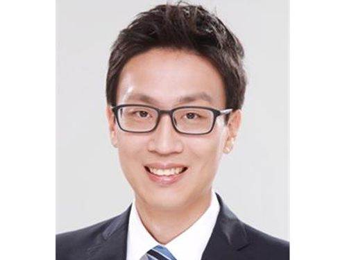 Professor Kyoungsik Yu Receives the Young IT Engineer Award from IEEE and IEIE of Korea
Professor Kyoungsik Yu of KAIST’s Department of Electrical Engineering is the recipient of this year’s Young IT (Information Technology) Engineer Award that was co-hosted by the Institute of Electrical and Electronics Engineers (IEEE), the Institute of Electronics Engineers of Korea (IEIE), and Haedong Science Culture Foundation in Korea. The award was presented on June 22, 2015 at The Ramada Plaza Jeju Hotel on Jeju Island, Korea.
The Young IT Engineer Award is given to emerging scientists who have made significant contributions to the advancement of technology, society, environment, and creative education.
Professor Yu's main research interests are IT, energy, and imaging through miniaturization and integration of optoelectronic devices. His contribution to academic and technological development is reflected in his publication of more than 100 papers in international journals and conferences, which were cited over 2,200 times.
Professor Yu said, “I’m honored to receive this award and am encouraged by it. I also find the award meaningful because the United Nations has designated this year as the “International Year of Light and Light-based Technologies,” the field I have been involved in as a researcher.”
In addition to Korea, the IEEE has jointly hosted and presented this award to researchers in countries such as Chile, Ecuador, Peru, Singapore, and Italy.
2015.06.22 View 12486
 -
 World Renowned Wireless Technology Experts Gathered in KAIST
KAIST hosted the 2015 IEEE WoW from June 5 to 6, 2015
Wireless power transfer technologies, such as wireless electric vehicles, trains and batteries, are increasingly in use. A conference, The 2015 IEEE WoW (Workshop on Wireless Power), was held in KI Building for two days starting June 5, 2015 to exchange ideas on the new trends and issues of the world wireless power technology.
The wireless power conference hosted by Institute of Electrical and Electronics Engineers (IEEE), IEEE WoW, was sponsored by its societies, PELS, IAS, IES, VTS, MAG, and PES.
This year’s conference took place in Korea for the first time and was titled “IEEE PELS Workshop on Emerging Technologies: Wireless Power.” The event was attended by around 200 experts in wireless power from 15 countries to discuss the international standards and current trends.
Keynote speakers were President Don Tan of IEEE; Professor Grant Covic of the University of Auckland; Andrew Daga, the CEO at Momentum Dynamics Corporation; Professor Ron Hui of the City University of Hong Kong; and Jung Goo Cho, the CEO of Green Power Technologies.
The forum included plenary speaking sessions on “The Futures of EV and Power Electronics,” “Development of IPT at the University of Auckland,” “Interoperable Solution for Wireless EV Charging,” “Development of IPT for Factory Automation,” “Commercialization of High Power WPT,” and “WPT: From Directional Power to Omni-directional Power.”
Notably, KAIST Professor Dong-Ho Cho, responsible for KAIST’s On-Line Electric Vehicle (OLEV) development, spoke on “The Development of Shaped Magnetic Field Systems for EVs and Trains” to introduce the KAIST OLEV bus and OLEV trains developed in cooperation with Korea Railroad Research Institute.
The Dialog Sessions on “The Futures of Wireless Electric Vehicles” were led by John M. Miller of JNJ Miller and “Road Charged EV and WPT Regulation and Standard for EV in Japan” by Yoichi Hori of University of Tokyo.
The General Chair of this year’s IEEE WoW, KAIST Professor Chun T. Rim said, “This forum serves a great assistance to the industry using wireless power technology in areas such as smartphones, home appliances, Internet of Things, and wearable devices.”
2015.05.29 View 9888
 -
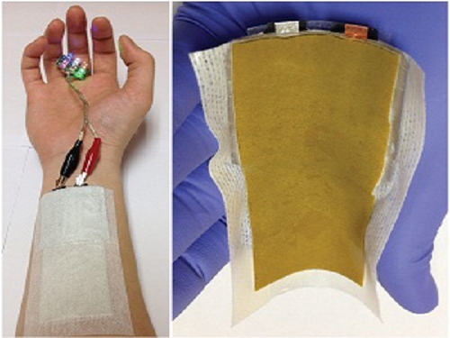 KAIST Develops a Credit-Card-Thick Flexible Lithium Ion Battery
Since the battery can be charged wirelessly, useful applications are expected including medical patches and smart cards.
Professor Jang Wook Choi at KAIST’s Graduate School of Energy, Environment, Water, and Sustainability (EEWS) and Dr. Jae Yong Song at the Korea Research Institute of Standards and Science jointly led research to invent a flexible lithium ion battery that is thinner than a credit card and can be charged wirelessly.
Their research findings were published online in Nano Letters on March 6, 2015. Lithium ion batteries are widely used today in various electronics including mobile devices and electronic cars. Researchers said that their work could help accelerate the development of flexible and wearable electronics.
Conventional lithium ion batteries are manufactured based on a layering technology, stacking up anodes, separating films, and cathodes like a sandwich, which makes it difficult to reduce their thickness. In addition, friction arises between layers, making the batteries impossible to bend. The coating films of electrodes easily come off, which contributes to the batteries’ poor performance.
The research team abandoned the existing production technology. Instead, they removed the separating films, layered the cathodes and anodes collinearly on a plane, and created a partition between electrodes to eliminate potential problems, such as short circuits and voltage dips, commonly present in lithium ion batteries.
After more than five thousand consecutive flexing experiments, the research team confirmed the possibility of a more flexible electrode structure while maintaining the battery performance comparable to the level of current lithium ion batteries.
Flexible batteries can be applied to integrated smart cards, cosmetic and medical patches, and skin adhesive sensors that can control a computer with voice commands or gesture as seen in the movie “Iron Man.”
Moreover, the team has successfully developed wireless-charging technology using electromagnetic induction and solar batteries.
They are currently developing a mass production process to combine this planar battery technology and printing, to ultimately create a new paradigm to print semiconductors and batteries using 3D printers.
Professor Choi said, “This new technology will contribute to diversifying patch functions as it is applicable to power various adhesive medical patches.”
Picture 1: Medical patch (left) and flexible secondary battery (right)
Picture 2: Diagram of flexible battery
Picture 3: Smart card embedding flexible battery
2015.03.24 View 12869
 -
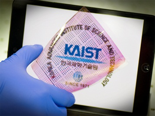 KAIST Develops Ultrathin Polymer Insulators Key to Low-Power Soft Electronics
Using an initiated chemical vapor deposition technique, the research team created an ultrathin polymeric insulating layer essential in realizing transistors with flexibility and low power consumption. This advance is expected to accelerate the commercialization of wearable and soft electronics.
A group of researchers at the Korea Advanced Institute of Science and Technology (KAIST) developed a high-performance ultrathin polymeric insulator for field-effect transistors (FETs). The researchers used vaporized monomers to form polymeric films grown conformally on various surfaces including plastics to produce a versatile insulator that meets a wide range of requirements for next-generation electronic devices. Their research results were published online in Nature Materials on March 9th, 2015.
FETs are an essential component for any modern electronic device used in our daily life from cell phones and computers, to flat-panel displays. Along with three electrodes (gate, source, and drain), FETs consist of an insulating layer and a semiconductor channel layer. The insulator in FETs plays an important role in controlling the conductance of the semiconductor channel and thus current flow within the translators. For reliable and low-power operation of FETs, electrically robust, ultrathin insulators are essential. Conventionally, such insulators are made of inorganic materials (e.g., oxides and nitrides) built on a hard surface such as silicon or glass due to their excellent insulating performance and reliability.
However, these insulators were difficult to implement into soft electronics due to their rigidity and high process temperature. In recent years, many researchers have studied polymers as promising insulating materials that are compatible with soft unconventional substrates and emerging semiconductor materials. The traditional technique employed in developing a polymer insulator, however, had the limitations of low surface coverage at ultra-low thickness, hindering FETs adopting polymeric insulators from operating at low voltage.
A KAIST research team led by Professor Sung Gap Im of the Chemical and Biomolecular Engineering Department and Professor Seunghyup Yoo and Professor Byung Jin Cho of the Electrical Engineering Department developed an insulating layer of organic polymers, “pV3D3,” that can be greatly scaled down, without losing its ideal insulating properties, to a thickness of less than 10 nanometers (nm) using the all-dry vapor-phase technique called the “initiated chemical vapor deposition (iCVD).”
The iCVD process allows gaseous monomers and initiators to react with each other in a low vacuum condition, and as a result, conformal polymeric films with excellent insulating properties are deposited on a substrate. Unlike the traditional technique, the surface-growing character of iCVD can overcome the problems associated with surface tension and produce highly uniform and pure ultrathin polymeric films over a large area with virtually no surface or substrate limitations. Furthermore, most iCVD polymers are created at room temperature, which lessens the strain exerted upon and damage done to the substrates.
With the pV3D3 insulator, the research team built low-power, high-performance FETs based on various semiconductor materials such as organics, graphene, and oxides, demonstrating the pV3D3 insulator’s wide range of material compatibility. They also manufactured a stick-on, removable electronic component using conventional packaging tape as a substrate. In collaboration with Professor Yong-Young Noh from Dongguk University in Korea, the team successfully developed a transistor array on a large-scale flexible substrate with the pV3D3 insulator.
Professor Im said, “The down-scalability and wide range of compatibility observed with iCVD-grown pV3D3 are unprecedented for polymeric insulators. Our iCVD pV3D3 polymeric films showed an insulating performance comparable to that of inorganic insulating layers, even when their thickness were scaled down to sub-10 nm. We expect our development will greatly benefit flexible or soft electronics, which will play a key role in the success of emerging electronic devices such as wearable computers.”
The title of the research paper is “Synthesis of ultrathin polymer insulating layers by initiated chemical vapor deposition for low-power soft electronics” (Digital Object Identifier (DOI) number is 10.1038/nmat4237).
Picture 1: A schematic image to show how the initiated chemical vapor deposition (iCVD) technique produces pV3D3 polymeric films: (i) introduction of vaporized monomers and initiators, (ii) activation of initiators to thermally dissociate into radicals, (iii) adsorption of monomers and initiator radicals onto a substrate, and (iv) transformation of free-radical polymerization into pV3D3 thin films.
Picture 2: This is a transistor array fabricated on a large scale, highly flexible substrate with pV3D3 polymeric films.
Picture 3: This photograph shows an electronic component fabricated on a conventional packaging tape, which is attachable or detachable, with pV3D3 polymeric films embedded.
2015.03.10 View 13784
 -
 News Article: Flexible, High-performance Nonvolatile Memory Developed with SONOS Technology
Professor Yang-Kyu Choi of KAIST’s Department of Electrical Engineering and his team presented a research paper entitled “Flexible High-performance Nonvolatile Memory by Transferring GAA Silicon Nanowire SONOS onto a Plastic Substrate” at the conference of the International Electron Devices Meeting that took place on December 15-17, 2014 in San Francisco.
The Electronic Engineering Journal (http://www.eejournal.com/) recently posted an article on the paper:
Electronic Engineering Journal, February 2, 2015
“A Flat-Earth Memory”
Another Way to Make the Brittle Flexible
http://www.techfocusmedia.net/archives/articles/20150202-flexiblegaa/?printView=true
2015.02.03 View 7999
 -
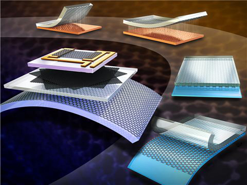 KAIST Develops a Method to Transfer Graphene by Stamping
Professor Sung-Yool Choi’s research team from KAIST's Department of Electrical Engineering has developed a technique that can produce a single-layer graphene from a metal etching. Through this, transferring a graphene layer onto a circuit board can be done as easily as stamping a seal on paper.
The research findings were published in the January 14th issue of Small as the lead article.
This technology will allow different types of wafer transfer methods such as transfer onto a surface of a device or a curved surface, and large surface transfer onto a 4 inch wafer. It will be applied in the field of wearable smart gadgets through commercialization of graphene electronic devices.
The traditional method used to transfer graphene onto a circuit board is a wet transfer. However, it has some drawbacks as the graphene layer can be damaged or contaminated during the transfer process from residue from the metal etching. This may affect the electrical properties of the transferred graphene.
After a graphene growth substrate formed on a catalytic metal substrate is pretreated in an aqueous poly vinyl alcohol (PVA) solution, a PVA film forms on the pretreated substrate. The substrate and the graphene layers bond strongly. The graphene is lifted from the growth substrate by means of an elastomeric stamp.
The delaminated graphene layer is isolated state from the elastomeric stamp and thus can be freely transferred onto a circuit board. As the catalytic metal substrate can be reused and does not contain harmful chemical substances, such transfer method is very eco-friendly.
Professor Choi said, “As the new graphene transfer method has a wide range of applications and allows a large surface transfer, it will contribute to the commercialization of graphene electronic devices.” He added that “because this technique has a high degree of freedom in transfer process, it has a variety of usages for graphene and 2 dimensional nano-devices.”
This research was sponsored by the Ministry of Science, ICT and Future Planning, the Republic of Korea.
Figure 1. Cover photo of the journal Small which illustrates the research findings
Figure 2. Above view of Graphene layer transferred through the new method
Figure 3. Large surface transfer of Graphene
2015.01.23 View 11647
 -
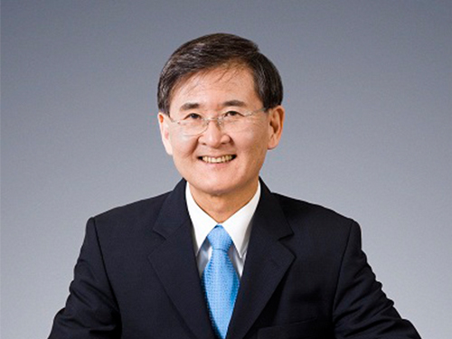 President Steve Kang will serve as the Chairman of Global Agenda Council on the Future of Electronics of the World Economic Forum
President Steve Kang of KAIST has been appointed to the Chairman of the Global Agenda Council (GAC) on the Future of Electronics of the World Economic Forum (WEF). He will serve the position for two years until September 2016.
President Kang and WEF council members co-hosted, with the government of the United Arab Emirates (UAE), the Future Circles Initiative, a future-focused, innovative brainstorming conference to help find strategies and ideas for the development of UAE. The conference took place on November 11-12, 2014 at the Mina Al Salam Hotel in Dubai.
WEF has about 80 GACs. Each council consists of 15 experts and thought leaders from the academia, industry, government, business, and non-profit sector and deals with specific issues that are important and relevant to the global community such as ageing, artificial intelligence and robotics, brain research, food and nutrition security, education, social media, and future of chemicals, advanced materials and biotechnology.
President Kang was recognized for his contribution to the advancement of science and higher education as an engineer, scholar, and professor. He led the development of the world’s premier CMOS 32-bit microprocessors while working at the AT&T Bell Laboratories. He also taught and conducted research at the University of California, Santa Cruz, and the University of Illinois, Urbana-Champaign. President Kang served as the chancellor of the University of California at Merced from March 2007 to June 2011.
2014.11.11 View 9653
 -
 KAIST Registers an Internationally Recognized Standard Patent
A video compression technology, jointly developed by Professor Mun-Chul Kim of the Department of Electrical Engineering at KAIST, the Electronics and Telecommunications Research Institute (ETRI), and the Korean Broadcasting System (KBS), is registered internationally as the standard patent in the next-generation High Efficiency Video Coding (HEVC).
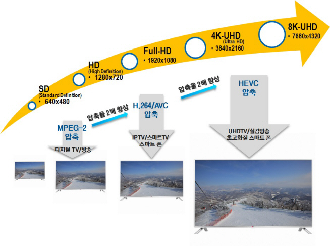
HEVC (H.265) is an international technology standard that compresses large image data for Ultra High Definition (UHD) televisions and smartphones. It has the twice the compression efficiency as that of H.264/AVC which is most commonly used for processing full HD sources. This means that it is able to compress a video file to half the size while maintaining the same image quality.
Although the related market is at a nascent stage, HEVC technology has already been applied to the latest version of televisions and smartphones. Experts predict that the market will grow to USD 200 billion by 2016, and KAIST is expected to receive a royalty payment of USD 9.3 million from this patent.
The International Organization for Standardization (ISO/IEC) established the HEVC standard in January 2013. Also, an international patent pool licensing corporation, MPEG LA announced the HEVC standard patent pool on September 29, 2014.
Professor Joongmyeon Bae, Dean of the Office of University-Industry Cooperation (OUIC) of KAIST, said, “This is an unprecedented case for Korea whereby a core technology developed by a university became an international standard, which has a vast impact on the market.”
President of KAIST, Steve Kang commented, “With its advanced technology, KAIST joined the HEVC standard patent pool as one of the 23 founding members along with Apple, Siemens, and NEC. This is a remarkable achievement.”
Picture 1: Improvements in video compression technology
Picture 2: Comparison of different screen resolutions
2014.10.09 View 13277
 -
 KAIST Co-owns the HEVC Patent Portfolio License
MPEG LA, LLC, a firm based in Denver, Colorado, which licenses patent pools covering essential patents required for the use of video coding technology, such as MPEG-2, MPEG-4 Visual (Part 2), and HEVC/H.264, announced the availability of the High Efficiency Video Coding (HEVC) Patent Portfolio License on September 29, 2014.
The HEVC standard, also known as H.265 and MPEG-H Part 2, is necessary to improve video coding and transmission efficiency for the Internet, televisions, and mobile gadgets with increased speed and capacity.
Through the portfolio license, users can easily obtain patent rights required for the HEVC standard in a single transaction, instead of negotiating separate licenses from multiple patent holders.
A total of 23 enterprises currently own essential HEVC patents. KAIST is the only Korean university among the joint patent owners. Collaborating with the Korea Broadcasting System (KBS) and the Electronics and Telecommunications Research Institute (ETRI), Professor Mun-Chul Kim of the Electrical Engineering Department at KAIST developed one of the core patents.
For a link to a press release distributed by MPEG LA, LLC, please see:
MPEG LA, LLC, September 29, 2014
"MPEG LA, LLC Offers HEVC Patent Portfolio License"
http://www.mpegla.com/main/Pages/Media.aspx
2014.10.02 View 13634
 -
 Extracting Light from Graphite: Core Technology of Graphene Quantum Dots Display Developed
Professor Seokwoo Jeon of the Department of Materials Science and Engineering, Professor Yong-Hoon Cho of the Department of Physics, and Professor Seunghyup Yoo of the Department of Electrical Engineering announced that they were able to develop topnotch graphene quantum dots from graphite.
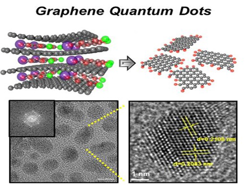
Using the method of synthesizing graphite intercalation compound from graphite with salt and water, the research team developed graphene quantum dots in an ecofriendly way.
The quantum dots have a diameter of 5 nanometers with their sizes equal and yield high quantum efficiency. Unlike conventional quantum dots, they are not comprised of toxic materials such as lead or cadmium. As the quantum dots can be developed from materials which can be easily found in the nature, researchers look forward to putting these into mass production at low cost.
The research team also discovered a luminescence mechanism of graphene quantum dots and confirmed the possibility of commercial use by developing quantum dot light-emitting diodes with brightness of 1,000 cd/m2, which is greater than that of cellphone displays.
Professor Seokwoo Jeon said, “Although quantum dot LEDs have a lower luminous efficiency than existing ones, their luminescent property can be further improved” and emphasized that “using quantum dot displays will allow us to develop not only paper-thin displays but also flexible ones.”
Sponsored by Graphene Research Center in KAIST Institute for NanoCentury, the research finding was published online in the April 20th issue of Advanced Optical Materials.
Picture 1: Graphene quantum dots and their synthesis
Picture 2: Luminescence mechanism of graphene quantum dots
Picture 3: Structure of graphene quantum dots LED and its emission
2014.09.06 View 18407