res
-
 KAIST Presents the Largest Number of Research Papers at the 2015 ISSCC
KAIST will present the largest number of research papers at the 2015 IEEE International Solid-State Circuits Conference (ISSCC), a leading global forum held every year to share professional knowledge and advancements in solid-state circuits and systems-on-a-chip. The Institute of Electrical and Electronics Engineers (IEEE) Solid-State Circuits Society sponsors the conference.
This year, the conference accepted 13 research papers from KAIST, ranking first among the participating organizations. Samsung Electronics Co., Ltd. took second (9 papers) place, and Intel Corporation and IMEC were in third place with 8 papers, respectively. A total of 610 papers were submitted, and reviewers selected only 206 papers for presentation at the next year's conference.
Since 2011, KAIST has been the number one institution among universities with the largest number of papers presented at the conference.
The Associate Chair of ISSCC Program Committee Chair, Professor Hoi-Jun Yoo of the Department of Electrical Engineering at KAIST, said, “Korea started the semiconductor industry in the 1970s, and since then, KAIST has been the center of research and development for the industry. With the establishment of IC (integrated circuit) Design Education Center in 1995, KAIST has contributed tremendously to the education and research of semiconductor production, nationally and globally. As shown from the record of presenting research results at the ISSCC, KAIST will continue to collaborate closely with the industry and lead the field.”
The 2015 IEEE ISSCC will take place on February 22-26, 2015 in San Francisco, CA, in the US.
2014.12.08 View 8664
KAIST Presents the Largest Number of Research Papers at the 2015 ISSCC
KAIST will present the largest number of research papers at the 2015 IEEE International Solid-State Circuits Conference (ISSCC), a leading global forum held every year to share professional knowledge and advancements in solid-state circuits and systems-on-a-chip. The Institute of Electrical and Electronics Engineers (IEEE) Solid-State Circuits Society sponsors the conference.
This year, the conference accepted 13 research papers from KAIST, ranking first among the participating organizations. Samsung Electronics Co., Ltd. took second (9 papers) place, and Intel Corporation and IMEC were in third place with 8 papers, respectively. A total of 610 papers were submitted, and reviewers selected only 206 papers for presentation at the next year's conference.
Since 2011, KAIST has been the number one institution among universities with the largest number of papers presented at the conference.
The Associate Chair of ISSCC Program Committee Chair, Professor Hoi-Jun Yoo of the Department of Electrical Engineering at KAIST, said, “Korea started the semiconductor industry in the 1970s, and since then, KAIST has been the center of research and development for the industry. With the establishment of IC (integrated circuit) Design Education Center in 1995, KAIST has contributed tremendously to the education and research of semiconductor production, nationally and globally. As shown from the record of presenting research results at the ISSCC, KAIST will continue to collaborate closely with the industry and lead the field.”
The 2015 IEEE ISSCC will take place on February 22-26, 2015 in San Francisco, CA, in the US.
2014.12.08 View 8664 -
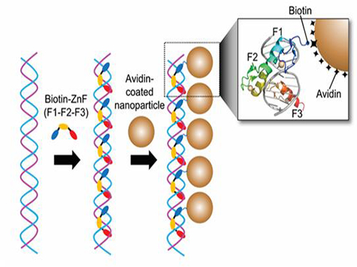 Nanoparticle Cluster Manufacturing Technique Using DNA Binding Protein Developed
Professor Hak-Sung Kim of the Department of Biological Sciences at KAIST and Yiseul Ryu, a doctoral candidate, used the Zinc Finger protein that specifically binds to target DNA sequence to develop a new manufacturing technique for size-controllable magnetic Nanoparticle Clusters (NPCs). Their research results were published in Angewandte Chemie International Edition online on 25 November 2014.
NPCs are structures consisting of magnetic nanoparticles, gold nanoparticles, and quantum dots, each of which are smaller than 100 nm (10-9m). NPCs have a distinctive property of collectivity not seen in single nanoparticles.
Specifically NPCS differ in physical and optical properties such as Plasmon coupling absorbance, energy transfers between particles, electron transfers, and conductivity. Therefore, NPCs can be employed in biological and medical research as well as the development of nanoelectric and nanoplasmon devices.
To make use of these novel properties, the size and the composition of the cluster must be exquisitely controlled. However, previous techniques relied on chemical binding which required complex steps, making it difficult to control the size and composition of NPCs.
Professor Kim’s team used Zinc Finger, a DNA binding protein, to develop a NPCs manufacturing technique to create clusters of the desired size easily. The Zinc Finger protein contains a zinc ion and specifically recognizes DNA sequence upon binding, which allows the exquisite control of the size and the cluster composition. The technique is also bio-friendly.
Professor Kim’s team created linear structure of different sizes of NPCs using Zinc Finger proteins and three DNA sequences of different lengths. The NPCs they produced confirmed their ability to control the size and structure of the cluster by using different DNA lengths.
The NPCs showed tripled T2 relaxation rates compared to the existing MRI contrast media (Feridex) and effectively transported to targeted cells. The research findings show the potential use of NPCs in biological and medical fields such as MRI contrast media, fluorescence imaging, and drug transport.
The research used the specific binding property of protein and DNA to develop a new method to create an inorganic nanoparticle’s supramolecular assembly. The technique can be used and applied extensively in other nanoparticles for future research in diagnosis, imaging, and drug and gene delivery.
Figure 1. A Mimetic Diagram of NPCs Manufacturing Technique Using DNA Binding Protein Zinc Finger
Figure 2. Transmission Electron Microscopy Images showing different sizes of NPCs depending on the length of the DNA
2014.12.04 View 13759
Nanoparticle Cluster Manufacturing Technique Using DNA Binding Protein Developed
Professor Hak-Sung Kim of the Department of Biological Sciences at KAIST and Yiseul Ryu, a doctoral candidate, used the Zinc Finger protein that specifically binds to target DNA sequence to develop a new manufacturing technique for size-controllable magnetic Nanoparticle Clusters (NPCs). Their research results were published in Angewandte Chemie International Edition online on 25 November 2014.
NPCs are structures consisting of magnetic nanoparticles, gold nanoparticles, and quantum dots, each of which are smaller than 100 nm (10-9m). NPCs have a distinctive property of collectivity not seen in single nanoparticles.
Specifically NPCS differ in physical and optical properties such as Plasmon coupling absorbance, energy transfers between particles, electron transfers, and conductivity. Therefore, NPCs can be employed in biological and medical research as well as the development of nanoelectric and nanoplasmon devices.
To make use of these novel properties, the size and the composition of the cluster must be exquisitely controlled. However, previous techniques relied on chemical binding which required complex steps, making it difficult to control the size and composition of NPCs.
Professor Kim’s team used Zinc Finger, a DNA binding protein, to develop a NPCs manufacturing technique to create clusters of the desired size easily. The Zinc Finger protein contains a zinc ion and specifically recognizes DNA sequence upon binding, which allows the exquisite control of the size and the cluster composition. The technique is also bio-friendly.
Professor Kim’s team created linear structure of different sizes of NPCs using Zinc Finger proteins and three DNA sequences of different lengths. The NPCs they produced confirmed their ability to control the size and structure of the cluster by using different DNA lengths.
The NPCs showed tripled T2 relaxation rates compared to the existing MRI contrast media (Feridex) and effectively transported to targeted cells. The research findings show the potential use of NPCs in biological and medical fields such as MRI contrast media, fluorescence imaging, and drug transport.
The research used the specific binding property of protein and DNA to develop a new method to create an inorganic nanoparticle’s supramolecular assembly. The technique can be used and applied extensively in other nanoparticles for future research in diagnosis, imaging, and drug and gene delivery.
Figure 1. A Mimetic Diagram of NPCs Manufacturing Technique Using DNA Binding Protein Zinc Finger
Figure 2. Transmission Electron Microscopy Images showing different sizes of NPCs depending on the length of the DNA
2014.12.04 View 13759 -
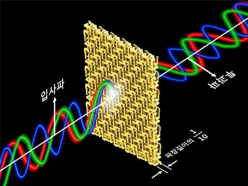 Broadband and Ultrathin Polarization Manipulators Developed
Professor Bumki Min from the Department of Mechanical Engineering at KAIST has developed a technology that can manipulate a polarized light in broadband operation with the use of a metamaterial.
It is expected that this technology will lead to the development of broadband optical devices that can be applied to broadband communication and display.
When an object or its structure is analyzed by using a polarized light such as a laser, the results are generally affected by the polarized state of the light. Therefore, in an optics laboratory, the light is polarized by various methods.
In such cases, researchers employ wave plates or photoactive materials. However, the performance of these devices depend vastly on wavelength, and so they are not suitable to be used as a polarizer, especially in broadband.
There were many attempts to make artificial materials that are very photoactive by using metamaterials which have a strong resonance. Nonetheless, because the materials had an unavoidable dispersion in the resonance frequency, they were not adequate for broadband operation.
Professor Min’s research team arranged and connected helical metamaterials that are smaller than the wavelength of light. They verified theoretically and experimentally that polarized light can be constantly rotated regardless of the wavelength by super-thin materials that have thickness less than one-tenth of the wavelength of the light. The experiment which confirmed the theory was conducted in the microwave band.
Broadband polarized rotational 3D metamaterials were found to rotate the polarized microwave within the range of 0.1 GHz to 40 GHz by 45 degrees regardless of its frequency. This nondispersive property is quite unnatural because it is difficult to find a material that does not change in a wide band.
In addition, the research team materialized the broadband nondispersive polarized rotational property by designing the metamaterial in a way that it has chirality, which determines the number of rotations proportional to the wavelength.
Professor Min said, “As the technology is able to manipulate ultrathin polarization of light in broadband, it will lead to the creation of ultra-shallow broadband optical devices.”
Sponsored by the Ministry of Science, ICT and Future Planning of the Republic of Korea and the National Research Foundation of Korea, this research was led by a PhD candidate, Hyun-Sung Park, under the guidance of Professor Min. The research findings were published online in the November 17th issue of Nature Communications.
Figure 1 – Broadband and Ultrathin Polarization Manipulators Produced by 3D Printer
Figure 2 – Concept of Broadband and Ultrathin Polarization Manipulators
2014.12.03 View 12266
Broadband and Ultrathin Polarization Manipulators Developed
Professor Bumki Min from the Department of Mechanical Engineering at KAIST has developed a technology that can manipulate a polarized light in broadband operation with the use of a metamaterial.
It is expected that this technology will lead to the development of broadband optical devices that can be applied to broadband communication and display.
When an object or its structure is analyzed by using a polarized light such as a laser, the results are generally affected by the polarized state of the light. Therefore, in an optics laboratory, the light is polarized by various methods.
In such cases, researchers employ wave plates or photoactive materials. However, the performance of these devices depend vastly on wavelength, and so they are not suitable to be used as a polarizer, especially in broadband.
There were many attempts to make artificial materials that are very photoactive by using metamaterials which have a strong resonance. Nonetheless, because the materials had an unavoidable dispersion in the resonance frequency, they were not adequate for broadband operation.
Professor Min’s research team arranged and connected helical metamaterials that are smaller than the wavelength of light. They verified theoretically and experimentally that polarized light can be constantly rotated regardless of the wavelength by super-thin materials that have thickness less than one-tenth of the wavelength of the light. The experiment which confirmed the theory was conducted in the microwave band.
Broadband polarized rotational 3D metamaterials were found to rotate the polarized microwave within the range of 0.1 GHz to 40 GHz by 45 degrees regardless of its frequency. This nondispersive property is quite unnatural because it is difficult to find a material that does not change in a wide band.
In addition, the research team materialized the broadband nondispersive polarized rotational property by designing the metamaterial in a way that it has chirality, which determines the number of rotations proportional to the wavelength.
Professor Min said, “As the technology is able to manipulate ultrathin polarization of light in broadband, it will lead to the creation of ultra-shallow broadband optical devices.”
Sponsored by the Ministry of Science, ICT and Future Planning of the Republic of Korea and the National Research Foundation of Korea, this research was led by a PhD candidate, Hyun-Sung Park, under the guidance of Professor Min. The research findings were published online in the November 17th issue of Nature Communications.
Figure 1 – Broadband and Ultrathin Polarization Manipulators Produced by 3D Printer
Figure 2 – Concept of Broadband and Ultrathin Polarization Manipulators
2014.12.03 View 12266 -
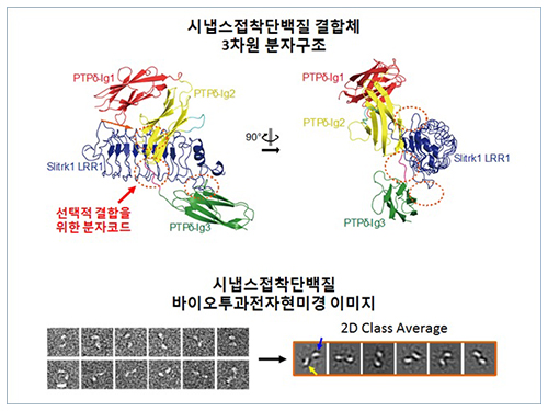 Structure of Neuron-Connecting Synaptic Adhesion Molecules Discovered
A research team has found the three-dimensional structure of synaptic adhesion molecules, which orchestrate synaptogenesis. The research findings also propose the mechanism of synapses in its initial formation. Some brain diseases such as obsessive compulsive disorder (OCD) or bipolar disorders arise from a malfunction of synapses. The team expects the findings to be applied in investigating pathogenesis and developing medicines for such diseases.
The research was conducted by a Master’s candidate Kee Hun Kim, Professor Ji Won Um from Yonsei University, and Professor Beom Seok Park from Eulji University under the guidance of Professor Homin Kim from the Graduate School of Medical Science and Engineering, KAIST, and Professor Jaewon Ko from Yonsei University. Sponsored by the Ministry of Science, ICT and Future Planning and the National Research Foundation of Korea, the research findings were published online in the November 14th issue of Nature Communications.
A protein that exists in the neuronal transmembrane, Slitrk, interacts with the presynaptic leukocyte common antigen-related receptor protein tyrosine phosphatases (LAR-RPTPs) and forms a protein complex. It is involved in the development of synapses in the initial stage, and balances excitatory and inhibitory signals of neurons.
It is known that a disorder in those two proteins cause a malfunction of synapses, resulting in neuropsychosis such as autism, epilepsy, OCD, and bipolar disorders. However, because the structure as well as synaptogenic function of these proteins were not understood, the development of cures could not progress.
The research team discovered the three-dimensional structure of two synaptic adhesion molecules like Slitrk and LAR-RPTPs and identified the regions of interaction through protein crystallography and transmission electron microscopy (TEM). Furthermore, they found that the formation of the synapse is induced after the combination of two synaptic adhesion molecules develops a cluster.
Professor Kim said, “The research findings will serve as a basis of understanding the pathogenesis of brain diseases which arises from a malfunction of synaptic adhesion molecules. In particular, this is a good example in which collaboration between structural biology and neurobiology has led to a fruitful result.” Professor Ko commented that “this will give new directions to synaptic formation-related-researches by revealing the molecular mechanism of synaptic adhesion molecules.”
Figure 1: Overview of the PTPd Ig1–3/Slitrk1 LRR1 complex.
Figure 2: Representative negative-stained electron microscopy images of Slitrk1 Full ectodomain (yellow arrows indicate the horseshoe-shaped LRR domains). The typical horseshoe-shaped structures and the randomness of the relative positions of each LRR domain can be observed from the two-dimensional class averages displayed in the orange box.
Figure 3: Model of the two-step presynaptic differentiation process mediated by the biding of Slitrks to LAR-RPTPs and subsequent lateral assembly of trans-synaptic LAR-RPTPs/Slitrik complexes.
2014.11.28 View 12600
Structure of Neuron-Connecting Synaptic Adhesion Molecules Discovered
A research team has found the three-dimensional structure of synaptic adhesion molecules, which orchestrate synaptogenesis. The research findings also propose the mechanism of synapses in its initial formation. Some brain diseases such as obsessive compulsive disorder (OCD) or bipolar disorders arise from a malfunction of synapses. The team expects the findings to be applied in investigating pathogenesis and developing medicines for such diseases.
The research was conducted by a Master’s candidate Kee Hun Kim, Professor Ji Won Um from Yonsei University, and Professor Beom Seok Park from Eulji University under the guidance of Professor Homin Kim from the Graduate School of Medical Science and Engineering, KAIST, and Professor Jaewon Ko from Yonsei University. Sponsored by the Ministry of Science, ICT and Future Planning and the National Research Foundation of Korea, the research findings were published online in the November 14th issue of Nature Communications.
A protein that exists in the neuronal transmembrane, Slitrk, interacts with the presynaptic leukocyte common antigen-related receptor protein tyrosine phosphatases (LAR-RPTPs) and forms a protein complex. It is involved in the development of synapses in the initial stage, and balances excitatory and inhibitory signals of neurons.
It is known that a disorder in those two proteins cause a malfunction of synapses, resulting in neuropsychosis such as autism, epilepsy, OCD, and bipolar disorders. However, because the structure as well as synaptogenic function of these proteins were not understood, the development of cures could not progress.
The research team discovered the three-dimensional structure of two synaptic adhesion molecules like Slitrk and LAR-RPTPs and identified the regions of interaction through protein crystallography and transmission electron microscopy (TEM). Furthermore, they found that the formation of the synapse is induced after the combination of two synaptic adhesion molecules develops a cluster.
Professor Kim said, “The research findings will serve as a basis of understanding the pathogenesis of brain diseases which arises from a malfunction of synaptic adhesion molecules. In particular, this is a good example in which collaboration between structural biology and neurobiology has led to a fruitful result.” Professor Ko commented that “this will give new directions to synaptic formation-related-researches by revealing the molecular mechanism of synaptic adhesion molecules.”
Figure 1: Overview of the PTPd Ig1–3/Slitrk1 LRR1 complex.
Figure 2: Representative negative-stained electron microscopy images of Slitrk1 Full ectodomain (yellow arrows indicate the horseshoe-shaped LRR domains). The typical horseshoe-shaped structures and the randomness of the relative positions of each LRR domain can be observed from the two-dimensional class averages displayed in the orange box.
Figure 3: Model of the two-step presynaptic differentiation process mediated by the biding of Slitrks to LAR-RPTPs and subsequent lateral assembly of trans-synaptic LAR-RPTPs/Slitrik complexes.
2014.11.28 View 12600 -
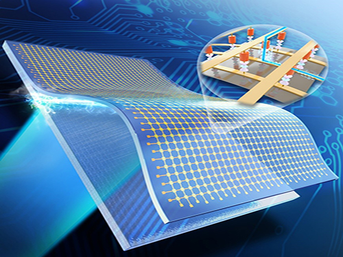 Breakthrough in Flexible Electronics Enabled by Inorganic-based Laser Lift-off
Flexible electronics have been touted as the next generation in electronics in various areas, ranging from consumer electronics to bio-integrated medical devices. In spite of their merits, insufficient performance of organic materials arising from inherent material properties and processing limitations in scalability have posed big challenges to developing all-in-one flexible electronics systems in which display, processor, memory, and energy devices are integrated. The high temperature processes, essential for high performance electronic devices, have severely restricted the development of flexible electronics because of the fundamental thermal instabilities of polymer materials.
A research team headed by Professor Keon Jae Lee of the Department of Materials Science and Engineering at KAIST provides an easier methodology to realize high performance flexible electronics by using the Inorganic-based Laser Lift-off (ILLO).
The ILLO process involves depositing a laser-reactive exfoliation layer on rigid substrates, and then fabricating ultrathin inorganic electronic devices, e.g., high density crossbar memristive memory on top of the exfoliation layer. By laser irradiation through the back of the substrate, only the ultrathin inorganic device layers are exfoliated from the substrate as a result of the reaction between laser and exfoliation layer, and then subsequently transferred onto any kind of receiver substrate such as plastic, paper, and even fabric.
This ILLO process can enable not only nanoscale processes for high density flexible devices but also the high temperature process that was previously difficult to achieve on plastic substrates. The transferred device successfully demonstrates fully-functional random access memory operation on flexible substrates even under severe bending.
Professor Lee said, “By selecting an optimized set of inorganic exfoliation layer and substrate, a nanoscale process at a high temperature of over 1000 °C can be utilized for high performance flexible electronics. The ILLO process can be applied to diverse flexible electronics, such as driving circuits for displays and inorganic-based energy devices such as battery, solar cell, and self-powered devices that require high temperature processes.”
The team’s results were published in the November issue of Wiley’s journal, ‘ Advanced Materials, ’ as a cover article entitled “ Flexible Crossbar-Structured Resistive Memory Arrays on Plastic Substrates via Inorganic-Based Laser Lift-Off.”
( http://onlinelibrary.wiley.com/doi/10.1002/adma.201402472/abstract )
This schematic picture shows the flexible crossbar memory developed via the ILLO process.
This photo shows the flexible RRAM device on a plastic substrate.
2014.11.26 View 10578
Breakthrough in Flexible Electronics Enabled by Inorganic-based Laser Lift-off
Flexible electronics have been touted as the next generation in electronics in various areas, ranging from consumer electronics to bio-integrated medical devices. In spite of their merits, insufficient performance of organic materials arising from inherent material properties and processing limitations in scalability have posed big challenges to developing all-in-one flexible electronics systems in which display, processor, memory, and energy devices are integrated. The high temperature processes, essential for high performance electronic devices, have severely restricted the development of flexible electronics because of the fundamental thermal instabilities of polymer materials.
A research team headed by Professor Keon Jae Lee of the Department of Materials Science and Engineering at KAIST provides an easier methodology to realize high performance flexible electronics by using the Inorganic-based Laser Lift-off (ILLO).
The ILLO process involves depositing a laser-reactive exfoliation layer on rigid substrates, and then fabricating ultrathin inorganic electronic devices, e.g., high density crossbar memristive memory on top of the exfoliation layer. By laser irradiation through the back of the substrate, only the ultrathin inorganic device layers are exfoliated from the substrate as a result of the reaction between laser and exfoliation layer, and then subsequently transferred onto any kind of receiver substrate such as plastic, paper, and even fabric.
This ILLO process can enable not only nanoscale processes for high density flexible devices but also the high temperature process that was previously difficult to achieve on plastic substrates. The transferred device successfully demonstrates fully-functional random access memory operation on flexible substrates even under severe bending.
Professor Lee said, “By selecting an optimized set of inorganic exfoliation layer and substrate, a nanoscale process at a high temperature of over 1000 °C can be utilized for high performance flexible electronics. The ILLO process can be applied to diverse flexible electronics, such as driving circuits for displays and inorganic-based energy devices such as battery, solar cell, and self-powered devices that require high temperature processes.”
The team’s results were published in the November issue of Wiley’s journal, ‘ Advanced Materials, ’ as a cover article entitled “ Flexible Crossbar-Structured Resistive Memory Arrays on Plastic Substrates via Inorganic-Based Laser Lift-Off.”
( http://onlinelibrary.wiley.com/doi/10.1002/adma.201402472/abstract )
This schematic picture shows the flexible crossbar memory developed via the ILLO process.
This photo shows the flexible RRAM device on a plastic substrate.
2014.11.26 View 10578 -
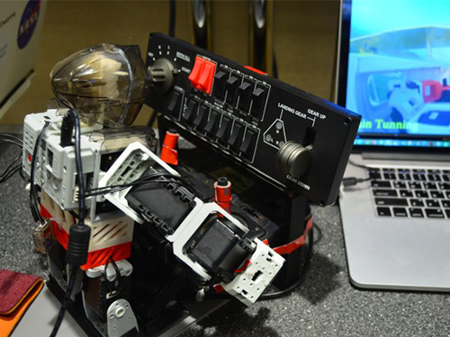
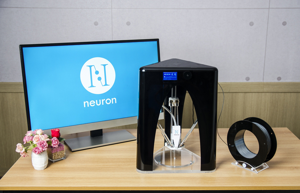 3D Printer Developed by KAIST Undergraduate Students
More than 100 Pre-orders Prior to Product Launch Made
KAIST undergraduate students received more than 100 pre-orders before the launch for 3D printers they developed and became a hot topic of interest.
KAIST Research Institute for Social Technology and Innovations (Head Hong-Kyu Lee) had a launch party at Daejeon Riviera Hotel on 17 November 2014 for “Commercial Delta 3D Printer” developed by KAIST undergraduate students inviting around 50 businesses, buyers and representatives of 3D Printing Industry Association.
“3D Printer” uses blueprints of products such as toys, mug cups and chairs to make 3D objects and is thought to be revolutionary technology in manufacturing industry. The interest has grown as recent printers could print even fruits and cosmetics.
The printing structure of 3D printer can be divided roughly into horizontal Mendel method and Delta method. KAIST students focused on the Delta method to give a differentiated product from 90% of commercial products that use Mendel method.
First, the students focused on lowering the cost of unit price by using self-developed components. The carriage (transport machine) of the product is replaced by self-developed components instead of bearing to reduce the noise and the linking method was changed to beads from loop guide to increase the completeness of the printed product. Also, an auto-levelling is loaded to ensure the nozzle and the bed is parallel and hence increasing convenience for the users. Further, the printer, designed by a product designer in Germany, is linked to a smartphone application for blueprints.
A student in the development team, Seokhyeon Seo (Department of Computer Science, 3rd Year Undergraduate) said, “The biggest merits of the product are lowering the price to a 1/3 by using self-developed components and reducing the noise.” He continued, “By using a smartphone application, anyone can easily design the product. So it is applicable to use for education or at home”
In the exhibit, “3D Printing Korea 2014,” in Coex, Seoul the printer had a preview demonstration, and received more than 100 pre-orders from educational and business training institutions. Further, buyers from Canada and the US requested opening agencies in their countries.
KAIST Research Institute for Social Technology and Innovations Head Hong-Kyu Lee said, “3D printing is an innovative technology that could bring the 3rd industrial revolution.” He continued, “It is still early days but the demand will increase exponentially.”
This project was a research project of KAIST Research Institute for Social Technology and Innovations led by a development team consisting of 4 undergraduate students of KAIST, one student from University of Oxford and one German product designer.
Students in the picture below are Won-Hoi Kim (Department of Mechanical Engineering), Sung-Hyun Cho (Department of Mechanical Engineering), and Suk-Hyun Seo (Department of Computer Science) from left to right.
2014.11.19 View 11550
3D Printer Developed by KAIST Undergraduate Students
More than 100 Pre-orders Prior to Product Launch Made
KAIST undergraduate students received more than 100 pre-orders before the launch for 3D printers they developed and became a hot topic of interest.
KAIST Research Institute for Social Technology and Innovations (Head Hong-Kyu Lee) had a launch party at Daejeon Riviera Hotel on 17 November 2014 for “Commercial Delta 3D Printer” developed by KAIST undergraduate students inviting around 50 businesses, buyers and representatives of 3D Printing Industry Association.
“3D Printer” uses blueprints of products such as toys, mug cups and chairs to make 3D objects and is thought to be revolutionary technology in manufacturing industry. The interest has grown as recent printers could print even fruits and cosmetics.
The printing structure of 3D printer can be divided roughly into horizontal Mendel method and Delta method. KAIST students focused on the Delta method to give a differentiated product from 90% of commercial products that use Mendel method.
First, the students focused on lowering the cost of unit price by using self-developed components. The carriage (transport machine) of the product is replaced by self-developed components instead of bearing to reduce the noise and the linking method was changed to beads from loop guide to increase the completeness of the printed product. Also, an auto-levelling is loaded to ensure the nozzle and the bed is parallel and hence increasing convenience for the users. Further, the printer, designed by a product designer in Germany, is linked to a smartphone application for blueprints.
A student in the development team, Seokhyeon Seo (Department of Computer Science, 3rd Year Undergraduate) said, “The biggest merits of the product are lowering the price to a 1/3 by using self-developed components and reducing the noise.” He continued, “By using a smartphone application, anyone can easily design the product. So it is applicable to use for education or at home”
In the exhibit, “3D Printing Korea 2014,” in Coex, Seoul the printer had a preview demonstration, and received more than 100 pre-orders from educational and business training institutions. Further, buyers from Canada and the US requested opening agencies in their countries.
KAIST Research Institute for Social Technology and Innovations Head Hong-Kyu Lee said, “3D printing is an innovative technology that could bring the 3rd industrial revolution.” He continued, “It is still early days but the demand will increase exponentially.”
This project was a research project of KAIST Research Institute for Social Technology and Innovations led by a development team consisting of 4 undergraduate students of KAIST, one student from University of Oxford and one German product designer.
Students in the picture below are Won-Hoi Kim (Department of Mechanical Engineering), Sung-Hyun Cho (Department of Mechanical Engineering), and Suk-Hyun Seo (Department of Computer Science) from left to right.
2014.11.19 View 11550 -
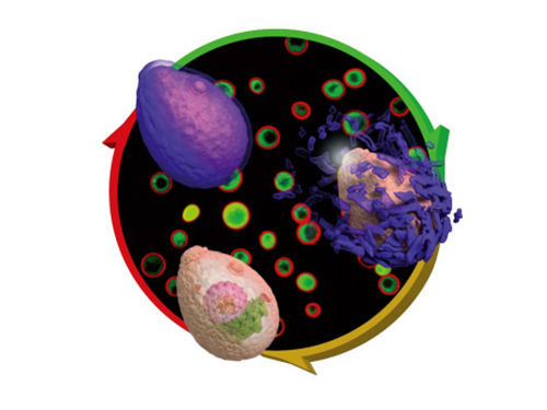 Eggshell-like Cell Encapsulation and Degradation Technology Developed
Some bacteria form endospores on cell walls to protect their DNA in case of nutrient deficiency. When an endospore meets a suitable environment for survival, the cell can revert to the original state from which it can reproduce.
The technique that can artificially control such phenomenon was developed by an international team of researchers. At first, a cell is wrapped and preserved like an egg. When the cell is needed, the technique allows the endospore to decompose while it is alive. Future applications for this technique include cell-based biosensor, cell therapy, and biocatalyst processes.
Professors Insung Choi and Younghoon Lee from the Department of Chemistry at KAIST as well as and Professor Frank Caruso from the University of Melbourne developed this technique which permits a cell to stay alive by coating it with film on a nanometer scale and then to be decomposed while it is alive.
The research finding was published in the November 10th issue of Angewandte Chemie International Edition as the lead article.
Cell encapsulation allows researchers to capture a cell in a tight capsule while it is alive. It is highly recognized in cell-based applications where the control of cell stability and cell-division is the biggest issue.
Traditional cell encapsulation methods utilized organic film or inorganic capsules that are made of organic film moldings. Although these films tightly closed around the cell, because they were not easily decomposable, it was difficult to apply the method.
The research team succeeded in encapsulating each cell in a metal-polyphenol film by mixing tannic acid and iron ion solution with yeast cells.
Usually extracted from oak barks or grape peels, tannic acid is a natural substance. It forms a metal-polyphenol film within ten seconds when it meets iron ions due to its high affinity with cells. Cells encapsulated with this film presented high survival rates. Since the film forms quickly in a simple manner, it was possible to obtain large amount of encapsulated cells.
The research team also found that the metal-polyphenol film was stable in neutral pH, but is easily degradable under a weak acidic condition. Using this property, they were able to control cell division by restoring the cell to its pre-encapsulated state at a desired moment.
Protecting the cell from the external environment like an egg shell, the metal-polyphenol film protected the cell against foreign conditions such as lytic enzymes, extended exposure to UV radiation, and silver nanoparticles. The research indicated that the encapsulated cells had a high survival rate even under extreme environments.
Professor Lee said that “not only the cells remain alive during the encapsulation stage, but also they can be protected under extreme environment.” He added, “This is an advanced cell encapsulation technology that allows controlling cell-division of those cells through responsive shell degradation on-demand.”
Professor Choi commented, “Although the cell encapsulation technology is still in its infancy, as the technology matures the application of cell-manipulation technology will be actualized.” He highlighted that “it will serve as a breakthrough to problems faced by cell-based applications.”
Sponsored by the Ministry of Science, ICT and Future Planning and the National Research Foundation of Korea, the research was led by two Master’s candidates, Ji Hun Park and Kyung Hwan Kim, under the joint guidance of research professors from KAIST and the University of Melbourne.
Figure 1: Lead article of Angewandte Chemie
Background: Shows a live native yeast (in green) encapsulated in a metal-polyphenol film (in red) illustrating the vitality of the yeast
Front: A native yeast at each encapsulation stage
Pictured on the bottom left is a cell prior to encapsulation. Following the red arrow, the native yeast is in purple to show metal-polyphenol film formed around the cell. The cell after the green arrow is a visualization of the degradation of the film in weak acidic condition.
Figure 2: A mimetic diagram of cell encapsulation with a metal-polyphenol film
Top: A native yeast before encapsulation
Middle: A native yeast encapsulated with Tannic Acid-Fe (III) Nanoshell – cell-division of the encapsulated cell is controlled by pH and the shell is protected against silver nanoparticle, lytic enzyme, and UV-C
Bottom: Shell degradation on-demand depending on pH
2014.11.18 View 10899
Eggshell-like Cell Encapsulation and Degradation Technology Developed
Some bacteria form endospores on cell walls to protect their DNA in case of nutrient deficiency. When an endospore meets a suitable environment for survival, the cell can revert to the original state from which it can reproduce.
The technique that can artificially control such phenomenon was developed by an international team of researchers. At first, a cell is wrapped and preserved like an egg. When the cell is needed, the technique allows the endospore to decompose while it is alive. Future applications for this technique include cell-based biosensor, cell therapy, and biocatalyst processes.
Professors Insung Choi and Younghoon Lee from the Department of Chemistry at KAIST as well as and Professor Frank Caruso from the University of Melbourne developed this technique which permits a cell to stay alive by coating it with film on a nanometer scale and then to be decomposed while it is alive.
The research finding was published in the November 10th issue of Angewandte Chemie International Edition as the lead article.
Cell encapsulation allows researchers to capture a cell in a tight capsule while it is alive. It is highly recognized in cell-based applications where the control of cell stability and cell-division is the biggest issue.
Traditional cell encapsulation methods utilized organic film or inorganic capsules that are made of organic film moldings. Although these films tightly closed around the cell, because they were not easily decomposable, it was difficult to apply the method.
The research team succeeded in encapsulating each cell in a metal-polyphenol film by mixing tannic acid and iron ion solution with yeast cells.
Usually extracted from oak barks or grape peels, tannic acid is a natural substance. It forms a metal-polyphenol film within ten seconds when it meets iron ions due to its high affinity with cells. Cells encapsulated with this film presented high survival rates. Since the film forms quickly in a simple manner, it was possible to obtain large amount of encapsulated cells.
The research team also found that the metal-polyphenol film was stable in neutral pH, but is easily degradable under a weak acidic condition. Using this property, they were able to control cell division by restoring the cell to its pre-encapsulated state at a desired moment.
Protecting the cell from the external environment like an egg shell, the metal-polyphenol film protected the cell against foreign conditions such as lytic enzymes, extended exposure to UV radiation, and silver nanoparticles. The research indicated that the encapsulated cells had a high survival rate even under extreme environments.
Professor Lee said that “not only the cells remain alive during the encapsulation stage, but also they can be protected under extreme environment.” He added, “This is an advanced cell encapsulation technology that allows controlling cell-division of those cells through responsive shell degradation on-demand.”
Professor Choi commented, “Although the cell encapsulation technology is still in its infancy, as the technology matures the application of cell-manipulation technology will be actualized.” He highlighted that “it will serve as a breakthrough to problems faced by cell-based applications.”
Sponsored by the Ministry of Science, ICT and Future Planning and the National Research Foundation of Korea, the research was led by two Master’s candidates, Ji Hun Park and Kyung Hwan Kim, under the joint guidance of research professors from KAIST and the University of Melbourne.
Figure 1: Lead article of Angewandte Chemie
Background: Shows a live native yeast (in green) encapsulated in a metal-polyphenol film (in red) illustrating the vitality of the yeast
Front: A native yeast at each encapsulation stage
Pictured on the bottom left is a cell prior to encapsulation. Following the red arrow, the native yeast is in purple to show metal-polyphenol film formed around the cell. The cell after the green arrow is a visualization of the degradation of the film in weak acidic condition.
Figure 2: A mimetic diagram of cell encapsulation with a metal-polyphenol film
Top: A native yeast before encapsulation
Middle: A native yeast encapsulated with Tannic Acid-Fe (III) Nanoshell – cell-division of the encapsulated cell is controlled by pH and the shell is protected against silver nanoparticle, lytic enzyme, and UV-C
Bottom: Shell degradation on-demand depending on pH
2014.11.18 View 10899 -
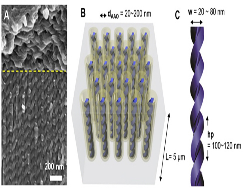 KAIST Develops Core Technology to Synthesize a Helical Nanostructure
Professor Dong-Ki Yoon’s research team of the Graduate School of Nanoscience and Technology (GSNT) at KAIST has developed helical nanostructures using self-assembly processes. The results were published in the Proceedings of the National Academy of Sciences of the United States of America(PNAS) on the October 7th.
This technology enables the synthesis of various helical structures on a relatively large confined area. Its synthesis is often considered the most arduous for three dimensional structures. Formed from liquid crystal, the structure holds a regular helical structure within the confined space of 20 to 300 nanometers. Also, the distance between each pattern increased as the diameter of the nanostructure increased.
Liquid crystals have a unique property of responding sensitively to the surrounding electromagnetic field. The technology, in combination with the electromagnetic property of liquid crystal, is expected to foster the development of highly efficient optoelectronic devices.
Using this technology, it is possible to develop three dimensional patterning technology beyond the current semiconductor manufacturing technology which uses two dimensional photolithography processes. Three-dimensional semiconductor devices are expected to store hundred times more data than current devices. They will also lower costs by simplifying manufacturing processes.
The essence of this research, “self-assembly in confined space,” refers to controlling complex nanostructures, which can be synthesized from materials such as macromolecules, liquid crystal molecules, and biomolecules in relation to surrounding environments including the temperature, concentration, and pH.
The research team produced a confined space with a length of tens of nanometers by using a porous anodized aluminum membrane induced from an electrochemical reaction. They successfully synthesized independently controlled helical nanostructures by forming the helical structures from liquid crystal molecules within that space.
Professor Yoon said, “This research examines the physicochemical principle of controlling helical nanostructures.” He highlighted the significance of the research and commented, “The technology enables the control of complex nanostructures from organic molecules by using confined space and surface reforming.”
He added that, “When grafted with nanotechnology or information technology, this technology will spur new growth to liquid crystal-related industries such as the LCD.”
The research was led by two Ph.D. candidates, Hanim Kim and Sunhee Lee, under the guidance of Professor Yoon. Dr. Tae-Joo Shin of the Pohang Accelerator Laboratory, Professor Sang-Bok Lee of the University of Maryland, and Professor Noel Clark of the University of Colorado also participated.
Picture 1. Electron Microscopy Pictures and Conceptual Diagrams of Helical Nanostructures
Picture 2. Electron Microscopy Pictures of Manufactured Helical Nanostructures
2014.10.29 View 9441
KAIST Develops Core Technology to Synthesize a Helical Nanostructure
Professor Dong-Ki Yoon’s research team of the Graduate School of Nanoscience and Technology (GSNT) at KAIST has developed helical nanostructures using self-assembly processes. The results were published in the Proceedings of the National Academy of Sciences of the United States of America(PNAS) on the October 7th.
This technology enables the synthesis of various helical structures on a relatively large confined area. Its synthesis is often considered the most arduous for three dimensional structures. Formed from liquid crystal, the structure holds a regular helical structure within the confined space of 20 to 300 nanometers. Also, the distance between each pattern increased as the diameter of the nanostructure increased.
Liquid crystals have a unique property of responding sensitively to the surrounding electromagnetic field. The technology, in combination with the electromagnetic property of liquid crystal, is expected to foster the development of highly efficient optoelectronic devices.
Using this technology, it is possible to develop three dimensional patterning technology beyond the current semiconductor manufacturing technology which uses two dimensional photolithography processes. Three-dimensional semiconductor devices are expected to store hundred times more data than current devices. They will also lower costs by simplifying manufacturing processes.
The essence of this research, “self-assembly in confined space,” refers to controlling complex nanostructures, which can be synthesized from materials such as macromolecules, liquid crystal molecules, and biomolecules in relation to surrounding environments including the temperature, concentration, and pH.
The research team produced a confined space with a length of tens of nanometers by using a porous anodized aluminum membrane induced from an electrochemical reaction. They successfully synthesized independently controlled helical nanostructures by forming the helical structures from liquid crystal molecules within that space.
Professor Yoon said, “This research examines the physicochemical principle of controlling helical nanostructures.” He highlighted the significance of the research and commented, “The technology enables the control of complex nanostructures from organic molecules by using confined space and surface reforming.”
He added that, “When grafted with nanotechnology or information technology, this technology will spur new growth to liquid crystal-related industries such as the LCD.”
The research was led by two Ph.D. candidates, Hanim Kim and Sunhee Lee, under the guidance of Professor Yoon. Dr. Tae-Joo Shin of the Pohang Accelerator Laboratory, Professor Sang-Bok Lee of the University of Maryland, and Professor Noel Clark of the University of Colorado also participated.
Picture 1. Electron Microscopy Pictures and Conceptual Diagrams of Helical Nanostructures
Picture 2. Electron Microscopy Pictures of Manufactured Helical Nanostructures
2014.10.29 View 9441 -
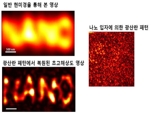 Ultra-high Resolution 2-dimentional Real-time Image Capture with Super Lens
Applications to high-precision semiconductor processing or intracellular structures observation are possible.
A joint research team led by Professors Yongkeun Park and Yong-Hoon Cho from the Department of Physics, KAIST, has succeeded in capturing real-time 2D images at a resolution of 100 nm (nanometers), which was impossible with optical lens due to the diffraction limit of light until now. Its future application includes high-precision semiconductor manufacturing process or observation of intracellular structures.
This research follows the past research of the super-lens developed by Professor Park last April, using paint spray to observe images that have three times higher resolution than those discovered by conventional optical lens.
Since optical lens utilize the refraction of light, the diffraction limit, which prevents achieving focus smaller than the wavelength of light, has always been a barrier for acquiring high-resolution images. In the past, it was impossible to observe objects less than the size of 200 to 300 nm in the visible light spectrum.
In order to solve the problem of near-field extinction due to scattering of light, the research team used spray paint consisting of nano-particles massed with dense scattering materials to obtain high-resolution information.
Then, by calculating and restoring the first scattering shape of light using the time reversibility of light, the researchers were able to overcome the diffraction limit. The original position of an object to be observed is obtained by deriving the complex trajectory of the light, and reversing the time to locate the particular position of the object.
Professor Park said, “This new technology can be used as the core technology in all fields which require optical measurement and control. The existing electron microscopy cannot observe cells without destroying them, but the new technology allows us to visualize at ultra-high resolution without destruction.”
The research results were published online in the 9th edition of Physical Review Letters, a prestigious international journal in the field of physics.
2014.09.23 View 10598
Ultra-high Resolution 2-dimentional Real-time Image Capture with Super Lens
Ultra-high Resolution 2-dimentional Real-time Image Capture with Super Lens
Applications to high-precision semiconductor processing or intracellular structures observation are possible.
A joint research team led by Professors Yongkeun Park and Yong-Hoon Cho from the Department of Physics, KAIST, has succeeded in capturing real-time 2D images at a resolution of 100 nm (nanometers), which was impossible with optical lens due to the diffraction limit of light until now. Its future application includes high-precision semiconductor manufacturing process or observation of intracellular structures.
This research follows the past research of the super-lens developed by Professor Park last April, using paint spray to observe images that have three times higher resolution than those discovered by conventional optical lens.
Since optical lens utilize the refraction of light, the diffraction limit, which prevents achieving focus smaller than the wavelength of light, has always been a barrier for acquiring high-resolution images. In the past, it was impossible to observe objects less than the size of 200 to 300 nm in the visible light spectrum.
In order to solve the problem of near-field extinction due to scattering of light, the research team used spray paint consisting of nano-particles massed with dense scattering materials to obtain high-resolution information.
Then, by calculating and restoring the first scattering shape of light using the time reversibility of light, the researchers were able to overcome the diffraction limit. The original position of an object to be observed is obtained by deriving the complex trajectory of the light, and reversing the time to locate the particular position of the object.
Professor Park said, “This new technology can be used as the core technology in all fields which require optical measurement and control. The existing electron microscopy cannot observe cells without destroying them, but the new technology allows us to visualize at ultra-high resolution without destruction.”
The research results were published online in the 9th edition of Physical Review Letters, a prestigious international journal in the field of physics.
2014.09.23 View 10598 -
 PIBOT, a small humanoid robot flies an aircraft
The 2014 IEEE/RSJ International Conference on Intelligent Robots and Systems (IROS 2014) took place in Chicago, Illinois, on September 14-18, 2014.
Professor David Hyunchul Shim and his students from the Department of Aerospace Engineering, KAIST, presented a research paper entitled “A Robot-machine Interface for Full-functionality Automation Using a Humanoid” at the conference.
The robot called “PIBOT,” a pint-sized, tiny humanoid robot, uses a mixture of flight data and visuals to fly an airplane, capable of identifying and operating all of the buttons and switches in the cockpit of a normal light aircraft designed for humans.
For now, the robot is only flying a simulator, but Professor Shim expects that “PIBOT will help us have a fully automated flight experience, eventually replacing human pilots.”
The IEEE Spectrum magazine published an article on PIBOT posted online September 18, 2014. Please follow the link below for the article:
IEEE Spectrum, September 18, 2014
Tiny Humanoid Robot Learning to Fly Real Airplanes
http://spectrum.ieee.org/automaton/robotics/humanoids/tiny-humanoid-robot-learning-to-fly-real-airplanes
2014.09.23 View 14330
PIBOT, a small humanoid robot flies an aircraft
The 2014 IEEE/RSJ International Conference on Intelligent Robots and Systems (IROS 2014) took place in Chicago, Illinois, on September 14-18, 2014.
Professor David Hyunchul Shim and his students from the Department of Aerospace Engineering, KAIST, presented a research paper entitled “A Robot-machine Interface for Full-functionality Automation Using a Humanoid” at the conference.
The robot called “PIBOT,” a pint-sized, tiny humanoid robot, uses a mixture of flight data and visuals to fly an airplane, capable of identifying and operating all of the buttons and switches in the cockpit of a normal light aircraft designed for humans.
For now, the robot is only flying a simulator, but Professor Shim expects that “PIBOT will help us have a fully automated flight experience, eventually replacing human pilots.”
The IEEE Spectrum magazine published an article on PIBOT posted online September 18, 2014. Please follow the link below for the article:
IEEE Spectrum, September 18, 2014
Tiny Humanoid Robot Learning to Fly Real Airplanes
http://spectrum.ieee.org/automaton/robotics/humanoids/tiny-humanoid-robot-learning-to-fly-real-airplanes
2014.09.23 View 14330 -
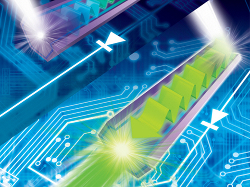 Development of a Photonic Diode with Light Speed, Single-Direction Transfer
A photonic diode using a nitride semiconductor rod can increase the possibility of developing all-optical integrated circuits, an alternative to conventional integrated circuits.
Professor Yong-Hoon Cho's research team from the Department of Physics, KAIST, developed a photonic diode which can selectively transfer light in one way, using semiconductor rods.
The photonic diode has a diameter of hundreds of nanometers (nm) and a length of few micrometers. This size enables its use in large-scale integration (LSI). The diode’s less sensitivity towards polarized light angle makes it more useful.
In an integrated circuit, a diode controls the flow of electrons. If this diode controls light rather than electrons, data can be transferred at high speed, and its loss is minimized to a greater extent. Since these implementations conserve more energy, this is a very promising future technology.
However, conventional electronic diodes, made up of asymmetric meta-materials or photonic crystalline structures, are large, which makes them difficult to be used in LSI. These diodes could only be implemented under limited conditions due to its sensitivity towards polarized light angle.
The research team used nitride semiconductor rods to develop a highly efficient photonic diode with distinct light intensities from opposite ends.
The semiconductor rod yields different amount of energy horizontally. According to the research team, this is because the width of the quantum well and its indium quantity is continuously controlled.
Professor Cho said, "A large energy difference in a horizontal direction causes asymmetrical light propagation, enabling it to be operated as a photonic diode." He added that “If light, instead of electrons, were adopted in integrated circuits, the transfer speed would be expected as great as that of light.”
The research findings were published in the September 10th issue of Nano Letters as the cover paper.
Under the guidance of Professor Cho, two Ph.D. candidates, Suk-Min Ko and Su-Hyun Gong, conducted this research. This research project was sponsored by the National Research Foundation of Korea and KAIST’s EEWS (energy, environment, water, and sustainability) Research Center.
Figure Description: Computer simulated image of photonic diode made of semiconductor rod implemented in an all-optical integrated circuit
2014.09.23 View 11984
Development of a Photonic Diode with Light Speed, Single-Direction Transfer
A photonic diode using a nitride semiconductor rod can increase the possibility of developing all-optical integrated circuits, an alternative to conventional integrated circuits.
Professor Yong-Hoon Cho's research team from the Department of Physics, KAIST, developed a photonic diode which can selectively transfer light in one way, using semiconductor rods.
The photonic diode has a diameter of hundreds of nanometers (nm) and a length of few micrometers. This size enables its use in large-scale integration (LSI). The diode’s less sensitivity towards polarized light angle makes it more useful.
In an integrated circuit, a diode controls the flow of electrons. If this diode controls light rather than electrons, data can be transferred at high speed, and its loss is minimized to a greater extent. Since these implementations conserve more energy, this is a very promising future technology.
However, conventional electronic diodes, made up of asymmetric meta-materials or photonic crystalline structures, are large, which makes them difficult to be used in LSI. These diodes could only be implemented under limited conditions due to its sensitivity towards polarized light angle.
The research team used nitride semiconductor rods to develop a highly efficient photonic diode with distinct light intensities from opposite ends.
The semiconductor rod yields different amount of energy horizontally. According to the research team, this is because the width of the quantum well and its indium quantity is continuously controlled.
Professor Cho said, "A large energy difference in a horizontal direction causes asymmetrical light propagation, enabling it to be operated as a photonic diode." He added that “If light, instead of electrons, were adopted in integrated circuits, the transfer speed would be expected as great as that of light.”
The research findings were published in the September 10th issue of Nano Letters as the cover paper.
Under the guidance of Professor Cho, two Ph.D. candidates, Suk-Min Ko and Su-Hyun Gong, conducted this research. This research project was sponsored by the National Research Foundation of Korea and KAIST’s EEWS (energy, environment, water, and sustainability) Research Center.
Figure Description: Computer simulated image of photonic diode made of semiconductor rod implemented in an all-optical integrated circuit
2014.09.23 View 11984 -
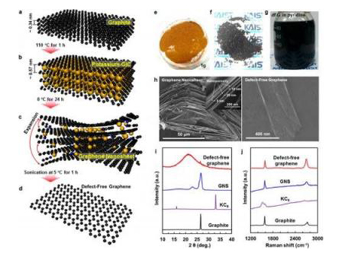 KAIST Researchers Fabricate Defect-free Graphene for Lithium-ion Batteries
Although graphene has been hailed as promising materials for lithium-ion batteries, making it for large-scale production has remained a challenging task for researchers. So far, high-quality graphene has been produced at the expense of large volume. It is possible to fabricate bulk quantities of graphene, but they will likely contain many defects.
Recently, a KAIST research team, headed by Professors Jung-Ki Park and Hee-Tak Kim from the Department of Chemical and Biomolecular Engineering, developed a fabrication method to produce a large amount of defect-free graphene (df-G) while preserving the structural integrity of the graphene.
This research result was published online in the July 11, 2014 issue of Nano Letters, entitled "Defect-free, Size-tunable Graphene for High-performance Lithium Ion Battery."
Phys.org, a science, research and technology news website, published an article on this research. To read article, please visit the link below:
Phys.org, August 22, 2014
“Scientists fabricate defect-free graphene, set record reversible capacity for Co3O4 node in Li-ion batteries”
http://phys.org/news/2014-08-scientists-fabricate-defect-free-graphene-reversible.html
2014.09.07 View 10391
KAIST Researchers Fabricate Defect-free Graphene for Lithium-ion Batteries
Although graphene has been hailed as promising materials for lithium-ion batteries, making it for large-scale production has remained a challenging task for researchers. So far, high-quality graphene has been produced at the expense of large volume. It is possible to fabricate bulk quantities of graphene, but they will likely contain many defects.
Recently, a KAIST research team, headed by Professors Jung-Ki Park and Hee-Tak Kim from the Department of Chemical and Biomolecular Engineering, developed a fabrication method to produce a large amount of defect-free graphene (df-G) while preserving the structural integrity of the graphene.
This research result was published online in the July 11, 2014 issue of Nano Letters, entitled "Defect-free, Size-tunable Graphene for High-performance Lithium Ion Battery."
Phys.org, a science, research and technology news website, published an article on this research. To read article, please visit the link below:
Phys.org, August 22, 2014
“Scientists fabricate defect-free graphene, set record reversible capacity for Co3O4 node in Li-ion batteries”
http://phys.org/news/2014-08-scientists-fabricate-defect-free-graphene-reversible.html
2014.09.07 View 10391