Nano
-
 Blood-Based Multiplexed Diagnostic Sensor Helps to Accurately Detect Alzheimer’s Disease
A research team at KAIST reported clinically accurate multiplexed electrical biosensor for detecting Alzheimer’s disease by measuring its core biomarkers using densely aligned carbon nanotubes.
Alzheimer’s disease is the most prevalent neurodegenerative disorder, affecting one in ten aged over 65 years. Early diagnosis can reduce the risk of suffering the disease by one-third, according to recent reports. However, its early diagnosis remains challenging due to the low accuracy but high cost of diagnosis.
Research team led by Professors Chan Beum Park and Steve Park described an ultrasensitive detection of multiple Alzheimer's disease core biomarker in human plasma. The team have designed the sensor array by employing a densely aligned single-walled carbon nanotube thin films as a transducer.
The representative biomarkers of Alzheimer's disease are beta-amyloid42, beta-amyloid40, total tau protein, phosphorylated tau protein and the concentrations of these biomarkers in human plasma are directly correlated with the pathology of Alzheimer’s disease.
The research team developed a highly sensitive resistive biosensor based on densely aligned carbon nanotubes fabricated by Langmuir-Blodgett method with a low manufacturing cost.
Aligned carbon nanotubes with high density minimizes the tube-to-tube junction resistance compared with randomly distributed carbon nanotubes, which leads to the improvement of sensor sensitivity. To be more specific, this resistive sensor with densely aligned carbon nanotubes exhibits a sensitivity over 100 times higher than that of conventional carbon nanotube-based biosensors.
By measuring the concentrations of four Alzheimer’s disease biomarkers simultaneously Alzheimer patients can be discriminated from health controls with an average sensitivity of 90.0%, a selectivity of 90.0% and an average accuracy of 88.6%.
This work, titled “Clinically accurate diagnosis of Alzheimer’s disease via multiplexed sensing of core biomarkers in human plasma”, were published in Nature Communications on January 8th 2020. The authors include PhD candidate Kayoung Kim and MS candidate Min-Ji Kim.
Professor Steve Park said, “This study was conducted on patients who are already confirmed with Alzheimer’s Disease. For further use in practical setting, it is necessary to test the patients with mild cognitive impairment.” He also emphasized that, “It is essential to establish a nationwide infrastructure, such as mild cognitive impairment cohort study and a dementia cohort study. This would enable the establishment of world-wide research network, and will help various private and public institutions.”
This research was supported by the Ministry of Science and ICT, Human Resource Bank of Chungnam National University Hospital and Chungbuk National University Hospital.
< A schematic diagram of a high-density aligned carbon nanotube-based resistive sensor that distinguishes patients with Alzheimer’s Disease by measuring the concentration of four biomarkers in the blood. >
Profile:
Professor Steve Park
stevepark@kaist.ac.kr
Department of Materials Science and Engineering
http://steveparklab.kaist.ac.kr/
KAIST
Profile:
Professor Chan Beum Park
parkcb at kaist.ac.kr
Department of Materials Science and Engineering
http://biomaterials.kaist.ac.kr/
KAIST
2020.02.07 View 12274
Blood-Based Multiplexed Diagnostic Sensor Helps to Accurately Detect Alzheimer’s Disease
A research team at KAIST reported clinically accurate multiplexed electrical biosensor for detecting Alzheimer’s disease by measuring its core biomarkers using densely aligned carbon nanotubes.
Alzheimer’s disease is the most prevalent neurodegenerative disorder, affecting one in ten aged over 65 years. Early diagnosis can reduce the risk of suffering the disease by one-third, according to recent reports. However, its early diagnosis remains challenging due to the low accuracy but high cost of diagnosis.
Research team led by Professors Chan Beum Park and Steve Park described an ultrasensitive detection of multiple Alzheimer's disease core biomarker in human plasma. The team have designed the sensor array by employing a densely aligned single-walled carbon nanotube thin films as a transducer.
The representative biomarkers of Alzheimer's disease are beta-amyloid42, beta-amyloid40, total tau protein, phosphorylated tau protein and the concentrations of these biomarkers in human plasma are directly correlated with the pathology of Alzheimer’s disease.
The research team developed a highly sensitive resistive biosensor based on densely aligned carbon nanotubes fabricated by Langmuir-Blodgett method with a low manufacturing cost.
Aligned carbon nanotubes with high density minimizes the tube-to-tube junction resistance compared with randomly distributed carbon nanotubes, which leads to the improvement of sensor sensitivity. To be more specific, this resistive sensor with densely aligned carbon nanotubes exhibits a sensitivity over 100 times higher than that of conventional carbon nanotube-based biosensors.
By measuring the concentrations of four Alzheimer’s disease biomarkers simultaneously Alzheimer patients can be discriminated from health controls with an average sensitivity of 90.0%, a selectivity of 90.0% and an average accuracy of 88.6%.
This work, titled “Clinically accurate diagnosis of Alzheimer’s disease via multiplexed sensing of core biomarkers in human plasma”, were published in Nature Communications on January 8th 2020. The authors include PhD candidate Kayoung Kim and MS candidate Min-Ji Kim.
Professor Steve Park said, “This study was conducted on patients who are already confirmed with Alzheimer’s Disease. For further use in practical setting, it is necessary to test the patients with mild cognitive impairment.” He also emphasized that, “It is essential to establish a nationwide infrastructure, such as mild cognitive impairment cohort study and a dementia cohort study. This would enable the establishment of world-wide research network, and will help various private and public institutions.”
This research was supported by the Ministry of Science and ICT, Human Resource Bank of Chungnam National University Hospital and Chungbuk National University Hospital.
< A schematic diagram of a high-density aligned carbon nanotube-based resistive sensor that distinguishes patients with Alzheimer’s Disease by measuring the concentration of four biomarkers in the blood. >
Profile:
Professor Steve Park
stevepark@kaist.ac.kr
Department of Materials Science and Engineering
http://steveparklab.kaist.ac.kr/
KAIST
Profile:
Professor Chan Beum Park
parkcb at kaist.ac.kr
Department of Materials Science and Engineering
http://biomaterials.kaist.ac.kr/
KAIST
2020.02.07 View 12274 -
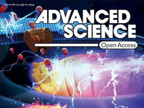 Researchers Describe a Mechanism Inducing Self-Killing of Cancer Cells
(Professor Kim (left) and lead author Lee)
Researchers have described a new mechanism which induces the self-killing of cancer cells by perturbing ion homeostasis. A research team from the Department of Biochemical Engineering has developed helical polypeptide potassium ionophores that lead to the onset of programmed cell death. The ionophores increase the active oxygen concentration to stress endoplasmic reticulum to the point of cellular death.
The electrochemical gradient between extracellular and intracellular conditions plays an important role in cell growth and metabolism. When a cell’s ion homeostasis is disturbed, critical functions accelerating the activation of apoptosis are inhibited in the cell.
Although ionophores have been intensively used as an ion homeostasis disturber, the mechanisms of cell death have been unclear and the bio-applicability has been limited. In the study featured at Advanced Science, the team presented an alpha helical peptide-based anticancer agent that is capable of transporting potassium ions with water solubility. The cationic, hydrophilic, and potassium ionic groups were combined at the end of the peptide side chain to provide both ion transport and hydrophilic properties.
These peptide-based ionophores reduce the intracellular potassium concentration and at the same time increase the intracellular calcium concentration. Increased intracellular calcium concentrations produce intracellular reactive oxygen species, causing endoplasmic reticulum stress, and ultimately leading to apoptosis.
Anticancer effects were evaluated using tumor-bearing mice to confirm the therapeutic effect, even in animal models. It was found that tumor growth was strongly inhibited by endoplasmic stress-mediated apoptosis.
Lead author Dr. Dae-Yong Lee said, “A peptide-based ionophore is more effective than conventional chemotherapeutic agents because it induces apoptosis via elevated reactive oxygen species levels. Professor Yeu-Chun Kim said he expects this new mechanism to be widely used as a new chemotherapeutic strategy. This research was funded by the National Research Foundation.
2019.08.28 View 21867
Researchers Describe a Mechanism Inducing Self-Killing of Cancer Cells
(Professor Kim (left) and lead author Lee)
Researchers have described a new mechanism which induces the self-killing of cancer cells by perturbing ion homeostasis. A research team from the Department of Biochemical Engineering has developed helical polypeptide potassium ionophores that lead to the onset of programmed cell death. The ionophores increase the active oxygen concentration to stress endoplasmic reticulum to the point of cellular death.
The electrochemical gradient between extracellular and intracellular conditions plays an important role in cell growth and metabolism. When a cell’s ion homeostasis is disturbed, critical functions accelerating the activation of apoptosis are inhibited in the cell.
Although ionophores have been intensively used as an ion homeostasis disturber, the mechanisms of cell death have been unclear and the bio-applicability has been limited. In the study featured at Advanced Science, the team presented an alpha helical peptide-based anticancer agent that is capable of transporting potassium ions with water solubility. The cationic, hydrophilic, and potassium ionic groups were combined at the end of the peptide side chain to provide both ion transport and hydrophilic properties.
These peptide-based ionophores reduce the intracellular potassium concentration and at the same time increase the intracellular calcium concentration. Increased intracellular calcium concentrations produce intracellular reactive oxygen species, causing endoplasmic reticulum stress, and ultimately leading to apoptosis.
Anticancer effects were evaluated using tumor-bearing mice to confirm the therapeutic effect, even in animal models. It was found that tumor growth was strongly inhibited by endoplasmic stress-mediated apoptosis.
Lead author Dr. Dae-Yong Lee said, “A peptide-based ionophore is more effective than conventional chemotherapeutic agents because it induces apoptosis via elevated reactive oxygen species levels. Professor Yeu-Chun Kim said he expects this new mechanism to be widely used as a new chemotherapeutic strategy. This research was funded by the National Research Foundation.
2019.08.28 View 21867 -
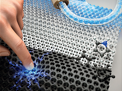 Highly Uniform and Low Hysteresis Pressure Sensor to Increase Practical Applicability
< Professor Steve Park (left) and the First Author Mr. Jinwon Oh (right) >
Researchers have designed a flexible pressure sensor that is expected to have a much wider applicability. A KAIST research team fabricated a piezoresistive pressure sensor of high uniformity with low hysteresis by chemically grafting a conductive polymer onto a porous elastomer template.
The team discovered that the uniformity of pore size and shape is directly related to the uniformity of the sensor. The team noted that by increasing pore size and shape variability, the variability of the sensor characteristics also increases.
Researchers led by Professor Steve Park from the Department of Materials Science and Engineering confirmed that compared to other sensors composed of randomly sized and shaped pores, which had a coefficient of variation in relative resistance change of 69.65%, their newly developed sensor exhibited much higher uniformity with a coefficient of variation of 2.43%. This study was reported in Small as the cover article on August 16.
Flexible pressure sensors have been actively researched and widely applied in electronic equipment such as touch screens, robots, wearable healthcare devices, electronic skin, and human-machine interfaces. In particular, piezoresistive pressure sensors based on elastomer‐conductive material composites hold significant potential due to their many advantages including a simple and low-cost fabrication process.
Various research results have been reported for ways to improve the performance of piezoresistive pressure sensors, most of which have been focused on increasing the sensitivity. Despite its significance, maximizing the sensitivity of composite-based piezoresistive pressure sensors is not necessary for many applications. On the other hand, sensor-to-sensor uniformity and hysteresis are two properties that are of critical importance to realize any application.
The importance of sensor-to-sensor uniformity is obvious. If the sensors manufactured under the same conditions have different properties, measurement reliability is compromised, and therefore the sensor cannot be used in a practical setting.
In addition, low hysteresis is also essential for improved measurement reliability. Hysteresis is a phenomenon in which the electrical readings differ depending on how fast or slow the sensor is being pressed, whether pressure is being released or applied, and how long and to what degree the sensor has been pressed. When a sensor has high hysteresis, the electrical readings will differ even under the same pressure, making the measurements unreliable.
Researchers said they observed a negligible hysteresis degree which was only 2%. This was attributed to the strong chemical bonding between the conductive polymer and the elastomer template, which prevents their relative sliding and displacement, and the porosity of the elastomer that enhances elastic behavior.
“This technology brings forth insight into how to address the two critical issues in pressure sensors: uniformity and hysteresis. We expect our technology to play an important role in increasing practical applications and the commercialization of pressure sensors in the near future,” said Professor Park.
This work was conducted as part of the KAIST‐funded Global Singularity Research Program for 2019, and also supported by the KUSTAR‐KAIST Institute.
Figure 1. Image of a porous elastomer template with uniform pore size and shape (left), Graph showing high uniformity in the sensors’ performance (right).
Figure 2. Hysteresis loops of the sensor at different pressure levels (left), and after a different number of cycles (right).
Figure 3. The cover page of Small Journal, Volume 15, Issue 33.
Publication:
Jinwon Oh, Jin‐Oh Kim, Yunjoo Kim, Han Byul Choi, Jun Chang Yang, Serin Lee, Mikhail Pyatykh, Jung Kim, Joo Yong Sim, and Steve Park. 2019. Highly Uniform and Low Hysteresis Piezoresistive Pressure Sensors Based on Chemical Grafting of Polypyrrole on Elastomer Template with Uniform Pore Size. Small. Wiley-VCH Verlag GmbH & Co. KgaA, Weinheim, Germany, Volume No. 15, Issue No. 33, Full Paper No. 201901744, 8 pages. https://doi.org/10.1002/smll.201901744
Profile: Prof. Steve Park, MS, PhD
stevepark@kaist.ac.kr
http://steveparklab.kaist.ac.kr/
Assistant Professor
Organic and Nano Electronics Laboratory
Department of Materials Science and Engineering
Korea Advanced Institute of Science and Technology (KAIST)
http://kaist.ac.kr
Daejeon 34141, Korea
Profile: Mr. Jinwon Oh, MS
jwoh1701@gmail.com
http://steveparklab.kaist.ac.kr/
Researcher
Organic and Nano Electronics Laboratory
Department of Materials Science and Engineering
Korea Advanced Institute of Science and Technology (KAIST)
http://kaist.ac.kr Daejeon 34141, Korea
Profile: Prof. Jung Kim, MS, PhD
jungkim@kaist.ac.kr
http://medev.kaist.ac.kr/
Professor
Biorobotics Laboratory
Department of Mechanical Engineering
Korea Advanced Institute of Science and Technology (KAIST)
http://kaist.ac.kr Daejeon 34141, Korea
Profile: Joo Yong Sim, PhD
jsim@etri.re.kr
Researcher
Bio-Medical IT Convergence Research Department
Electronics and Telecommunications Research Institute (ETRI)
https://www.etri.re.krDaejeon 34129, Korea
(END)
2019.08.19 View 29443
Highly Uniform and Low Hysteresis Pressure Sensor to Increase Practical Applicability
< Professor Steve Park (left) and the First Author Mr. Jinwon Oh (right) >
Researchers have designed a flexible pressure sensor that is expected to have a much wider applicability. A KAIST research team fabricated a piezoresistive pressure sensor of high uniformity with low hysteresis by chemically grafting a conductive polymer onto a porous elastomer template.
The team discovered that the uniformity of pore size and shape is directly related to the uniformity of the sensor. The team noted that by increasing pore size and shape variability, the variability of the sensor characteristics also increases.
Researchers led by Professor Steve Park from the Department of Materials Science and Engineering confirmed that compared to other sensors composed of randomly sized and shaped pores, which had a coefficient of variation in relative resistance change of 69.65%, their newly developed sensor exhibited much higher uniformity with a coefficient of variation of 2.43%. This study was reported in Small as the cover article on August 16.
Flexible pressure sensors have been actively researched and widely applied in electronic equipment such as touch screens, robots, wearable healthcare devices, electronic skin, and human-machine interfaces. In particular, piezoresistive pressure sensors based on elastomer‐conductive material composites hold significant potential due to their many advantages including a simple and low-cost fabrication process.
Various research results have been reported for ways to improve the performance of piezoresistive pressure sensors, most of which have been focused on increasing the sensitivity. Despite its significance, maximizing the sensitivity of composite-based piezoresistive pressure sensors is not necessary for many applications. On the other hand, sensor-to-sensor uniformity and hysteresis are two properties that are of critical importance to realize any application.
The importance of sensor-to-sensor uniformity is obvious. If the sensors manufactured under the same conditions have different properties, measurement reliability is compromised, and therefore the sensor cannot be used in a practical setting.
In addition, low hysteresis is also essential for improved measurement reliability. Hysteresis is a phenomenon in which the electrical readings differ depending on how fast or slow the sensor is being pressed, whether pressure is being released or applied, and how long and to what degree the sensor has been pressed. When a sensor has high hysteresis, the electrical readings will differ even under the same pressure, making the measurements unreliable.
Researchers said they observed a negligible hysteresis degree which was only 2%. This was attributed to the strong chemical bonding between the conductive polymer and the elastomer template, which prevents their relative sliding and displacement, and the porosity of the elastomer that enhances elastic behavior.
“This technology brings forth insight into how to address the two critical issues in pressure sensors: uniformity and hysteresis. We expect our technology to play an important role in increasing practical applications and the commercialization of pressure sensors in the near future,” said Professor Park.
This work was conducted as part of the KAIST‐funded Global Singularity Research Program for 2019, and also supported by the KUSTAR‐KAIST Institute.
Figure 1. Image of a porous elastomer template with uniform pore size and shape (left), Graph showing high uniformity in the sensors’ performance (right).
Figure 2. Hysteresis loops of the sensor at different pressure levels (left), and after a different number of cycles (right).
Figure 3. The cover page of Small Journal, Volume 15, Issue 33.
Publication:
Jinwon Oh, Jin‐Oh Kim, Yunjoo Kim, Han Byul Choi, Jun Chang Yang, Serin Lee, Mikhail Pyatykh, Jung Kim, Joo Yong Sim, and Steve Park. 2019. Highly Uniform and Low Hysteresis Piezoresistive Pressure Sensors Based on Chemical Grafting of Polypyrrole on Elastomer Template with Uniform Pore Size. Small. Wiley-VCH Verlag GmbH & Co. KgaA, Weinheim, Germany, Volume No. 15, Issue No. 33, Full Paper No. 201901744, 8 pages. https://doi.org/10.1002/smll.201901744
Profile: Prof. Steve Park, MS, PhD
stevepark@kaist.ac.kr
http://steveparklab.kaist.ac.kr/
Assistant Professor
Organic and Nano Electronics Laboratory
Department of Materials Science and Engineering
Korea Advanced Institute of Science and Technology (KAIST)
http://kaist.ac.kr
Daejeon 34141, Korea
Profile: Mr. Jinwon Oh, MS
jwoh1701@gmail.com
http://steveparklab.kaist.ac.kr/
Researcher
Organic and Nano Electronics Laboratory
Department of Materials Science and Engineering
Korea Advanced Institute of Science and Technology (KAIST)
http://kaist.ac.kr Daejeon 34141, Korea
Profile: Prof. Jung Kim, MS, PhD
jungkim@kaist.ac.kr
http://medev.kaist.ac.kr/
Professor
Biorobotics Laboratory
Department of Mechanical Engineering
Korea Advanced Institute of Science and Technology (KAIST)
http://kaist.ac.kr Daejeon 34141, Korea
Profile: Joo Yong Sim, PhD
jsim@etri.re.kr
Researcher
Bio-Medical IT Convergence Research Department
Electronics and Telecommunications Research Institute (ETRI)
https://www.etri.re.krDaejeon 34129, Korea
(END)
2019.08.19 View 29443 -
 Enhanced Natural Gas Storage to Help Reduce Global Warming
< Professor Atilhan (left) and Professor Yavuz (right) >
Researchers have designed plastic-based materials that can store natural gas more effectively. These new materials can not only make large-scale, cost-effective, and safe natural gas storage possible, but further hold a strong promise for combating global warming.
Natural gas (predominantly methane) is a clean energy alternative. It is stored by compression, liquefaction, or adsorption. Among these, adsorbed natural gas (ANG) storage is a more efficient, cheaper, and safer alternative to conventional compressed natural gas (CNG) and liquefied natural gas (LNG) storage approaches that have drawbacks such as low storage efficiency, high costs, and safety concerns. However, developing adsorptive materials that can more fully exploit the advantages of ANG storage has remained a challenging task.
A KAIST research team led by Professor Cafer T. Yavuz from the Graduate School of Energy, Environment, Water, and Sustainability (EEWS), in collaboration with Professor Mert Atilhan’s group from Texas A&M University, synthesized 29 unique porous polymeric structures with inherent flexibility, and tested their methane gas uptake capacity at high pressures. These porous polymers had varying synthetic complexities, porosities, and morphologies, and the researchers subjected each porous polymer to pure methane gas under various conditions to study the ANG performances.
Of these 29 distinct chemical structures, COP-150 was particularly noteworthy as it achieved a high deliverable gravimetric methane working capacity when cycled between 5 and 100 bar at 273 K, which is 98% of the total uptake capacity. This result surpassed the target set by the United States Department of Energy (US DOE).
COP-150 is the first ever structure to fulfil both the gravimetric and volumetric requirements of the US DOE for successful vehicular use, and the total cost to produce the COP-150 adsorbent was only 1 USD per kilogram.
COP-150 can be produced using freely available and easily accessible plastic materials, and moreover, its synthesis takes place at room temperature, open to the air, and no previous purification of the chemicals is required. The pressure-triggered flexible structure of COP-150 is also advantageous in terms of the total working capacity of deliverable methane for real applications.
The research team believed that the increased pressure flexes the network structure of COP-150 showing “swelling” behavior, and suggested that the flexibility provides rapid desorption and thermal management, while the hydrophobicity and the nature of the covalently bonded framework allow these promising materials to tolerate harsh conditions.
This swelling mechanism of expansion-contraction solves two other major issues, the team noted. Firstly, when using adsorbents based on such a mechanism, unsafe pressure spikes that may occur due to temperature swings can be eliminated. In addition, contamination can also be minimized, since the adsorbent remains contracted when no gas is stored.
Professor Yavuz said, “We envision a whole host of new designs and mechanisms to be developed based on our concept. Since natural gas is a much cleaner fuel than coal and petroleum, new developments in this realm will help switching to the use of less polluting fuels.”
Professor Atilhan agreed the most important impact of their research is on the environment. “Using natural gas more than coal and petroleum will significantly reduce greenhouse gas emissions. We believe, one day, we might see vehicles equipped with our materials that are run by a cleaner natural gas fuel,” he added.
This study, reported in Nature Energy on July 8, was supported by National Research Foundation of Korea (NRF) grants ( NRF-2016R1A2B4011027, NRF-2017M3A7B4042140, and NRF-2017M3A7B4042235).
< Suggested chemical structure of COP-150 >
< Initial ingredients (left) and final product (right) of COP-150 synthesis >
< Comparison of highest reported volumetric working capacities >
(END)
2019.08.09 View 28179
Enhanced Natural Gas Storage to Help Reduce Global Warming
< Professor Atilhan (left) and Professor Yavuz (right) >
Researchers have designed plastic-based materials that can store natural gas more effectively. These new materials can not only make large-scale, cost-effective, and safe natural gas storage possible, but further hold a strong promise for combating global warming.
Natural gas (predominantly methane) is a clean energy alternative. It is stored by compression, liquefaction, or adsorption. Among these, adsorbed natural gas (ANG) storage is a more efficient, cheaper, and safer alternative to conventional compressed natural gas (CNG) and liquefied natural gas (LNG) storage approaches that have drawbacks such as low storage efficiency, high costs, and safety concerns. However, developing adsorptive materials that can more fully exploit the advantages of ANG storage has remained a challenging task.
A KAIST research team led by Professor Cafer T. Yavuz from the Graduate School of Energy, Environment, Water, and Sustainability (EEWS), in collaboration with Professor Mert Atilhan’s group from Texas A&M University, synthesized 29 unique porous polymeric structures with inherent flexibility, and tested their methane gas uptake capacity at high pressures. These porous polymers had varying synthetic complexities, porosities, and morphologies, and the researchers subjected each porous polymer to pure methane gas under various conditions to study the ANG performances.
Of these 29 distinct chemical structures, COP-150 was particularly noteworthy as it achieved a high deliverable gravimetric methane working capacity when cycled between 5 and 100 bar at 273 K, which is 98% of the total uptake capacity. This result surpassed the target set by the United States Department of Energy (US DOE).
COP-150 is the first ever structure to fulfil both the gravimetric and volumetric requirements of the US DOE for successful vehicular use, and the total cost to produce the COP-150 adsorbent was only 1 USD per kilogram.
COP-150 can be produced using freely available and easily accessible plastic materials, and moreover, its synthesis takes place at room temperature, open to the air, and no previous purification of the chemicals is required. The pressure-triggered flexible structure of COP-150 is also advantageous in terms of the total working capacity of deliverable methane for real applications.
The research team believed that the increased pressure flexes the network structure of COP-150 showing “swelling” behavior, and suggested that the flexibility provides rapid desorption and thermal management, while the hydrophobicity and the nature of the covalently bonded framework allow these promising materials to tolerate harsh conditions.
This swelling mechanism of expansion-contraction solves two other major issues, the team noted. Firstly, when using adsorbents based on such a mechanism, unsafe pressure spikes that may occur due to temperature swings can be eliminated. In addition, contamination can also be minimized, since the adsorbent remains contracted when no gas is stored.
Professor Yavuz said, “We envision a whole host of new designs and mechanisms to be developed based on our concept. Since natural gas is a much cleaner fuel than coal and petroleum, new developments in this realm will help switching to the use of less polluting fuels.”
Professor Atilhan agreed the most important impact of their research is on the environment. “Using natural gas more than coal and petroleum will significantly reduce greenhouse gas emissions. We believe, one day, we might see vehicles equipped with our materials that are run by a cleaner natural gas fuel,” he added.
This study, reported in Nature Energy on July 8, was supported by National Research Foundation of Korea (NRF) grants ( NRF-2016R1A2B4011027, NRF-2017M3A7B4042140, and NRF-2017M3A7B4042235).
< Suggested chemical structure of COP-150 >
< Initial ingredients (left) and final product (right) of COP-150 synthesis >
< Comparison of highest reported volumetric working capacities >
(END)
2019.08.09 View 28179 -
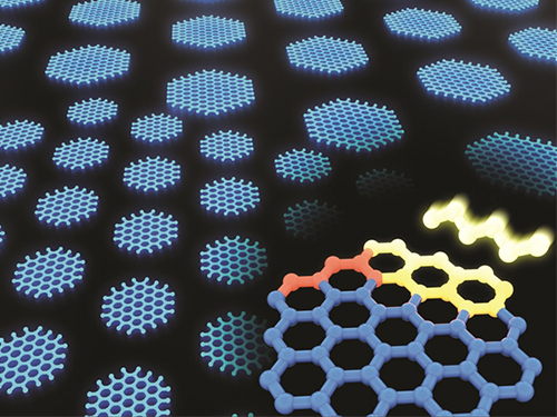 Synthesizing Single-Crystalline Hexagonal Graphene Quantum Dots
(Figure: Uniformly ordered single-crystalline graphene quantum dots of various sizes synthesized through solution chemistry.)
A KAIST team has designed a novel strategy for synthesizing single-crystalline graphene quantum dots, which emit stable blue light. The research team confirmed that a display made of their synthesized graphene quantum dots successfully emitted blue light with stable electric pressure, reportedly resolving the long-standing challenges of blue light emission in manufactured displays. The study, led by Professor O Ok Park in the Department of Chemical and Biological Engineering, was featured online in Nano Letters on July 5.
Graphene has gained increased attention as a next-generation material for its heat and electrical conductivity as well as its transparency. However, single and multi-layered graphene have characteristics of a conductor so that it is difficult to apply into semiconductor. Only when downsized to the nanoscale, semiconductor’s distinct feature of bandgap will be exhibited to emit the light in the graphene. This illuminating featuring of dot is referred to as a graphene quantum dot.
Conventionally, single-crystalline graphene has been fabricated by chemical vapor deposition (CVD) on copper or nickel thin films, or by peeling graphite physically and chemically. However, graphene made via chemical vapor deposition is mainly used for large-surface transparent electrodes. Meanwhile, graphene made by chemical and physical peeling carries uneven size defects.
The research team explained that their graphene quantum dots exhibited a very stable single-phase reaction when they mixed amine and acetic acid with an aqueous solution of glucose. Then, they synthesized single-crystalline graphene quantum dots from the self-assembly of the reaction intermediate. In the course of fabrication, the team developed a new separation method at a low-temperature precipitation, which led to successfully creating a homogeneous nucleation of graphene quantum dots via a single-phase reaction.
Professor Park and his colleagues have developed solution phase synthesis technology that allows for the creation of the desired crystal size for single nanocrystals down to 100 nano meters. It is reportedly the first synthesis of the homogeneous nucleation of graphene through a single-phase reaction.
Professor Park said, "This solution method will significantly contribute to the grafting of graphene in various fields. The application of this new graphene will expand the scope of its applications such as for flexible displays and varistors.”
This research was a joint project with a team from Korea University under Professor Sang Hyuk Im from the Department of Chemical and Biological Engineering, and was supported by the National Research Foundation of Korea, the Nano-Material Technology Development Program from the Electronics and Telecommunications Research Institute (ETRI), KAIST EEWS, and the BK21+ project from the Korean government.
2019.08.02 View 35344
Synthesizing Single-Crystalline Hexagonal Graphene Quantum Dots
(Figure: Uniformly ordered single-crystalline graphene quantum dots of various sizes synthesized through solution chemistry.)
A KAIST team has designed a novel strategy for synthesizing single-crystalline graphene quantum dots, which emit stable blue light. The research team confirmed that a display made of their synthesized graphene quantum dots successfully emitted blue light with stable electric pressure, reportedly resolving the long-standing challenges of blue light emission in manufactured displays. The study, led by Professor O Ok Park in the Department of Chemical and Biological Engineering, was featured online in Nano Letters on July 5.
Graphene has gained increased attention as a next-generation material for its heat and electrical conductivity as well as its transparency. However, single and multi-layered graphene have characteristics of a conductor so that it is difficult to apply into semiconductor. Only when downsized to the nanoscale, semiconductor’s distinct feature of bandgap will be exhibited to emit the light in the graphene. This illuminating featuring of dot is referred to as a graphene quantum dot.
Conventionally, single-crystalline graphene has been fabricated by chemical vapor deposition (CVD) on copper or nickel thin films, or by peeling graphite physically and chemically. However, graphene made via chemical vapor deposition is mainly used for large-surface transparent electrodes. Meanwhile, graphene made by chemical and physical peeling carries uneven size defects.
The research team explained that their graphene quantum dots exhibited a very stable single-phase reaction when they mixed amine and acetic acid with an aqueous solution of glucose. Then, they synthesized single-crystalline graphene quantum dots from the self-assembly of the reaction intermediate. In the course of fabrication, the team developed a new separation method at a low-temperature precipitation, which led to successfully creating a homogeneous nucleation of graphene quantum dots via a single-phase reaction.
Professor Park and his colleagues have developed solution phase synthesis technology that allows for the creation of the desired crystal size for single nanocrystals down to 100 nano meters. It is reportedly the first synthesis of the homogeneous nucleation of graphene through a single-phase reaction.
Professor Park said, "This solution method will significantly contribute to the grafting of graphene in various fields. The application of this new graphene will expand the scope of its applications such as for flexible displays and varistors.”
This research was a joint project with a team from Korea University under Professor Sang Hyuk Im from the Department of Chemical and Biological Engineering, and was supported by the National Research Foundation of Korea, the Nano-Material Technology Development Program from the Electronics and Telecommunications Research Institute (ETRI), KAIST EEWS, and the BK21+ project from the Korean government.
2019.08.02 View 35344 -
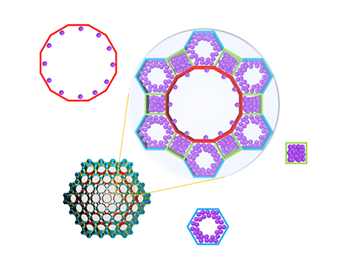 Real-Time Analysis of MOF Adsorption Behavior
Researchers have developed a technology to analyze the adsorption behavior of molecules in each individual pore of a metal organic framework (MOF). This system has large specific surface areas, allowing for the real-time observation of the adsorption process of an MOF, a new material effective for sorting carbon dioxide, hydrogen, and methane.
Accurate measurements and assessments of gas adsorption isotherms are important for characterizing porous materials and developing their applications. The existing technology is only able to measure the amount of gas molecules adsorbed to the material, without directly observing the adsorption behavior.
The research team led by Professor Jeung Ku Kang from the Graduate School of Energy, Environment, Water and Sustainability (EEWS) prescribed a real time gas adsorption crystallography system by integrating an existing X-ray diffraction (XRD) measurement device that can provide structural information and a gas adsorption measurement device.
Specifically, the system allowed the observation of a mesoporous MOF that has multiple pores rather than a single pore structure. The research team categorized the adsorption behaviors of MOF molecules by pore type, followed by observations and measurements, resulting in the identification of a stepwise adsorption process that was previously not possible to analyze.
Further, the team systematically and quantitatively analyzed how the pore structure and the type of adsorption molecule affect the adsorption behavior to suggest what type of MOF structure is appropriate as a storage material for each type of adsorption behavior.
Professor Kang said, “We quantitatively analyzed each pore molecule in real time to identify the effects of chemical and structural properties of pores on adsorption behavior.” He continued, “By understanding the real-time adsorption behavior of molecules at the level of the pores that form the material, rather than the whole material, we will be able to apply this technology to develop a new high-capacity storage material.”
This research was published in Nature Chemistry online on May 13, 2019 under the title ‘Isotherms of Individual Pores by Gas Adsorption Crystallography’.
(Figure. Schematic illustration of molecules adsorbed on metal organic frameworks with different pores of various structures, where the In-situ X-ray crystallography has been developed to classify each pore structure and analyze the position of the molecule to determine the amount of molecules adsorbed to each pore.)
2019.06.18 View 39948
Real-Time Analysis of MOF Adsorption Behavior
Researchers have developed a technology to analyze the adsorption behavior of molecules in each individual pore of a metal organic framework (MOF). This system has large specific surface areas, allowing for the real-time observation of the adsorption process of an MOF, a new material effective for sorting carbon dioxide, hydrogen, and methane.
Accurate measurements and assessments of gas adsorption isotherms are important for characterizing porous materials and developing their applications. The existing technology is only able to measure the amount of gas molecules adsorbed to the material, without directly observing the adsorption behavior.
The research team led by Professor Jeung Ku Kang from the Graduate School of Energy, Environment, Water and Sustainability (EEWS) prescribed a real time gas adsorption crystallography system by integrating an existing X-ray diffraction (XRD) measurement device that can provide structural information and a gas adsorption measurement device.
Specifically, the system allowed the observation of a mesoporous MOF that has multiple pores rather than a single pore structure. The research team categorized the adsorption behaviors of MOF molecules by pore type, followed by observations and measurements, resulting in the identification of a stepwise adsorption process that was previously not possible to analyze.
Further, the team systematically and quantitatively analyzed how the pore structure and the type of adsorption molecule affect the adsorption behavior to suggest what type of MOF structure is appropriate as a storage material for each type of adsorption behavior.
Professor Kang said, “We quantitatively analyzed each pore molecule in real time to identify the effects of chemical and structural properties of pores on adsorption behavior.” He continued, “By understanding the real-time adsorption behavior of molecules at the level of the pores that form the material, rather than the whole material, we will be able to apply this technology to develop a new high-capacity storage material.”
This research was published in Nature Chemistry online on May 13, 2019 under the title ‘Isotherms of Individual Pores by Gas Adsorption Crystallography’.
(Figure. Schematic illustration of molecules adsorbed on metal organic frameworks with different pores of various structures, where the In-situ X-ray crystallography has been developed to classify each pore structure and analyze the position of the molecule to determine the amount of molecules adsorbed to each pore.)
2019.06.18 View 39948 -
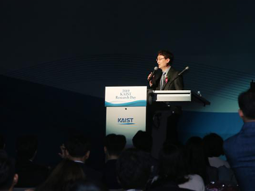 Research Day Highlights Most Outstanding Research Achievements
Professor Byung Jin Cho from the School of Electrical Engineering was selected as the Grand Research Prize Winner in recognition of his innovative research achievement in the fields of nano electric and flexible energy devices during the 2019 KAIST Research Day ceremony held on April 23 at the Chung Kunmo Conference Hall.
The ten most outstanding research achievements from the past year were also awarded in the three areas of Research, Innovation, Convergence Researches.
Professor Cho is an internationally recognized researcher in the field of future nano and energy device technology. Professor Cho’s team has continued to research on advanced CMOS (complementary metal-oxide semiconductors). CMOS has become his key research topic over the past three decades.
In 2014, he developed a glass fabric-based thermoelectric generator, which is extremely light and flexible and produces electricity from the heat of the human body. It is so flexible that the allowable bending radius of the generator is as low as 20 mm. There are no changes in performance even if the generator bends upward and downward for up to 120 cycles. His wearable thermoelectric generator was selected as one of the top ten most promising digital technologies by the Netexplo Forum in 2015.
He now is working on high-performance and ultra-flexible CMOS IC for biomedical applications, expanding his scope to thermal haptic technology in VR using graphene-CMOS hybrid integrated circuits; to self-powered wireless sensor nodes and self-powered ECG system using wearable thermoelectric generators .
In his special lecture at the ceremony, Professor Cho stressed the importance of collaboration in making scientific research and presented how he moved to future devices after focusing on scaling the devices.
“When I started the research on semiconductors, I focused on how to scale the device down as much as possible. For decades, we have conducted a number of procedures to produce tiny but efficient materials. Now we have shifted to develop flexible thermoelements and wearable devices,” said Professor Cho.
“We all thought the scaling down is the only way to create value-added technological breakthroughs. Now, the devices have been scaled down to 7nm and will go down to 5 nm soon. Over the past few years, I think we have gone through all the possible technological breakthroughs for reducing the size to 5nm. The semiconductor devices are made of more 1 billion transistors and go through 1,000 technological processes. So, there won’t be any possible way for a single genius to make a huge breakthrough. Without collaboration with others, it is nearly impossible to make any new technological breakthroughs.”
Professor Cho has published more than 240 papers in renowned academic journals and presented more than 300 papers at academic conferences. He has also registered approximately 50 patents in the field of semiconductor device technology.
The top ten research highlights of 2018 as follows:
- Rydberg-Atom Quantum Simulator Development by Professor Jaewook Ahn and Heung-Sun Sim from the Department of Physics
- From C-H to C-C Bonds at Room Temperature by Professor Mu-Hyun Baik from the Department of Chemistry
- The Role of Rodlike Counterions on the Interactions of DNAs by Professor Yong Woon Kim of the Graduate School of Nanoscience and Technology
- The Medal Preoptic Area Induces Hunting-Like Behaviors to Target Objects and Prey by Professor Daesoo Kim from the Department of Biological Sciences
- Identification of the Origin of Brain Tumors and New Therapeutic Strategy by Professor Jeong Ho Lee from the Graduate School of Medical Science and Engineering
- The Linear Frequency Conversion of Light at a Spatiotemporal Boundary by Professor Bumki Min from the Department of Mechanical Engineering
- An Industrial Grade Flexible Transparent Force Touch Sensor by Professor Jun-Bo Yoon from the School of Electrical Engineering
- The Detection and Clustering of Mixed-Type Defect Patterns in Wafer Bin Maps by Professor Heeyoung Kim from the Department of Industrial and Systems Engineering
- The Development of a Reconfigurable Spin-Based Logic Device by Professor Byong-Guk Park from the Department of Materials Science and Engineering
- The Development of a Miniaturized X-Ray Tube Based on Carbon Nanotube and Electronic Brachytherapy Device by Professor Sung Oh Cho from the Department of Nuclear and Quantum Engineering
Professor YongKeun Park from the Department of Physics and Professor In-Chel Park from the School of Electrical Engineering received the Research Award. For the Innovation Award, Professor Munchurl Kim from the School of Electrical Engineering was the recipient and the Convergence Research Awards was conferred to Professor Sung-Yool Choi from the School of Electrical Engineering, Professor Sung Gap Im from the Department of Chemical and Biomolecular Engineering, and Professor SangHee Park from the Department of Materials Science and Engineering during the ceremony.
For more on KAIST’s Top Research Achievements and Highlight of 2018, please refer to the attached below. click.
2019.04.25 View 17719
Research Day Highlights Most Outstanding Research Achievements
Professor Byung Jin Cho from the School of Electrical Engineering was selected as the Grand Research Prize Winner in recognition of his innovative research achievement in the fields of nano electric and flexible energy devices during the 2019 KAIST Research Day ceremony held on April 23 at the Chung Kunmo Conference Hall.
The ten most outstanding research achievements from the past year were also awarded in the three areas of Research, Innovation, Convergence Researches.
Professor Cho is an internationally recognized researcher in the field of future nano and energy device technology. Professor Cho’s team has continued to research on advanced CMOS (complementary metal-oxide semiconductors). CMOS has become his key research topic over the past three decades.
In 2014, he developed a glass fabric-based thermoelectric generator, which is extremely light and flexible and produces electricity from the heat of the human body. It is so flexible that the allowable bending radius of the generator is as low as 20 mm. There are no changes in performance even if the generator bends upward and downward for up to 120 cycles. His wearable thermoelectric generator was selected as one of the top ten most promising digital technologies by the Netexplo Forum in 2015.
He now is working on high-performance and ultra-flexible CMOS IC for biomedical applications, expanding his scope to thermal haptic technology in VR using graphene-CMOS hybrid integrated circuits; to self-powered wireless sensor nodes and self-powered ECG system using wearable thermoelectric generators .
In his special lecture at the ceremony, Professor Cho stressed the importance of collaboration in making scientific research and presented how he moved to future devices after focusing on scaling the devices.
“When I started the research on semiconductors, I focused on how to scale the device down as much as possible. For decades, we have conducted a number of procedures to produce tiny but efficient materials. Now we have shifted to develop flexible thermoelements and wearable devices,” said Professor Cho.
“We all thought the scaling down is the only way to create value-added technological breakthroughs. Now, the devices have been scaled down to 7nm and will go down to 5 nm soon. Over the past few years, I think we have gone through all the possible technological breakthroughs for reducing the size to 5nm. The semiconductor devices are made of more 1 billion transistors and go through 1,000 technological processes. So, there won’t be any possible way for a single genius to make a huge breakthrough. Without collaboration with others, it is nearly impossible to make any new technological breakthroughs.”
Professor Cho has published more than 240 papers in renowned academic journals and presented more than 300 papers at academic conferences. He has also registered approximately 50 patents in the field of semiconductor device technology.
The top ten research highlights of 2018 as follows:
- Rydberg-Atom Quantum Simulator Development by Professor Jaewook Ahn and Heung-Sun Sim from the Department of Physics
- From C-H to C-C Bonds at Room Temperature by Professor Mu-Hyun Baik from the Department of Chemistry
- The Role of Rodlike Counterions on the Interactions of DNAs by Professor Yong Woon Kim of the Graduate School of Nanoscience and Technology
- The Medal Preoptic Area Induces Hunting-Like Behaviors to Target Objects and Prey by Professor Daesoo Kim from the Department of Biological Sciences
- Identification of the Origin of Brain Tumors and New Therapeutic Strategy by Professor Jeong Ho Lee from the Graduate School of Medical Science and Engineering
- The Linear Frequency Conversion of Light at a Spatiotemporal Boundary by Professor Bumki Min from the Department of Mechanical Engineering
- An Industrial Grade Flexible Transparent Force Touch Sensor by Professor Jun-Bo Yoon from the School of Electrical Engineering
- The Detection and Clustering of Mixed-Type Defect Patterns in Wafer Bin Maps by Professor Heeyoung Kim from the Department of Industrial and Systems Engineering
- The Development of a Reconfigurable Spin-Based Logic Device by Professor Byong-Guk Park from the Department of Materials Science and Engineering
- The Development of a Miniaturized X-Ray Tube Based on Carbon Nanotube and Electronic Brachytherapy Device by Professor Sung Oh Cho from the Department of Nuclear and Quantum Engineering
Professor YongKeun Park from the Department of Physics and Professor In-Chel Park from the School of Electrical Engineering received the Research Award. For the Innovation Award, Professor Munchurl Kim from the School of Electrical Engineering was the recipient and the Convergence Research Awards was conferred to Professor Sung-Yool Choi from the School of Electrical Engineering, Professor Sung Gap Im from the Department of Chemical and Biomolecular Engineering, and Professor SangHee Park from the Department of Materials Science and Engineering during the ceremony.
For more on KAIST’s Top Research Achievements and Highlight of 2018, please refer to the attached below. click.
2019.04.25 View 17719 -
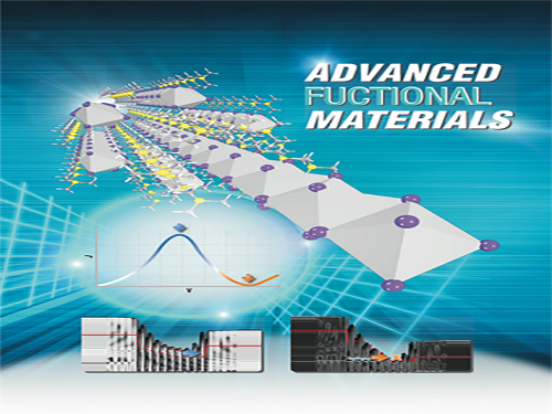 Novel Material Properties of Hybrid Perovskite Nanostructures for Next-generation Non-linear Electronic Devices
(from left: Juho Lee, Dr. Muhammad Ejaz Khan and Professor Yong-Hoon Kim)
A KAIST research team reported a novel non-linear device with the founding property coming from perovskite nanowires. They showed that hybrid perovskite-derived, inorganic-framework nanowires can acquire semi-metallicity, and proposed negative differential resistance (NDR) devices with excellent NDR characteristics that resulted from a novel quantum-hybridization NDR mechanism, implying the potential of perovskite nanowires to be realized in next-generation electronic devices.
Organic-inorganic hybrid halide perovskites have recently emerged as prominent candidates for photonic applications due to their excellent optoelectronic properties as well as their low cost and facile synthesis processes. Prominent progresses have been already made for devices including solar cells, light-emitting diodes, lasers and photodetectors.
However, research on electronic devices based on hybrid halide perovskites has not been actively pursued compared with their photonic device counterparts.
Professor Yong-Hoon Kim from the School of Electrical Engineering and his team took a closer look at low-dimensional organic-inorganic halide perovskite materials, which have enhanced quantum confinement effects, and particularly focused on the recently synthesized trimethylsulfonium (TMS) lead triiodide (CH3)3SPbI3.
Using supercomputer simulations, the team first showed that stripping the (CH3)3S or TMS organic ligands from the TMS PbI3 perovskite nanowires results in semi-metallic PbI3 columns, which contradicts the conventional assumption of the semiconducting or insulating characteristics of the inorganic perovskite framework.
Utilizing the semi-metallic PbI3 inorganic framework as the electrode, the team designed a tunneling junction device from perovskite nanowires and found that they exhibit excellent nonlinear negative differential resistance (NDR) behavior. The NDR property is a key to realizing next-generation, ultra-low-power, and multivalued non-linear devices. Furthermore, the team found that this NDR originates from a novel mechanism that involves the quantum-mechanical hybridization between channel and electrode states.
Professor Kim said, “This research demonstrates the potential of quantum mechanics-based computer simulations to lead developments in advanced nanomaterials and nanodevices. In particular, this research proposes a new direction in the development of a quantum mechanical tunneling device, which was the topic for which the Nobel Laureate in Physics in 1973 was awarded to Dr. Leo Esaki.
This research, led by Dr. Muhammad Ejaz Khan and PhD candidate Juho Lee, was published online in Advanced Functional Materials (10.1002/adfm.201807620) on January 7, 2019.
Figure. The draft version of the cover page of 'Advanced Functional Materials'
2019.02.22 View 7818
Novel Material Properties of Hybrid Perovskite Nanostructures for Next-generation Non-linear Electronic Devices
(from left: Juho Lee, Dr. Muhammad Ejaz Khan and Professor Yong-Hoon Kim)
A KAIST research team reported a novel non-linear device with the founding property coming from perovskite nanowires. They showed that hybrid perovskite-derived, inorganic-framework nanowires can acquire semi-metallicity, and proposed negative differential resistance (NDR) devices with excellent NDR characteristics that resulted from a novel quantum-hybridization NDR mechanism, implying the potential of perovskite nanowires to be realized in next-generation electronic devices.
Organic-inorganic hybrid halide perovskites have recently emerged as prominent candidates for photonic applications due to their excellent optoelectronic properties as well as their low cost and facile synthesis processes. Prominent progresses have been already made for devices including solar cells, light-emitting diodes, lasers and photodetectors.
However, research on electronic devices based on hybrid halide perovskites has not been actively pursued compared with their photonic device counterparts.
Professor Yong-Hoon Kim from the School of Electrical Engineering and his team took a closer look at low-dimensional organic-inorganic halide perovskite materials, which have enhanced quantum confinement effects, and particularly focused on the recently synthesized trimethylsulfonium (TMS) lead triiodide (CH3)3SPbI3.
Using supercomputer simulations, the team first showed that stripping the (CH3)3S or TMS organic ligands from the TMS PbI3 perovskite nanowires results in semi-metallic PbI3 columns, which contradicts the conventional assumption of the semiconducting or insulating characteristics of the inorganic perovskite framework.
Utilizing the semi-metallic PbI3 inorganic framework as the electrode, the team designed a tunneling junction device from perovskite nanowires and found that they exhibit excellent nonlinear negative differential resistance (NDR) behavior. The NDR property is a key to realizing next-generation, ultra-low-power, and multivalued non-linear devices. Furthermore, the team found that this NDR originates from a novel mechanism that involves the quantum-mechanical hybridization between channel and electrode states.
Professor Kim said, “This research demonstrates the potential of quantum mechanics-based computer simulations to lead developments in advanced nanomaterials and nanodevices. In particular, this research proposes a new direction in the development of a quantum mechanical tunneling device, which was the topic for which the Nobel Laureate in Physics in 1973 was awarded to Dr. Leo Esaki.
This research, led by Dr. Muhammad Ejaz Khan and PhD candidate Juho Lee, was published online in Advanced Functional Materials (10.1002/adfm.201807620) on January 7, 2019.
Figure. The draft version of the cover page of 'Advanced Functional Materials'
2019.02.22 View 7818 -
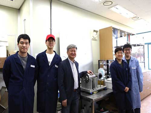 Highly Scalable Process to Obtain Stable 2D Nanosheet Dispersion
(Professor Do Hyun Kim and his team)
A KAIST team developed technology that allows the mass production of two-dimensional (2D) nanomaterial dispersion by utilizing the characteristic shearing force of hydraulic power.
The 2D nanosheet dispersion can be directly applied to solution-based processes to manufacture devices for electronics as well as energy storage and conversion. It is expected to be used in these devices with improved performance.
There have been numerous researches on the mass production of various 2D nanomaterial because they show outstanding physical and chemical characteristics when they are truly 2D.
With strong mechanical force or chemical reaction only, each existing exfoliation method has its limitation to make 2D material when the scale of manufacturing increases. They also face the issues of high cost and long process time.
Moreover, 2D nanosheets by the exfoliation have the tendency of agglomeration due to the surface energy. Usually, organic solvent or surfactant is required to obtain high yield and concentration of 2D material by minimizing agglomeration.
After several years of research, Professor Do Hyun Kim in the Department of Chemical and Biomolecular Engineering and his team verified that optimized shearing in their reactor provided the highest efficiency for the exfoliation of nanomaterial. For the increased reactor capacity, they selected a flow and a dispersive agent to develop a high-speed, mass-production process to get 2D nanosheets by physical exfoliation with an aqueous solution.
The team proposed a flow reactor based on Taylor-Couette flow, which has the advantage of high shear rate and mixing efficiency even under large reactor capacity.
In this research, Professor Young-Kyu Han at Dongguk University-Seoul carried out the Ab initio calculation to select the dispersive agent. According to his calculation, an ionic liquid can stabilize and disperse 2D nanomaterial even in a small concentration. This calculation could maximize the exfoliating efficiency.
Professor Bong Gill Choi at Kangwon National University carried out the evaluation of device made of resulting dispersion. The team used a membrane filtration process to make a flexible and highly conductive film of 2D material. The film was then applied to produce an electrode for the supercapacitor device with very high capacity per volume. They also confirmed its stability in their supercapacitor device.
Additionally, they applied dispersive nanomaterials including graphene, molybdenum disulfide (MoS₂), and boron nitride (BN) to inkjet printer ink and realized micrometer-thick nanomaterial patterns on A4 paper. The graphene ink showed no loss of electrical property after printing without additional heat treatment.
Professor Kim said, “This new technology for the high-speed mass production of nanomaterials can easily be applied to various 2D nanomaterials. It will accelerate the production of highly efficient devices for optoelectronics, biosensors, and energy storage/conversion units with low cost.”
This research, led by Dr. Jae-Min Jeong, was published in Advanced Functional Materials on August 12.
Figure 1. The cover page of Advanced Functional Materials
2018.12.19 View 6338
Highly Scalable Process to Obtain Stable 2D Nanosheet Dispersion
(Professor Do Hyun Kim and his team)
A KAIST team developed technology that allows the mass production of two-dimensional (2D) nanomaterial dispersion by utilizing the characteristic shearing force of hydraulic power.
The 2D nanosheet dispersion can be directly applied to solution-based processes to manufacture devices for electronics as well as energy storage and conversion. It is expected to be used in these devices with improved performance.
There have been numerous researches on the mass production of various 2D nanomaterial because they show outstanding physical and chemical characteristics when they are truly 2D.
With strong mechanical force or chemical reaction only, each existing exfoliation method has its limitation to make 2D material when the scale of manufacturing increases. They also face the issues of high cost and long process time.
Moreover, 2D nanosheets by the exfoliation have the tendency of agglomeration due to the surface energy. Usually, organic solvent or surfactant is required to obtain high yield and concentration of 2D material by minimizing agglomeration.
After several years of research, Professor Do Hyun Kim in the Department of Chemical and Biomolecular Engineering and his team verified that optimized shearing in their reactor provided the highest efficiency for the exfoliation of nanomaterial. For the increased reactor capacity, they selected a flow and a dispersive agent to develop a high-speed, mass-production process to get 2D nanosheets by physical exfoliation with an aqueous solution.
The team proposed a flow reactor based on Taylor-Couette flow, which has the advantage of high shear rate and mixing efficiency even under large reactor capacity.
In this research, Professor Young-Kyu Han at Dongguk University-Seoul carried out the Ab initio calculation to select the dispersive agent. According to his calculation, an ionic liquid can stabilize and disperse 2D nanomaterial even in a small concentration. This calculation could maximize the exfoliating efficiency.
Professor Bong Gill Choi at Kangwon National University carried out the evaluation of device made of resulting dispersion. The team used a membrane filtration process to make a flexible and highly conductive film of 2D material. The film was then applied to produce an electrode for the supercapacitor device with very high capacity per volume. They also confirmed its stability in their supercapacitor device.
Additionally, they applied dispersive nanomaterials including graphene, molybdenum disulfide (MoS₂), and boron nitride (BN) to inkjet printer ink and realized micrometer-thick nanomaterial patterns on A4 paper. The graphene ink showed no loss of electrical property after printing without additional heat treatment.
Professor Kim said, “This new technology for the high-speed mass production of nanomaterials can easily be applied to various 2D nanomaterials. It will accelerate the production of highly efficient devices for optoelectronics, biosensors, and energy storage/conversion units with low cost.”
This research, led by Dr. Jae-Min Jeong, was published in Advanced Functional Materials on August 12.
Figure 1. The cover page of Advanced Functional Materials
2018.12.19 View 6338 -
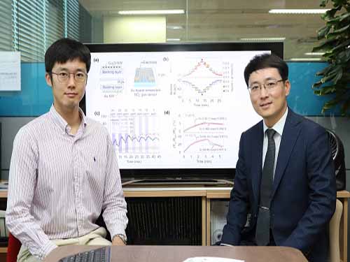 Transfering Nanowires onto a Flexible Substrate
(from left: PhD Min-Ho Seo and Professor Jun-Bo Yoon)
Boasting excellent physical and chemical properties, nanowires (NWs) are suitable for fabricating flexible electronics; therefore, technology to transfer well-aligned wires plays a crucial role in enhancing performance of the devices. A KAIST research team succeeded in developing NW-transfer technology that is expected to enhance the existing chemical reaction-based NW fabrication technology that has this far showed low performance in applicability and productivity.
NWs, one of the most well-known nanomaterials, have the structural advantage of being small and lightweight. Hence, NW-transfer technology has drawn attention because it can fabricate high-performance, flexible nanodevices with high simplicity and throughput.
A conventional nanowire-fabrication method generally has an irregularity issue since it mixes chemically synthesized nanowires in a solution and randomly distributes the NWs onto flexible substrates. Hence, numerous nanofabrication processes have emerged, and one of them is master-mold-based, which enables the fabrication of highly ordered NW arrays embedded onto substrates in a simple and cost-effective manner, but its employment is limited to only some materials because of its chemistry-based NW-transfer mechanism, which is complex and time consuming. For the successful transfer, it requires that adequate chemicals controlling the chemical interfacial adhesion between the master mold, NWs, and flexible substrate be present.
Here, Professor Jun-Bo Yoon and his team from the School of Electrical Engineering introduced a material-independent mechanical-interlocking-based nanowire-transfer (MINT) method to fabricate ultralong and fully aligned NWs on a large flexible substrate in a highly robust manner.
This method involves sequentially forming a nanosacrificial layer and NWs on a nanograting substrate that becomes the master mold for the transfer, then weakening the structure of the nanosacrificial layer through a dry etching process. The nanosacrificial layer very weakly holds the nanowires on the master mold. Therefore, when using a flexible substrate material, the nanowires are very easily transferred from the master mold to the substrate, just like a piece of tape lifting dust off a carpet.
This technology uses common physical vapor deposition and does not rely on NW materials, making it easy to fabricate NWs onto the flexible substrates.
Using this technology, the team was able to fabricate a variety of metal and metal-oxide NWs, including gold, platinum, and copper – all perfectly aligned on a flexible substrate. They also confirmed that it can be applied to creating stable and applicable devices in everyday life by successfully applying it to flexible heaters and gas sensors.
PhD Min-Ho Seo who led this research said, “We have successfully aligned various metals and semiconductor NWs with excellent physical properties onto flexible substrates and applied them to fabricated devices. As a platform-technology, it will contribute to developing high-performing and stable electronic devices.”
This research was published in ACS Nano on May 24.
Figure 1. Photograph of the fabricated wafer-scale fully aligned and ultralong Au nanowire array on a flexible substrate
2018.09.17 View 6755
Transfering Nanowires onto a Flexible Substrate
(from left: PhD Min-Ho Seo and Professor Jun-Bo Yoon)
Boasting excellent physical and chemical properties, nanowires (NWs) are suitable for fabricating flexible electronics; therefore, technology to transfer well-aligned wires plays a crucial role in enhancing performance of the devices. A KAIST research team succeeded in developing NW-transfer technology that is expected to enhance the existing chemical reaction-based NW fabrication technology that has this far showed low performance in applicability and productivity.
NWs, one of the most well-known nanomaterials, have the structural advantage of being small and lightweight. Hence, NW-transfer technology has drawn attention because it can fabricate high-performance, flexible nanodevices with high simplicity and throughput.
A conventional nanowire-fabrication method generally has an irregularity issue since it mixes chemically synthesized nanowires in a solution and randomly distributes the NWs onto flexible substrates. Hence, numerous nanofabrication processes have emerged, and one of them is master-mold-based, which enables the fabrication of highly ordered NW arrays embedded onto substrates in a simple and cost-effective manner, but its employment is limited to only some materials because of its chemistry-based NW-transfer mechanism, which is complex and time consuming. For the successful transfer, it requires that adequate chemicals controlling the chemical interfacial adhesion between the master mold, NWs, and flexible substrate be present.
Here, Professor Jun-Bo Yoon and his team from the School of Electrical Engineering introduced a material-independent mechanical-interlocking-based nanowire-transfer (MINT) method to fabricate ultralong and fully aligned NWs on a large flexible substrate in a highly robust manner.
This method involves sequentially forming a nanosacrificial layer and NWs on a nanograting substrate that becomes the master mold for the transfer, then weakening the structure of the nanosacrificial layer through a dry etching process. The nanosacrificial layer very weakly holds the nanowires on the master mold. Therefore, when using a flexible substrate material, the nanowires are very easily transferred from the master mold to the substrate, just like a piece of tape lifting dust off a carpet.
This technology uses common physical vapor deposition and does not rely on NW materials, making it easy to fabricate NWs onto the flexible substrates.
Using this technology, the team was able to fabricate a variety of metal and metal-oxide NWs, including gold, platinum, and copper – all perfectly aligned on a flexible substrate. They also confirmed that it can be applied to creating stable and applicable devices in everyday life by successfully applying it to flexible heaters and gas sensors.
PhD Min-Ho Seo who led this research said, “We have successfully aligned various metals and semiconductor NWs with excellent physical properties onto flexible substrates and applied them to fabricated devices. As a platform-technology, it will contribute to developing high-performing and stable electronic devices.”
This research was published in ACS Nano on May 24.
Figure 1. Photograph of the fabricated wafer-scale fully aligned and ultralong Au nanowire array on a flexible substrate
2018.09.17 View 6755 -
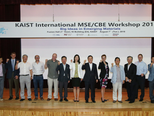 The MSE/CBE Int'l Workshop Explores Big Ideas in Emerging Materials
(KAIST President Sung-Chul Shin with scholars participated in the workshop)
The MSE/CBE International Workshop brought together editors from key academic journals in multidisciplinary materials science and scholars from leading universities at KAIST on Aug. 7.
The workshop hosted ten distinguished speakers in the fields of nanostructures for next-generation emerging applications, chemical and bio-engineering, and materials innovation for functional applications. They explored opportunities and challenges for reinventing novel materials that will solve complex problems.
(From left: Professor Buriak, Professor Swager and Professor Il-Doo Kim)
Speakers included: Chief Editor of Nature Materials Vincent Dusastre; Editor-in- Chief of ACS NANO and professor at UCLA Paul S. Weiss; Jillian M. Buriak, Editor-in-Chief of Chemistry of Materials; Associate Editor of Macromolecules and professor at MIT Timothy M. Swager; Coordinating Editor of Acta Materialia and Head of the Department of Materials Science and Engineering at MIT Christopher A. Schuh; Editor-in-Chief of Biotechnology Journal and Metabolic Engineering and Distinguished Professor at KAIST Sang-Yup Lee; Associate Editor of Energy Storage Materials and professor at KAIST Sang Ouk Kim; Professor Jeffrey C. Grossman at MIT; Professor Zhenan Bao at Stanford University; and Professor Hyuck Mo Lee, head of the Department of Materials Science and Engineering at KAIST.
Interdisciplinary materials research holds the key to building technological competitiveness in many industrial sectors extending from energy, environment, and health care to medicine and beyond. It has also been the bedrock of KAIST’s scholarship and research innovation. More than 200 faculty members in the field of materials science produce about 800 SCI papers every year. The two departments of materials science and chemical biomolecular engineering are leading KAIST’s global reputation, as they were both ranked 13th and 14th in the QS World University Ranking by Subject this year.
(Professor Il-Doo Kim fromt he Department of Materials Science Engineering)
Professor Il-Doo Kim from the Department of Materials Science Engineering has been the chair of this workshop from 2016. In hosting the second one this year, he said that he hopes this year’s workshop will inspire many materials scientists to have big ideas and work to make those big ideas get noticed in order to have a real impact.
(KAIST President Sung-Chul Shin)
President Sung-Chul Shin, who is a physicist specializing in materials physics, expressed his keen interest in the workshop, saying innovative materials made of unthinkable and noble combinations will be the key factor in determining the competitiveness of new technology and new industries. He lauded international collaborations for making new materials and the scholarly passion to evaluate the materials’ characteristics that made this significant progress possible.
Dr. Vincent Dusastre, chief editor of Nature Materials, presented recent trends in materials for energy. He described how the rational design and improvement of materials’ properties can lead to energy alternatives which will compete with existing technologies. He pointed out that given the dramatic fundamental and practical breakthroughs that are taking place in the realization of solar cells with high energy-conversion efficiency, the improvement of batteries for electric vehicles and the grid is also a major challenge. He stressed, “Key advances in sustainable approaches beyond Li-ion batteries and control of redox processes are also greatly needed.”
Meanwhile, ACS NANO Editor-in-Chief Paul S. Weiss spoke on the importance of heterogeneity in the structure and function of molecules and nanoscale assemblies. He stressed that such extensiveness of multi-interdisciplinary research will accelerate a greater impact as indicated when the fields of neuroscience and microbiome converged with nanoscience and nanotechnology.
Editor-in-Chief of Chemistry of Materials Professor Jillian M. Buriak from the University of Alberta described how predictive models and machine learning can replace time consuming empirical device production and screening. By understanding and pinpointing the frustrating bottlenecks in the design of stable and efficient organic photovoltaics, much faster throughput can be obtained to enable a more direct pathway to stability, efficiency, and finally commercialization.
2018.08.13 View 13893
The MSE/CBE Int'l Workshop Explores Big Ideas in Emerging Materials
(KAIST President Sung-Chul Shin with scholars participated in the workshop)
The MSE/CBE International Workshop brought together editors from key academic journals in multidisciplinary materials science and scholars from leading universities at KAIST on Aug. 7.
The workshop hosted ten distinguished speakers in the fields of nanostructures for next-generation emerging applications, chemical and bio-engineering, and materials innovation for functional applications. They explored opportunities and challenges for reinventing novel materials that will solve complex problems.
(From left: Professor Buriak, Professor Swager and Professor Il-Doo Kim)
Speakers included: Chief Editor of Nature Materials Vincent Dusastre; Editor-in- Chief of ACS NANO and professor at UCLA Paul S. Weiss; Jillian M. Buriak, Editor-in-Chief of Chemistry of Materials; Associate Editor of Macromolecules and professor at MIT Timothy M. Swager; Coordinating Editor of Acta Materialia and Head of the Department of Materials Science and Engineering at MIT Christopher A. Schuh; Editor-in-Chief of Biotechnology Journal and Metabolic Engineering and Distinguished Professor at KAIST Sang-Yup Lee; Associate Editor of Energy Storage Materials and professor at KAIST Sang Ouk Kim; Professor Jeffrey C. Grossman at MIT; Professor Zhenan Bao at Stanford University; and Professor Hyuck Mo Lee, head of the Department of Materials Science and Engineering at KAIST.
Interdisciplinary materials research holds the key to building technological competitiveness in many industrial sectors extending from energy, environment, and health care to medicine and beyond. It has also been the bedrock of KAIST’s scholarship and research innovation. More than 200 faculty members in the field of materials science produce about 800 SCI papers every year. The two departments of materials science and chemical biomolecular engineering are leading KAIST’s global reputation, as they were both ranked 13th and 14th in the QS World University Ranking by Subject this year.
(Professor Il-Doo Kim fromt he Department of Materials Science Engineering)
Professor Il-Doo Kim from the Department of Materials Science Engineering has been the chair of this workshop from 2016. In hosting the second one this year, he said that he hopes this year’s workshop will inspire many materials scientists to have big ideas and work to make those big ideas get noticed in order to have a real impact.
(KAIST President Sung-Chul Shin)
President Sung-Chul Shin, who is a physicist specializing in materials physics, expressed his keen interest in the workshop, saying innovative materials made of unthinkable and noble combinations will be the key factor in determining the competitiveness of new technology and new industries. He lauded international collaborations for making new materials and the scholarly passion to evaluate the materials’ characteristics that made this significant progress possible.
Dr. Vincent Dusastre, chief editor of Nature Materials, presented recent trends in materials for energy. He described how the rational design and improvement of materials’ properties can lead to energy alternatives which will compete with existing technologies. He pointed out that given the dramatic fundamental and practical breakthroughs that are taking place in the realization of solar cells with high energy-conversion efficiency, the improvement of batteries for electric vehicles and the grid is also a major challenge. He stressed, “Key advances in sustainable approaches beyond Li-ion batteries and control of redox processes are also greatly needed.”
Meanwhile, ACS NANO Editor-in-Chief Paul S. Weiss spoke on the importance of heterogeneity in the structure and function of molecules and nanoscale assemblies. He stressed that such extensiveness of multi-interdisciplinary research will accelerate a greater impact as indicated when the fields of neuroscience and microbiome converged with nanoscience and nanotechnology.
Editor-in-Chief of Chemistry of Materials Professor Jillian M. Buriak from the University of Alberta described how predictive models and machine learning can replace time consuming empirical device production and screening. By understanding and pinpointing the frustrating bottlenecks in the design of stable and efficient organic photovoltaics, much faster throughput can be obtained to enable a more direct pathway to stability, efficiency, and finally commercialization.
2018.08.13 View 13893 -
 The 8th KINC Fusion Research Awardees
The KAIST Institute for NanoCentury held the 8th KINC Fusion Research Award in order to encourage professors’ convergence studies and instill students’ willingness to research. The award ceremony took place in the KI Building at KAIST on March 13.
The KINC Fusion Research Award selects the most outstanding convergence studies among research undertaken last year, and awards researchers who participated in that research.
The 8th KINC Fusion Research Award went to Professor Yoon Sung Nam from the Department of Materials Science and Engineering and Professor Inkyu Park from the Department of Mechanical Engineering. Their research reported the spontaneous self-biomineralization of palladium (Pd) ions on a filamentous virus to form ligand-free Pd nanowires without reducing reagents or using additional surface stabilizers (Title: Virus-Templated Self-Mineralization of Ligand-Free Colloidal Palladium Nanostructures for High Surface Activity and Stability, Advanced Functional Materials (2017)).
Professor Hee-Tae Jung, the Director of KAIST Institute for the NanoCentury and the host of the KINC Fusion Research Award said, “Convergence will be the crucial keyword that will lead to revolutionary change. Hence, the importance of convergence study should be improved. We will put every effort into creating a research environment for increasing convergence study.
The KAIST Institute for the NanoCentury was established in June 2006 under the KAIST Institute with a mission of creating convergence study by tearing down boarders among departments and carrying out interdisciplinary joint research. Currently, approximately 90 professors from 14 departments participate the institute. It aims to become a hub of university institutes for nano-fusion research.
2018.03.19 View 14236
The 8th KINC Fusion Research Awardees
The KAIST Institute for NanoCentury held the 8th KINC Fusion Research Award in order to encourage professors’ convergence studies and instill students’ willingness to research. The award ceremony took place in the KI Building at KAIST on March 13.
The KINC Fusion Research Award selects the most outstanding convergence studies among research undertaken last year, and awards researchers who participated in that research.
The 8th KINC Fusion Research Award went to Professor Yoon Sung Nam from the Department of Materials Science and Engineering and Professor Inkyu Park from the Department of Mechanical Engineering. Their research reported the spontaneous self-biomineralization of palladium (Pd) ions on a filamentous virus to form ligand-free Pd nanowires without reducing reagents or using additional surface stabilizers (Title: Virus-Templated Self-Mineralization of Ligand-Free Colloidal Palladium Nanostructures for High Surface Activity and Stability, Advanced Functional Materials (2017)).
Professor Hee-Tae Jung, the Director of KAIST Institute for the NanoCentury and the host of the KINC Fusion Research Award said, “Convergence will be the crucial keyword that will lead to revolutionary change. Hence, the importance of convergence study should be improved. We will put every effort into creating a research environment for increasing convergence study.
The KAIST Institute for the NanoCentury was established in June 2006 under the KAIST Institute with a mission of creating convergence study by tearing down boarders among departments and carrying out interdisciplinary joint research. Currently, approximately 90 professors from 14 departments participate the institute. It aims to become a hub of university institutes for nano-fusion research.
2018.03.19 View 14236