electron
-
 Black Phosphorous Tunnel Field-Effect Transistor as an Alternative Ultra-low Power Switch
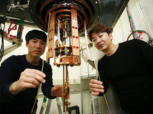
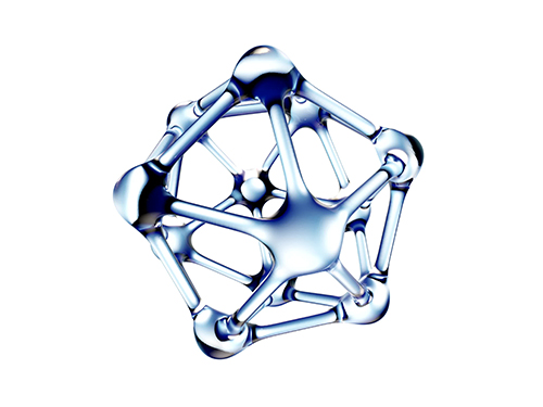
Researchers have reported a black phosphorus transistor that can be used as an alternative ultra-low power switch. A research team led by Professor Sungjae Cho in the KAIST Department of Physics developed a thickness-controlled black phosphorous tunnel field-effect transistor (TFET) that shows 10-times lower switching power consumption as well as 10,000-times lower standby power consumption than conventional complementary metal-oxide-semiconductor (CMOS) transistors.
The research team said they developed fast and low-power transistors that can replace conventional CMOS transistors. In particular, they solved problems that have degraded TFET operation speed and performance, paving the way to extend Moore’s Law.
In the study featured in Nature Nanotechnology last month, Professor Cho’s team reported a natural heterojunction TFET with spatially varying layer thickness in black phosphorous without interface problems. They achieved record-low average subthreshold swing values over 4-5 dec of current and record-high, on-state current, which allows the TFETs to operate as fast as conventional CMOS transistors with as much lower power consumption.
"We successfully developed the first transistor that achieved the essential criteria for fast, low-power switching. Our newly developed TFETs can replace CMOS transistors by solving a major issue regarding the performance degradation of TFETs,"Professor Cho said.
The continuous down-scaling of transistors has been the key to the successful development of current information technology. However, with Moore’s Law reaching its limits due to the increased power consumption, the development of new alternative transistor designs has emerged as an urgent need.
Reducing both switching and standby power consumption while further scaling transistors requires overcoming the thermionic limit of subthreshold swing, which is defined as the required voltage per ten-fold current increase in the subthreshold region. In order to reduce both the switching and standby power of CMOS circuits, it is critical to reduce the subthreshold swing of the transistors.
However, there is fundamental subthreshold swing limit of 60 mV/dec in CMOS transistors, which originates from thermal carrier injection. The International Roadmap for Devices and Systems has already predicted that new device geometries with new materials beyond CMOS will be required to address transistor scaling challenges in the near future. In particular, TFETs have been suggested as a major alternative to CMOS transistors, since the subthreshold swing in TFETs can be substantially reduced below the thermionic limit of 60 mV/dec. TFETs operate via quantum tunneling, which does not limit subthreshold swing as in thermal injection of CMOS transistors.
In particular, heterojunction TFETs hold significant promise for delivering both low subthreshold swing and high on-state current. High on-current is essential for the fast operation of transistors since charging a device to on state takes a longer time with lower currents. Unlike theoretical expectations, previously developed heterojunction TFETs show 100-100,000x lower on-state current (100-100,000x slower operation speeds) than CMOS transistors due to interface problems in the heterojunction. This low operation speed impedes the replacement of CMOS transistors with low-power TFETs.
Professor Cho said, “We have demonstrated for the first time, to the best of our knowledge, TFET optimization for both fast and ultra-low-power operations, which is essential to replace CMOS transistors for low-power applications.” He said he is very delighted to extend Moore’s Law, which may eventually affect almost every aspect of life and society. This study (https://doi.org/10.1038/s41565-019-0623-7) was supported by the National Research Foundation of Korea.
Publication:
Kim et al. (2020) Thickness-controlled black phosphorus tunnel field-effect transistor for low-power switches. Nature Nanotechnology. Available online at https://doi.org/10.1038/s41565-019-0623-7
Profile:
Professor Sungjae Cho
sungjae.cho@kaist.ac.kr
Department of Physics
http://qtak.kaist.ac.kr/
KAIST
Profile:
Seungho Kim, PhD Candidate
krksh21@kaist.ac.kr
Department of Physics
http://qtak.kaist.ac.kr/
KAIST
(END)
2020.02.21 View 14249
Black Phosphorous Tunnel Field-Effect Transistor as an Alternative Ultra-low Power Switch
Researchers have reported a black phosphorus transistor that can be used as an alternative ultra-low power switch. A research team led by Professor Sungjae Cho in the KAIST Department of Physics developed a thickness-controlled black phosphorous tunnel field-effect transistor (TFET) that shows 10-times lower switching power consumption as well as 10,000-times lower standby power consumption than conventional complementary metal-oxide-semiconductor (CMOS) transistors.
The research team said they developed fast and low-power transistors that can replace conventional CMOS transistors. In particular, they solved problems that have degraded TFET operation speed and performance, paving the way to extend Moore’s Law.
In the study featured in Nature Nanotechnology last month, Professor Cho’s team reported a natural heterojunction TFET with spatially varying layer thickness in black phosphorous without interface problems. They achieved record-low average subthreshold swing values over 4-5 dec of current and record-high, on-state current, which allows the TFETs to operate as fast as conventional CMOS transistors with as much lower power consumption.
"We successfully developed the first transistor that achieved the essential criteria for fast, low-power switching. Our newly developed TFETs can replace CMOS transistors by solving a major issue regarding the performance degradation of TFETs,"Professor Cho said.
The continuous down-scaling of transistors has been the key to the successful development of current information technology. However, with Moore’s Law reaching its limits due to the increased power consumption, the development of new alternative transistor designs has emerged as an urgent need.
Reducing both switching and standby power consumption while further scaling transistors requires overcoming the thermionic limit of subthreshold swing, which is defined as the required voltage per ten-fold current increase in the subthreshold region. In order to reduce both the switching and standby power of CMOS circuits, it is critical to reduce the subthreshold swing of the transistors.
However, there is fundamental subthreshold swing limit of 60 mV/dec in CMOS transistors, which originates from thermal carrier injection. The International Roadmap for Devices and Systems has already predicted that new device geometries with new materials beyond CMOS will be required to address transistor scaling challenges in the near future. In particular, TFETs have been suggested as a major alternative to CMOS transistors, since the subthreshold swing in TFETs can be substantially reduced below the thermionic limit of 60 mV/dec. TFETs operate via quantum tunneling, which does not limit subthreshold swing as in thermal injection of CMOS transistors.
In particular, heterojunction TFETs hold significant promise for delivering both low subthreshold swing and high on-state current. High on-current is essential for the fast operation of transistors since charging a device to on state takes a longer time with lower currents. Unlike theoretical expectations, previously developed heterojunction TFETs show 100-100,000x lower on-state current (100-100,000x slower operation speeds) than CMOS transistors due to interface problems in the heterojunction. This low operation speed impedes the replacement of CMOS transistors with low-power TFETs.
Professor Cho said, “We have demonstrated for the first time, to the best of our knowledge, TFET optimization for both fast and ultra-low-power operations, which is essential to replace CMOS transistors for low-power applications.” He said he is very delighted to extend Moore’s Law, which may eventually affect almost every aspect of life and society. This study (https://doi.org/10.1038/s41565-019-0623-7) was supported by the National Research Foundation of Korea.
Publication:
Kim et al. (2020) Thickness-controlled black phosphorus tunnel field-effect transistor for low-power switches. Nature Nanotechnology. Available online at https://doi.org/10.1038/s41565-019-0623-7
Profile:
Professor Sungjae Cho
sungjae.cho@kaist.ac.kr
Department of Physics
http://qtak.kaist.ac.kr/
KAIST
Profile:
Seungho Kim, PhD Candidate
krksh21@kaist.ac.kr
Department of Physics
http://qtak.kaist.ac.kr/
KAIST
(END)
2020.02.21 View 14249 -
 New Graphene-Based Metasurface Capable of Independent Amplitude and Phase Control of Light
Researchers described a new strategy of designing metamolecules that incorporates two independently controllable subwavelength meta-atoms. This two-parametric control of the metamolecule secures the complete control of both amplitude and the phase of light.
A KAIST research team in collaboration with the University of Wisconsin-Madison theoretically suggested a graphene-based active metasurface capable of independent amplitude and phase control of mid-infrared light. This research gives a new insight into modulating the mid-infrared wavefront with high resolution by solving the problem of the independent control of light amplitude and phase, which has remained a long-standing challenge.
Light modulation technology is essential for developing future optical devices such as holography, high-resolution imaging, and optical communication systems. Liquid crystals and a microelectromechanical system (MEMS) have previously been utilized to modulate light. However, both methods suffer from significantly limited driving speeds and unit pixel sizes larger than the diffraction limit, which consequently prevent their integration into photonic systems.
The metasurface platform is considered a strong candidate for the next generation of light modulation technology. Metasurfaces have optical properties that natural materials cannot have, and can overcome the limitations of conventional optical systems, such as forming a high-resolution image beyond the diffraction limit. In particular, the active metasurface is regarded as a technology with a wide range of applications due to its tunable optical characteristics with an electrical signal.
However, the previous active metasurfaces suffered from the inevitable correlation between light amplitude control and phase control. This problem is caused by the modulation mechanism of conventional metasurfaces. Conventional metasurfaces have been designed such that a metaatom only has one resonance condition, but a single resonant design inherently lacks the degrees of freedom to independently control the amplitude and phase of light.
The research team made a metaunit by combining two independently controllable metaatoms, dramatically improving the modulation range of active metasurfaces. The proposed metasurface can control the amplitude and phase of the mid-infrared light independently with a resolution beyond the diffraction limit, thus allowing complete control of the optical wavefront.
The research team theoretically confirmed the performance of the proposed active metasurface and the possibility of wavefront shaping using this design method. Furthermore, they developed an analytical method that can approximate the optical properties of metasurfaces without complex electromagnetic simulations. This analytical platform proposes a more intuitive and comprehensively applicable metasurface design guideline.
The proposed technology is expected to enable accurate wavefront shaping with a much higher spatial resolution than existing wavefront shaping technologies, which will be applied to active optical systems such as mid-infrared holography, high-speed beam steering devices that can be applied for LiDAR, and variable focus infrared lenses.
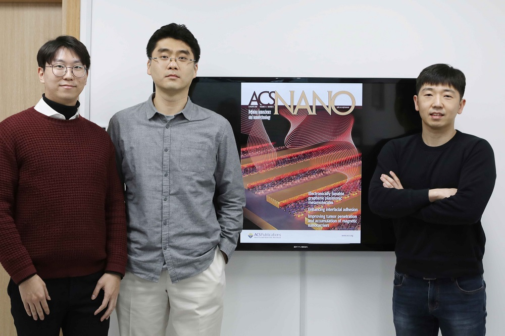
Professor Min Seok Jang commented, "This study showed the independent control amplitude and phase of light, which has been a long-standing quest in light modulator technology. The development of optical devices using complex wavefront control is expected to become more active in the future."
MS candidate Sangjun Han and Dr. Seyoon Kim of the University of Wisconsin-Madison are the co-first authors of the research, which was published and selected as the front cover of the January 28 edition of ACS Nano titled “Complete complex amplitude modulation with electronically tunable graphene plasmonic metamolecules.”
This research was funded by the Samsung Research Funding & Incubation Center for Future Technology.
Publication:
Han et al. (2020) Complete Complex Amplitude Modulation with Electronically Tunable Graphene Plasmonic Metamolecules. ACS Nano, Vol. 14, Issue 1, pp. 1166-1175. Available online at https://doi.org/10.1021/acsnano.9b09277
Profile: Prof. Min Seok Jang, MS, PhD
jang.minseok@kaist.ac.kr
http://jlab.kaist.ac.kr/
Associate Professor
Jang Research Group
School of Electrical Engineering
Korea Advanced Institute of Science and Technology (KAIST)
http://kaist.ac.kr
Daejeon, Republic of Korea
Profile: Sangjun Han
sangjun.han@kaist.ac.kr
MS Candidate
School of Electrical Engineering
Korea Advanced Institute of Science and Technology (KAIST)
http://kaist.ac.kr
Daejeon, Republic of Korea
(END)
2020.02.20 View 11022
New Graphene-Based Metasurface Capable of Independent Amplitude and Phase Control of Light
Researchers described a new strategy of designing metamolecules that incorporates two independently controllable subwavelength meta-atoms. This two-parametric control of the metamolecule secures the complete control of both amplitude and the phase of light.
A KAIST research team in collaboration with the University of Wisconsin-Madison theoretically suggested a graphene-based active metasurface capable of independent amplitude and phase control of mid-infrared light. This research gives a new insight into modulating the mid-infrared wavefront with high resolution by solving the problem of the independent control of light amplitude and phase, which has remained a long-standing challenge.
Light modulation technology is essential for developing future optical devices such as holography, high-resolution imaging, and optical communication systems. Liquid crystals and a microelectromechanical system (MEMS) have previously been utilized to modulate light. However, both methods suffer from significantly limited driving speeds and unit pixel sizes larger than the diffraction limit, which consequently prevent their integration into photonic systems.
The metasurface platform is considered a strong candidate for the next generation of light modulation technology. Metasurfaces have optical properties that natural materials cannot have, and can overcome the limitations of conventional optical systems, such as forming a high-resolution image beyond the diffraction limit. In particular, the active metasurface is regarded as a technology with a wide range of applications due to its tunable optical characteristics with an electrical signal.
However, the previous active metasurfaces suffered from the inevitable correlation between light amplitude control and phase control. This problem is caused by the modulation mechanism of conventional metasurfaces. Conventional metasurfaces have been designed such that a metaatom only has one resonance condition, but a single resonant design inherently lacks the degrees of freedom to independently control the amplitude and phase of light.
The research team made a metaunit by combining two independently controllable metaatoms, dramatically improving the modulation range of active metasurfaces. The proposed metasurface can control the amplitude and phase of the mid-infrared light independently with a resolution beyond the diffraction limit, thus allowing complete control of the optical wavefront.
The research team theoretically confirmed the performance of the proposed active metasurface and the possibility of wavefront shaping using this design method. Furthermore, they developed an analytical method that can approximate the optical properties of metasurfaces without complex electromagnetic simulations. This analytical platform proposes a more intuitive and comprehensively applicable metasurface design guideline.
The proposed technology is expected to enable accurate wavefront shaping with a much higher spatial resolution than existing wavefront shaping technologies, which will be applied to active optical systems such as mid-infrared holography, high-speed beam steering devices that can be applied for LiDAR, and variable focus infrared lenses.
Professor Min Seok Jang commented, "This study showed the independent control amplitude and phase of light, which has been a long-standing quest in light modulator technology. The development of optical devices using complex wavefront control is expected to become more active in the future."
MS candidate Sangjun Han and Dr. Seyoon Kim of the University of Wisconsin-Madison are the co-first authors of the research, which was published and selected as the front cover of the January 28 edition of ACS Nano titled “Complete complex amplitude modulation with electronically tunable graphene plasmonic metamolecules.”
This research was funded by the Samsung Research Funding & Incubation Center for Future Technology.
Publication:
Han et al. (2020) Complete Complex Amplitude Modulation with Electronically Tunable Graphene Plasmonic Metamolecules. ACS Nano, Vol. 14, Issue 1, pp. 1166-1175. Available online at https://doi.org/10.1021/acsnano.9b09277
Profile: Prof. Min Seok Jang, MS, PhD
jang.minseok@kaist.ac.kr
http://jlab.kaist.ac.kr/
Associate Professor
Jang Research Group
School of Electrical Engineering
Korea Advanced Institute of Science and Technology (KAIST)
http://kaist.ac.kr
Daejeon, Republic of Korea
Profile: Sangjun Han
sangjun.han@kaist.ac.kr
MS Candidate
School of Electrical Engineering
Korea Advanced Institute of Science and Technology (KAIST)
http://kaist.ac.kr
Daejeon, Republic of Korea
(END)
2020.02.20 View 11022 -
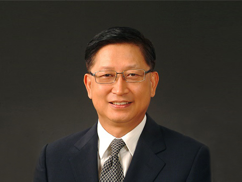 New KAA President Chilhee Chung Calls Alumni Engagement a Top Priority
The KAIST Alumni Association (KAA) inaugurated Advisor Chilhee Chung of Samsung Electronics as its new president. President Chung was preceded by Ki-Chul Cha, the CEO of Inbody Co. Ltd. His term as the 25th president starts from February 2020 and ends in January 2022.
President Chung received his master’s degree from KAIST's Department of Physics in 1979 and joined Samsung Electronics the same year. He also holds a doctorate in physics from Michigan State University in the United States.
President Chung devoted himself to helping Samsung Electronics and Korea's system semiconductor and memory device technologies achieve global dominance for more than 40 years. He led future technology development at Samsung Electronics in the fields of quantum dot and neural processing from various leadership positions, including the head of the Semiconductor R&D Center, and the president of Samsung Advanced Institute of Technology (SAIT).
President Chung is currently an advisor to SAIT, a member of the Presidential Advisory Council on Science and Technology (PACST), and the chairman of the 2045 National Future Strategy Committee and the Nano Technology Research Association (NTRA).
President Chung said, “KAIST, throughout its history of half a century, has been working tirelessly to become the world’s best, beyond being the best in Korea. We, the alumni of KAIST, have the commensurate duty as well as the privilege of being proud members of KAIST, as the university's global stature grows.”
“Recently, 46 alumni made 535 million won in donations, and established a scholarship to encourage entrepreneurial spirit in members of the KAIST community. This fund was dedicated to supporting 30 alumni entrepreneurs and students participating in the International Consumer Electronics Show (CES) 2020 that was held in Las Vegas last month. Moreover, another alumnus of ours Byeong-Gyu Chang, the CSO of the KRAFTON Inc., donated 10 billion won to KAIST in hopes of opening up more opportunities that may lead KAIST students to success. Mr. Chang’s donation is by far the largest that has been made by KAIST alumni. I feel grateful to see more alumni getting involved in shaping the future of KAIST these days, and my top priority as the new president of the KAA will be to stimulate the alumni association and engagement in the spirit of ‘Team KAIST’,” he added.
More than 900 alumni, including President Sung-Chul Shin who is also an alumnus of KAIST, gathered in Seoul on January 18 to celebrate the New Year and the newly-elected leadership of the KAA.
(END)
2020.02.03 View 9097
New KAA President Chilhee Chung Calls Alumni Engagement a Top Priority
The KAIST Alumni Association (KAA) inaugurated Advisor Chilhee Chung of Samsung Electronics as its new president. President Chung was preceded by Ki-Chul Cha, the CEO of Inbody Co. Ltd. His term as the 25th president starts from February 2020 and ends in January 2022.
President Chung received his master’s degree from KAIST's Department of Physics in 1979 and joined Samsung Electronics the same year. He also holds a doctorate in physics from Michigan State University in the United States.
President Chung devoted himself to helping Samsung Electronics and Korea's system semiconductor and memory device technologies achieve global dominance for more than 40 years. He led future technology development at Samsung Electronics in the fields of quantum dot and neural processing from various leadership positions, including the head of the Semiconductor R&D Center, and the president of Samsung Advanced Institute of Technology (SAIT).
President Chung is currently an advisor to SAIT, a member of the Presidential Advisory Council on Science and Technology (PACST), and the chairman of the 2045 National Future Strategy Committee and the Nano Technology Research Association (NTRA).
President Chung said, “KAIST, throughout its history of half a century, has been working tirelessly to become the world’s best, beyond being the best in Korea. We, the alumni of KAIST, have the commensurate duty as well as the privilege of being proud members of KAIST, as the university's global stature grows.”
“Recently, 46 alumni made 535 million won in donations, and established a scholarship to encourage entrepreneurial spirit in members of the KAIST community. This fund was dedicated to supporting 30 alumni entrepreneurs and students participating in the International Consumer Electronics Show (CES) 2020 that was held in Las Vegas last month. Moreover, another alumnus of ours Byeong-Gyu Chang, the CSO of the KRAFTON Inc., donated 10 billion won to KAIST in hopes of opening up more opportunities that may lead KAIST students to success. Mr. Chang’s donation is by far the largest that has been made by KAIST alumni. I feel grateful to see more alumni getting involved in shaping the future of KAIST these days, and my top priority as the new president of the KAA will be to stimulate the alumni association and engagement in the spirit of ‘Team KAIST’,” he added.
More than 900 alumni, including President Sung-Chul Shin who is also an alumnus of KAIST, gathered in Seoul on January 18 to celebrate the New Year and the newly-elected leadership of the KAA.
(END)
2020.02.03 View 9097 -
 KAIST Showcases Advanced Technologies at CES 2020
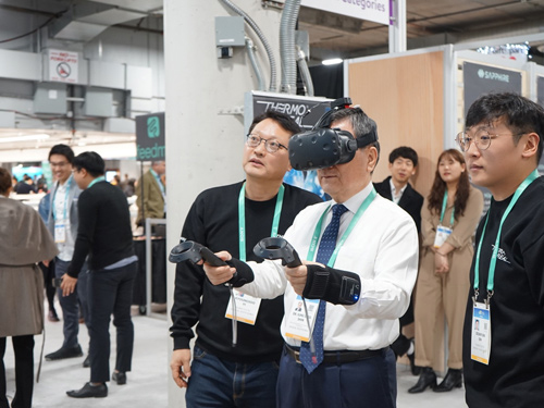
< President Sung-Chul Shin experiencing cooling gaming headset developed by TEGWAY >
KAIST Pavilion showcased 12 KAIST startups and alumni companies’ technologies at the International Consumer Electronics Show (CES) 2020 held in Las Vegas last month. Especially four companies, TEGWAY, THE.WAVE.TALK, Sherpa Space, and LiBEST won the CES 2020 Innovation Awards presented by the Consumer Technology Association (CTA). The CTA selects the most innovative items from among all submissions.
TEGWAY spinned off by KAIST Professor Byung Jin Cho already made international headlines for their flexible, wearable, and temperature immersive thermoelectric device. The device was selected as one of the top ten most promising digital technologies by the Netexplo Forum in 2015, and has been expanded into VR, AR, and games.
THE.WAVE.TALK has developed their first home appliance product in collaboration with ID+IM Design Laboratory of KAIST in which Professor Sang-Min Bae heads as creative director. Their real-time bacteria analysis with smart IoT sensor won the home appliances section.
Sherpa Space and LiBEST are the alumni companies. Sherpa Space’s lighting for plants won the sustainability, eco-design, and smart energy section, and LiBEST’s full-range flexible battery won the section for technology for a better world.
KAIST’s Alumni Association, Development Foundation, and the Office of University-Industry Cooperation (OUIC) made every effort to present KAIST technologies to the global market. President Sung-Chul Shin led the delegation comprising of 70 faculty, researchers, and young entrepreneurs. The KAIST Alumni Association fully funded the traveling costs of 30 alumni entrepreneurs and students, establishing scholarship for the CES participation. Ten young entrepreneurs were selected through the KAIST Startup Awards, and 20 current students preparing to start their own companies were selected via recommendation from the respective departments.
Associate Vice President of the OUIC Kyung Cheol Choi said in excitement, “We received many offers for joint research and investment from leading companies around the world,” adding, “We will continue doing our best to generate global value by developing the innovative technologies obtained from education and research into businesses.”
The KAIST pavilion at CES 2020 showcased:
1. flexible thermoelectric device ThermoReal and cooling gaming headset from TEGWAY,
2. wearable flexible battery from LiBEST,
3. applications such as conductive transparent electrode film and transparent heating film from J-Micro,
4. on-device AI solution based on deep learning model compression technology from Nota,
5. portable high resolution brain imaging device from OBELAB,
6. real-time bacteria analysis technology from THE.WAVE.TALK,
7. conversation-based AI-1 radio service platform from Timecode Archive,
8. light source solutions for different stages in a plant’s life cycle from Sherpa Space,
9. skin attached micro-LED patch and flexible piezoelectric acoustic sensor from FRONICS,
10. real-time cardiovascular measurement device from Healthrian,
11. block chain based mobile research documentation system from ReDWit, and
12. student-developed comprehensive healthcare device using a smart mirror.
(END)
2020.01.13 View 14388
KAIST Showcases Advanced Technologies at CES 2020
< President Sung-Chul Shin experiencing cooling gaming headset developed by TEGWAY >
KAIST Pavilion showcased 12 KAIST startups and alumni companies’ technologies at the International Consumer Electronics Show (CES) 2020 held in Las Vegas last month. Especially four companies, TEGWAY, THE.WAVE.TALK, Sherpa Space, and LiBEST won the CES 2020 Innovation Awards presented by the Consumer Technology Association (CTA). The CTA selects the most innovative items from among all submissions.
TEGWAY spinned off by KAIST Professor Byung Jin Cho already made international headlines for their flexible, wearable, and temperature immersive thermoelectric device. The device was selected as one of the top ten most promising digital technologies by the Netexplo Forum in 2015, and has been expanded into VR, AR, and games.
THE.WAVE.TALK has developed their first home appliance product in collaboration with ID+IM Design Laboratory of KAIST in which Professor Sang-Min Bae heads as creative director. Their real-time bacteria analysis with smart IoT sensor won the home appliances section.
Sherpa Space and LiBEST are the alumni companies. Sherpa Space’s lighting for plants won the sustainability, eco-design, and smart energy section, and LiBEST’s full-range flexible battery won the section for technology for a better world.
KAIST’s Alumni Association, Development Foundation, and the Office of University-Industry Cooperation (OUIC) made every effort to present KAIST technologies to the global market. President Sung-Chul Shin led the delegation comprising of 70 faculty, researchers, and young entrepreneurs. The KAIST Alumni Association fully funded the traveling costs of 30 alumni entrepreneurs and students, establishing scholarship for the CES participation. Ten young entrepreneurs were selected through the KAIST Startup Awards, and 20 current students preparing to start their own companies were selected via recommendation from the respective departments.
Associate Vice President of the OUIC Kyung Cheol Choi said in excitement, “We received many offers for joint research and investment from leading companies around the world,” adding, “We will continue doing our best to generate global value by developing the innovative technologies obtained from education and research into businesses.”
The KAIST pavilion at CES 2020 showcased:
1. flexible thermoelectric device ThermoReal and cooling gaming headset from TEGWAY,
2. wearable flexible battery from LiBEST,
3. applications such as conductive transparent electrode film and transparent heating film from J-Micro,
4. on-device AI solution based on deep learning model compression technology from Nota,
5. portable high resolution brain imaging device from OBELAB,
6. real-time bacteria analysis technology from THE.WAVE.TALK,
7. conversation-based AI-1 radio service platform from Timecode Archive,
8. light source solutions for different stages in a plant’s life cycle from Sherpa Space,
9. skin attached micro-LED patch and flexible piezoelectric acoustic sensor from FRONICS,
10. real-time cardiovascular measurement device from Healthrian,
11. block chain based mobile research documentation system from ReDWit, and
12. student-developed comprehensive healthcare device using a smart mirror.
(END)
2020.01.13 View 14388 -
 Professor Junil Choi Receives Stephen O. Rice Prize
< Professor Junil Choi (second from the left) >
Professor Junil Choi from the School of Electrical Engineering received the Stephen O. Rice Prize at the Global Communications Conference (GLOBECOM) hosted by the Institute of Electrical and Electronics Engineers (IEEE) in Hawaii on December 10, 2019.
The Stephen O. Rice Prize is awarded to only one paper of exceptional merit every year. The IEEE Communications Society evaluates all papers published in the IEEE Transactions on Communications journal within the last three years, and marks each paper by aggregating its scores on originality, the number of citations, impact, and peer evaluation.
Professor Choi won the prize for his research on one-bit analog-to-digital converters (ADCs) for multiuser massive multiple-input and multiple-output (MIMO) antenna systems published in 2016. In his paper, Professor Choi proposed a technology that can drastically reduce the power consumption of the multiuser massive MIMO antenna systems, which are the core technology for 5G and future wireless communication. Professor Choi’s paper has been cited more than 230 times in various academic journals and conference papers since its publication, and multiple follow-up studies are actively ongoing.
In 2015, Professor Choi received the IEEE Signal Processing Society Best Paper Award, an award equals to the Stephen O. Rice Prize. He was also selected as the winner of the 15th Haedong Young Engineering Researcher Award presented by the Korean Institute of Communications and Information Sciences (KICS) on December 6, 2019 for his outstanding academic achievements, including 34 international journal publications and 26 US patent registrations.
(END)
2019.12.23 View 14106
Professor Junil Choi Receives Stephen O. Rice Prize
< Professor Junil Choi (second from the left) >
Professor Junil Choi from the School of Electrical Engineering received the Stephen O. Rice Prize at the Global Communications Conference (GLOBECOM) hosted by the Institute of Electrical and Electronics Engineers (IEEE) in Hawaii on December 10, 2019.
The Stephen O. Rice Prize is awarded to only one paper of exceptional merit every year. The IEEE Communications Society evaluates all papers published in the IEEE Transactions on Communications journal within the last three years, and marks each paper by aggregating its scores on originality, the number of citations, impact, and peer evaluation.
Professor Choi won the prize for his research on one-bit analog-to-digital converters (ADCs) for multiuser massive multiple-input and multiple-output (MIMO) antenna systems published in 2016. In his paper, Professor Choi proposed a technology that can drastically reduce the power consumption of the multiuser massive MIMO antenna systems, which are the core technology for 5G and future wireless communication. Professor Choi’s paper has been cited more than 230 times in various academic journals and conference papers since its publication, and multiple follow-up studies are actively ongoing.
In 2015, Professor Choi received the IEEE Signal Processing Society Best Paper Award, an award equals to the Stephen O. Rice Prize. He was also selected as the winner of the 15th Haedong Young Engineering Researcher Award presented by the Korean Institute of Communications and Information Sciences (KICS) on December 6, 2019 for his outstanding academic achievements, including 34 international journal publications and 26 US patent registrations.
(END)
2019.12.23 View 14106 -
 New IEEE Fellow, Professor Jong Chul Ye
Professor Jong Chul Ye from the Department of Bio and Brain Engineering was named a new fellow of the Institute of Electrical and Electronics Engineers (IEEE). IEEE announced this on December 1 in recognition of Professor Ye’s contributions to the development of signal processing and artificial intelligence (AI) technology in the field of biomedical imaging.
As the world’s largest society in the electrical and electronics field, IEEE names the top 0.1% of their members as fellows based on their research achievements.Professor Ye has published more than 100 research papers in world-leading journals in the biomedical imaging field, including those affiliated with IEEE.
He also gave a keynote talk at the yearly conference of the International Society for Magnetic Resonance Imaging (ISMRM) on medical AI technology. In addition, Professor Ye has been appointed to serve as the next chair of the Computational Imaging Technical Committee of the IEEE Signal Processing Society, and the chair of the IEEE Symposium on Biomedical Imaging (ISBI) 2020 to be held in April in Iowa, USA.
Professor Ye said, “The importance of AI technology is developing in the biomedical imaging field. I feel proud that my contributions have been internationally recognized and allowed me to be named an IEEE fellow.”
2019.12.18 View 12495
New IEEE Fellow, Professor Jong Chul Ye
Professor Jong Chul Ye from the Department of Bio and Brain Engineering was named a new fellow of the Institute of Electrical and Electronics Engineers (IEEE). IEEE announced this on December 1 in recognition of Professor Ye’s contributions to the development of signal processing and artificial intelligence (AI) technology in the field of biomedical imaging.
As the world’s largest society in the electrical and electronics field, IEEE names the top 0.1% of their members as fellows based on their research achievements.Professor Ye has published more than 100 research papers in world-leading journals in the biomedical imaging field, including those affiliated with IEEE.
He also gave a keynote talk at the yearly conference of the International Society for Magnetic Resonance Imaging (ISMRM) on medical AI technology. In addition, Professor Ye has been appointed to serve as the next chair of the Computational Imaging Technical Committee of the IEEE Signal Processing Society, and the chair of the IEEE Symposium on Biomedical Imaging (ISBI) 2020 to be held in April in Iowa, USA.
Professor Ye said, “The importance of AI technology is developing in the biomedical imaging field. I feel proud that my contributions have been internationally recognized and allowed me to be named an IEEE fellow.”
2019.12.18 View 12495 -
 Ultrafast Quantum Motion in a Nanoscale Trap Detected
< Professor Heung-Sun Sim (left) and Co-author Dr. Sungguen Ryu (right) >
KAIST researchers have reported the detection of a picosecond electron motion in a silicon transistor. This study has presented a new protocol for measuring ultrafast electronic dynamics in an effective time-resolved fashion of picosecond resolution. The detection was made in collaboration with Nippon Telegraph and Telephone Corp. (NTT) in Japan and National Physical Laboratory (NPL) in the UK and is the first report to the best of our knowledge.
When an electron is captured in a nanoscale trap in solids, its quantum mechanical wave function can exhibit spatial oscillation at sub-terahertz frequencies. Time-resolved detection of such picosecond dynamics of quantum waves is important, as the detection provides a way of understanding the quantum behavior of electrons in nano-electronics. It also applies to quantum information technologies such as the ultrafast quantum-bit operation of quantum computing and high-sensitivity electromagnetic-field sensing. However, detecting picosecond dynamics has been a challenge since the sub-terahertz scale is far beyond the latest bandwidth measurement tools.
A KAIST team led by Professor Heung-Sun Sim developed a theory of ultrafast electron dynamics in a nanoscale trap, and proposed a scheme for detecting the dynamics, which utilizes a quantum-mechanical resonant state formed beside the trap. The coupling between the electron dynamics and the resonant state is switched on and off at a picosecond so that information on the dynamics is read out on the electric current being generated when the coupling is switched on.
NTT realized, together with NPL, the detection scheme and applied it to electron motions in a nanoscale trap formed in a silicon transistor. A single electron was captured in the trap by controlling electrostatic gates, and a resonant state was formed in the potential barrier of the trap.
The switching on and off of the coupling between the electron and the resonant state was achieved by aligning the resonance energy with the energy of the electron within a picosecond. An electric current from the trap through the resonant state to an electrode was measured at only a few Kelvin degrees, unveiling the spatial quantum-coherent oscillation of the electron with 250 GHz frequency inside the trap.
Professor Sim said, “This work suggests a scheme of detecting picosecond electron motions in submicron scales by utilizing quantum resonance. It will be useful in dynamical control of quantum mechanical electron waves for various purposes in nano-electronics, quantum sensing, and quantum information”.
This work was published online at Nature Nanotechnology on November 4. It was partly supported by the Korea National Research Foundation through the SRC Center for Quantum Coherence in Condensed Matter. For more on the NTT news release this article, please visit https://www.ntt.co.jp/news2019/1911e/191105a.html
-ProfileProfessor Heung-Sun Sim
Department of PhysicsDirector, SRC Center for Quantum Coherence in Condensed Matterhttps://qet.kaist.ac.kr KAIST
-Publication:Gento Yamahata, Sungguen Ryu, Nathan Johnson, H.-S. Sim, Akira Fujiwara, and Masaya Kataoka. 2019. Picosecond coherent electron motion in a silicon single-electron source. Nature Nanotechnology (Online Publication). 6 pages. https://doi.org/10.1038/s41565-019-0563-2
2019.11.05 View 20652
Ultrafast Quantum Motion in a Nanoscale Trap Detected
< Professor Heung-Sun Sim (left) and Co-author Dr. Sungguen Ryu (right) >
KAIST researchers have reported the detection of a picosecond electron motion in a silicon transistor. This study has presented a new protocol for measuring ultrafast electronic dynamics in an effective time-resolved fashion of picosecond resolution. The detection was made in collaboration with Nippon Telegraph and Telephone Corp. (NTT) in Japan and National Physical Laboratory (NPL) in the UK and is the first report to the best of our knowledge.
When an electron is captured in a nanoscale trap in solids, its quantum mechanical wave function can exhibit spatial oscillation at sub-terahertz frequencies. Time-resolved detection of such picosecond dynamics of quantum waves is important, as the detection provides a way of understanding the quantum behavior of electrons in nano-electronics. It also applies to quantum information technologies such as the ultrafast quantum-bit operation of quantum computing and high-sensitivity electromagnetic-field sensing. However, detecting picosecond dynamics has been a challenge since the sub-terahertz scale is far beyond the latest bandwidth measurement tools.
A KAIST team led by Professor Heung-Sun Sim developed a theory of ultrafast electron dynamics in a nanoscale trap, and proposed a scheme for detecting the dynamics, which utilizes a quantum-mechanical resonant state formed beside the trap. The coupling between the electron dynamics and the resonant state is switched on and off at a picosecond so that information on the dynamics is read out on the electric current being generated when the coupling is switched on.
NTT realized, together with NPL, the detection scheme and applied it to electron motions in a nanoscale trap formed in a silicon transistor. A single electron was captured in the trap by controlling electrostatic gates, and a resonant state was formed in the potential barrier of the trap.
The switching on and off of the coupling between the electron and the resonant state was achieved by aligning the resonance energy with the energy of the electron within a picosecond. An electric current from the trap through the resonant state to an electrode was measured at only a few Kelvin degrees, unveiling the spatial quantum-coherent oscillation of the electron with 250 GHz frequency inside the trap.
Professor Sim said, “This work suggests a scheme of detecting picosecond electron motions in submicron scales by utilizing quantum resonance. It will be useful in dynamical control of quantum mechanical electron waves for various purposes in nano-electronics, quantum sensing, and quantum information”.
This work was published online at Nature Nanotechnology on November 4. It was partly supported by the Korea National Research Foundation through the SRC Center for Quantum Coherence in Condensed Matter. For more on the NTT news release this article, please visit https://www.ntt.co.jp/news2019/1911e/191105a.html
-ProfileProfessor Heung-Sun Sim
Department of PhysicsDirector, SRC Center for Quantum Coherence in Condensed Matterhttps://qet.kaist.ac.kr KAIST
-Publication:Gento Yamahata, Sungguen Ryu, Nathan Johnson, H.-S. Sim, Akira Fujiwara, and Masaya Kataoka. 2019. Picosecond coherent electron motion in a silicon single-electron source. Nature Nanotechnology (Online Publication). 6 pages. https://doi.org/10.1038/s41565-019-0563-2
2019.11.05 View 20652 -
 Professor Hyun Gyu Park Appointed as Associate Editor for Biosensors and Bioelectronics
Professor Hyun Gyu Park from the Department of Chemical and Biomolecular Engineering was appointed as an associate editor for Biosensors and Bioelectronics, an international journal published by Elsevier.
Biosensors and Bioelectronics is one of the top SCI journals in the fields of chemistry and analytical science (IF 9.518 as of 2018). Professor Park was recognized and appointed as the associate editor for this journal due to his outstanding research achievements in the fields of nucleic acid engineering, biosensors, and nanobiotechnology.
Professor Park will serve as the associate editor from this October until December 2021.
(END)
2019.10.01 View 9371
Professor Hyun Gyu Park Appointed as Associate Editor for Biosensors and Bioelectronics
Professor Hyun Gyu Park from the Department of Chemical and Biomolecular Engineering was appointed as an associate editor for Biosensors and Bioelectronics, an international journal published by Elsevier.
Biosensors and Bioelectronics is one of the top SCI journals in the fields of chemistry and analytical science (IF 9.518 as of 2018). Professor Park was recognized and appointed as the associate editor for this journal due to his outstanding research achievements in the fields of nucleic acid engineering, biosensors, and nanobiotechnology.
Professor Park will serve as the associate editor from this October until December 2021.
(END)
2019.10.01 View 9371 -
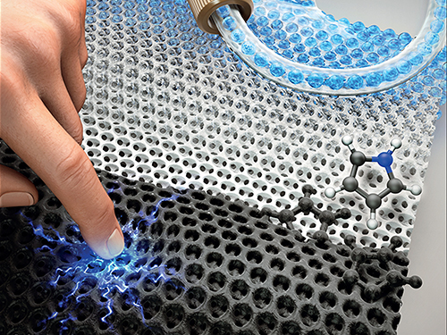
 Algorithm Identifies Optimal Pairs for Composing Metal-Organic Frameworks
The integration of metal-organic frameworks (MOFs) and other metal nanoparticles has increasingly led to the creation of new multifunctional materials. Many researchers have integrated MOFs with other classes of materials to produce new structures with synergetic properties.
Despite there being over 70,000 collections of synthesized MOFs that can be used as building blocks, the precise nature of the interaction and the bonding at the interface between the two materials still remains unknown. The question is how to sort out the right matching pairs out of 70,000 MOFs.
An algorithmic study published in Nature Communications by a KAIST research team presents a clue for finding the perfect pairs. The team, led by Professor Ji-Han Kim from the Department of Chemical and Biomolecular Engineering, developed a joint computational and experimental approach to rationally design MOF@MOFs, a composite of MOFs where an MOF is grown on a different MOF.
Professor Kim’s team, in collaboration with UNIST, noted that the metal node of one MOF can coordinately bond with the linker of a different MOF and the precisely matched interface configurations at atomic and molecular levels can enhance the likelihood of synthesizing MOF@MOFs.
They screened thousands of MOFs and identified optimal MOF pairs that can seamlessly connect to one another by taking advantage of the fact that the metal node of one MOF can form coordination bonds with the linkers of the second MOF. Six pairs predicted from the computational algorithm successfully grew into single crystals.
This computational workflow can readily extend into other classes of materials and can lead to the rapid exploration of the composite MOFs arena for accelerated materials development. Even more, the workflow can enhance the likelihood of synthesizing MOF@MOFs in the form of large single crystals, and thereby demonstrated the utility of rationally designing the MOF@MOFs.
This study is the first algorithm for predicting the synthesis of composite MOFs, to the best of their knowledge. Professor Kim said, “The number of predicted pairs can increase even more with the more general 2D lattice matching, and it is worth investigating in the future.”
This study was supported by Samsung Research Funding & Incubation Center of Samsung Electronics.
(Figure: An example of a rationally synthesized MOF@MOFs (cubic HKUST-1@MOF-5 ))
2019.08.30 View 18649
Algorithm Identifies Optimal Pairs for Composing Metal-Organic Frameworks
The integration of metal-organic frameworks (MOFs) and other metal nanoparticles has increasingly led to the creation of new multifunctional materials. Many researchers have integrated MOFs with other classes of materials to produce new structures with synergetic properties.
Despite there being over 70,000 collections of synthesized MOFs that can be used as building blocks, the precise nature of the interaction and the bonding at the interface between the two materials still remains unknown. The question is how to sort out the right matching pairs out of 70,000 MOFs.
An algorithmic study published in Nature Communications by a KAIST research team presents a clue for finding the perfect pairs. The team, led by Professor Ji-Han Kim from the Department of Chemical and Biomolecular Engineering, developed a joint computational and experimental approach to rationally design MOF@MOFs, a composite of MOFs where an MOF is grown on a different MOF.
Professor Kim’s team, in collaboration with UNIST, noted that the metal node of one MOF can coordinately bond with the linker of a different MOF and the precisely matched interface configurations at atomic and molecular levels can enhance the likelihood of synthesizing MOF@MOFs.
They screened thousands of MOFs and identified optimal MOF pairs that can seamlessly connect to one another by taking advantage of the fact that the metal node of one MOF can form coordination bonds with the linkers of the second MOF. Six pairs predicted from the computational algorithm successfully grew into single crystals.
This computational workflow can readily extend into other classes of materials and can lead to the rapid exploration of the composite MOFs arena for accelerated materials development. Even more, the workflow can enhance the likelihood of synthesizing MOF@MOFs in the form of large single crystals, and thereby demonstrated the utility of rationally designing the MOF@MOFs.
This study is the first algorithm for predicting the synthesis of composite MOFs, to the best of their knowledge. Professor Kim said, “The number of predicted pairs can increase even more with the more general 2D lattice matching, and it is worth investigating in the future.”
This study was supported by Samsung Research Funding & Incubation Center of Samsung Electronics.
(Figure: An example of a rationally synthesized MOF@MOFs (cubic HKUST-1@MOF-5 ))
2019.08.30 View 18649 -
 Highly Uniform and Low Hysteresis Pressure Sensor to Increase Practical Applicability
< Professor Steve Park (left) and the First Author Mr. Jinwon Oh (right) >
Researchers have designed a flexible pressure sensor that is expected to have a much wider applicability. A KAIST research team fabricated a piezoresistive pressure sensor of high uniformity with low hysteresis by chemically grafting a conductive polymer onto a porous elastomer template.
The team discovered that the uniformity of pore size and shape is directly related to the uniformity of the sensor. The team noted that by increasing pore size and shape variability, the variability of the sensor characteristics also increases.
Researchers led by Professor Steve Park from the Department of Materials Science and Engineering confirmed that compared to other sensors composed of randomly sized and shaped pores, which had a coefficient of variation in relative resistance change of 69.65%, their newly developed sensor exhibited much higher uniformity with a coefficient of variation of 2.43%. This study was reported in Small as the cover article on August 16.
Flexible pressure sensors have been actively researched and widely applied in electronic equipment such as touch screens, robots, wearable healthcare devices, electronic skin, and human-machine interfaces. In particular, piezoresistive pressure sensors based on elastomer‐conductive material composites hold significant potential due to their many advantages including a simple and low-cost fabrication process.
Various research results have been reported for ways to improve the performance of piezoresistive pressure sensors, most of which have been focused on increasing the sensitivity. Despite its significance, maximizing the sensitivity of composite-based piezoresistive pressure sensors is not necessary for many applications. On the other hand, sensor-to-sensor uniformity and hysteresis are two properties that are of critical importance to realize any application.
The importance of sensor-to-sensor uniformity is obvious. If the sensors manufactured under the same conditions have different properties, measurement reliability is compromised, and therefore the sensor cannot be used in a practical setting.
In addition, low hysteresis is also essential for improved measurement reliability. Hysteresis is a phenomenon in which the electrical readings differ depending on how fast or slow the sensor is being pressed, whether pressure is being released or applied, and how long and to what degree the sensor has been pressed. When a sensor has high hysteresis, the electrical readings will differ even under the same pressure, making the measurements unreliable.
Researchers said they observed a negligible hysteresis degree which was only 2%. This was attributed to the strong chemical bonding between the conductive polymer and the elastomer template, which prevents their relative sliding and displacement, and the porosity of the elastomer that enhances elastic behavior.
“This technology brings forth insight into how to address the two critical issues in pressure sensors: uniformity and hysteresis. We expect our technology to play an important role in increasing practical applications and the commercialization of pressure sensors in the near future,” said Professor Park.
This work was conducted as part of the KAIST‐funded Global Singularity Research Program for 2019, and also supported by the KUSTAR‐KAIST Institute.
Figure 1. Image of a porous elastomer template with uniform pore size and shape (left), Graph showing high uniformity in the sensors’ performance (right).
Figure 2. Hysteresis loops of the sensor at different pressure levels (left), and after a different number of cycles (right).
Figure 3. The cover page of Small Journal, Volume 15, Issue 33.
Publication:
Jinwon Oh, Jin‐Oh Kim, Yunjoo Kim, Han Byul Choi, Jun Chang Yang, Serin Lee, Mikhail Pyatykh, Jung Kim, Joo Yong Sim, and Steve Park. 2019. Highly Uniform and Low Hysteresis Piezoresistive Pressure Sensors Based on Chemical Grafting of Polypyrrole on Elastomer Template with Uniform Pore Size. Small. Wiley-VCH Verlag GmbH & Co. KgaA, Weinheim, Germany, Volume No. 15, Issue No. 33, Full Paper No. 201901744, 8 pages. https://doi.org/10.1002/smll.201901744
Profile: Prof. Steve Park, MS, PhD
stevepark@kaist.ac.kr
http://steveparklab.kaist.ac.kr/
Assistant Professor
Organic and Nano Electronics Laboratory
Department of Materials Science and Engineering
Korea Advanced Institute of Science and Technology (KAIST)
http://kaist.ac.kr
Daejeon 34141, Korea
Profile: Mr. Jinwon Oh, MS
jwoh1701@gmail.com
http://steveparklab.kaist.ac.kr/
Researcher
Organic and Nano Electronics Laboratory
Department of Materials Science and Engineering
Korea Advanced Institute of Science and Technology (KAIST)
http://kaist.ac.kr Daejeon 34141, Korea
Profile: Prof. Jung Kim, MS, PhD
jungkim@kaist.ac.kr
http://medev.kaist.ac.kr/
Professor
Biorobotics Laboratory
Department of Mechanical Engineering
Korea Advanced Institute of Science and Technology (KAIST)
http://kaist.ac.kr Daejeon 34141, Korea
Profile: Joo Yong Sim, PhD
jsim@etri.re.kr
Researcher
Bio-Medical IT Convergence Research Department
Electronics and Telecommunications Research Institute (ETRI)
https://www.etri.re.krDaejeon 34129, Korea
(END)
2019.08.19 View 30397
Highly Uniform and Low Hysteresis Pressure Sensor to Increase Practical Applicability
< Professor Steve Park (left) and the First Author Mr. Jinwon Oh (right) >
Researchers have designed a flexible pressure sensor that is expected to have a much wider applicability. A KAIST research team fabricated a piezoresistive pressure sensor of high uniformity with low hysteresis by chemically grafting a conductive polymer onto a porous elastomer template.
The team discovered that the uniformity of pore size and shape is directly related to the uniformity of the sensor. The team noted that by increasing pore size and shape variability, the variability of the sensor characteristics also increases.
Researchers led by Professor Steve Park from the Department of Materials Science and Engineering confirmed that compared to other sensors composed of randomly sized and shaped pores, which had a coefficient of variation in relative resistance change of 69.65%, their newly developed sensor exhibited much higher uniformity with a coefficient of variation of 2.43%. This study was reported in Small as the cover article on August 16.
Flexible pressure sensors have been actively researched and widely applied in electronic equipment such as touch screens, robots, wearable healthcare devices, electronic skin, and human-machine interfaces. In particular, piezoresistive pressure sensors based on elastomer‐conductive material composites hold significant potential due to their many advantages including a simple and low-cost fabrication process.
Various research results have been reported for ways to improve the performance of piezoresistive pressure sensors, most of which have been focused on increasing the sensitivity. Despite its significance, maximizing the sensitivity of composite-based piezoresistive pressure sensors is not necessary for many applications. On the other hand, sensor-to-sensor uniformity and hysteresis are two properties that are of critical importance to realize any application.
The importance of sensor-to-sensor uniformity is obvious. If the sensors manufactured under the same conditions have different properties, measurement reliability is compromised, and therefore the sensor cannot be used in a practical setting.
In addition, low hysteresis is also essential for improved measurement reliability. Hysteresis is a phenomenon in which the electrical readings differ depending on how fast or slow the sensor is being pressed, whether pressure is being released or applied, and how long and to what degree the sensor has been pressed. When a sensor has high hysteresis, the electrical readings will differ even under the same pressure, making the measurements unreliable.
Researchers said they observed a negligible hysteresis degree which was only 2%. This was attributed to the strong chemical bonding between the conductive polymer and the elastomer template, which prevents their relative sliding and displacement, and the porosity of the elastomer that enhances elastic behavior.
“This technology brings forth insight into how to address the two critical issues in pressure sensors: uniformity and hysteresis. We expect our technology to play an important role in increasing practical applications and the commercialization of pressure sensors in the near future,” said Professor Park.
This work was conducted as part of the KAIST‐funded Global Singularity Research Program for 2019, and also supported by the KUSTAR‐KAIST Institute.
Figure 1. Image of a porous elastomer template with uniform pore size and shape (left), Graph showing high uniformity in the sensors’ performance (right).
Figure 2. Hysteresis loops of the sensor at different pressure levels (left), and after a different number of cycles (right).
Figure 3. The cover page of Small Journal, Volume 15, Issue 33.
Publication:
Jinwon Oh, Jin‐Oh Kim, Yunjoo Kim, Han Byul Choi, Jun Chang Yang, Serin Lee, Mikhail Pyatykh, Jung Kim, Joo Yong Sim, and Steve Park. 2019. Highly Uniform and Low Hysteresis Piezoresistive Pressure Sensors Based on Chemical Grafting of Polypyrrole on Elastomer Template with Uniform Pore Size. Small. Wiley-VCH Verlag GmbH & Co. KgaA, Weinheim, Germany, Volume No. 15, Issue No. 33, Full Paper No. 201901744, 8 pages. https://doi.org/10.1002/smll.201901744
Profile: Prof. Steve Park, MS, PhD
stevepark@kaist.ac.kr
http://steveparklab.kaist.ac.kr/
Assistant Professor
Organic and Nano Electronics Laboratory
Department of Materials Science and Engineering
Korea Advanced Institute of Science and Technology (KAIST)
http://kaist.ac.kr
Daejeon 34141, Korea
Profile: Mr. Jinwon Oh, MS
jwoh1701@gmail.com
http://steveparklab.kaist.ac.kr/
Researcher
Organic and Nano Electronics Laboratory
Department of Materials Science and Engineering
Korea Advanced Institute of Science and Technology (KAIST)
http://kaist.ac.kr Daejeon 34141, Korea
Profile: Prof. Jung Kim, MS, PhD
jungkim@kaist.ac.kr
http://medev.kaist.ac.kr/
Professor
Biorobotics Laboratory
Department of Mechanical Engineering
Korea Advanced Institute of Science and Technology (KAIST)
http://kaist.ac.kr Daejeon 34141, Korea
Profile: Joo Yong Sim, PhD
jsim@etri.re.kr
Researcher
Bio-Medical IT Convergence Research Department
Electronics and Telecommunications Research Institute (ETRI)
https://www.etri.re.krDaejeon 34129, Korea
(END)
2019.08.19 View 30397 -
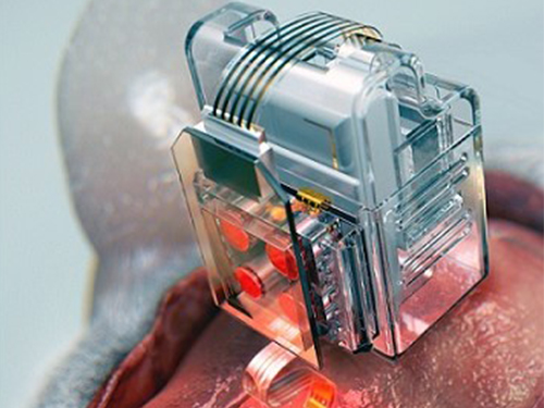 Manipulating Brain Cells by Smartphone
Researchers have developed a soft neural implant that can be wirelessly controlled using a smartphone. It is the first wireless neural device capable of indefinitely delivering multiple drugs and multiple colour lights, which neuroscientists believe can speed up efforts to uncover brain diseases such as Parkinson’s, Alzheimer’s, addiction, depression, and pain.
A team under Professor Jae-Woong Jeong from the School of Electrical Engineering at KAIST and his collaborators have invented a device that can control neural circuits using a tiny brain implant controlled by a smartphone. The device, using Lego-like replaceable drug cartridges and powerful, low-energy Bluetooth, can target specific neurons of interest using drugs and light for prolonged periods. This study was published in Nature Biomedical Engineering.
“This novel device is the fruit of advanced electronics design and powerful micro and nanoscale engineering,” explained Professor Jeong. “We are interested in further developing this technology to make a brain implant for clinical applications.”
This technology significantly overshadows the conventional methods used by neuroscientists, which usually involve rigid metal tubes and optical fibers to deliver drugs and light. Apart from limiting the subject’s movement due to bulky equipment, their relatively rigid structure causes lesions in soft brain tissue over time, therefore making them not suitable for long-term implantation. Although some efforts have been made to partly mitigate adverse tissue response by incorporating soft probes and wireless platforms, the previous solutions were limited by their inability to deliver drugs for long periods of time as well as their bulky and complex control setups.
To achieve chronic wireless drug delivery, scientists had to solve the critical challenge of the exhaustion and evaporation of drugs. To combat this, the researchers invented a neural device with a replaceable drug cartridge, which could allow neuroscientists to study the same brain circuits for several months without worrying about running out of drugs.
These ‘plug-n-play’ drug cartridges were assembled into a brain implant for mice with a soft and ultrathin probe (with the thickness of a human hair), which consisted of microfluidic channels and tiny LEDs (smaller than a grain of salt), for unlimited drug doses and light delivery.
Controlled with an elegant and simple user interface on a smartphone, neuroscientists can easily trigger any specific combination or precise sequencing of light and drug delivery in any implanted target animal without the need to be physically inside the laboratory. Using these wireless neural devices, researchers can also easily setup fully automated animal studies where the behaviour of one animal could affect other animals by triggering light and/or drug delivery.
“The wireless neural device enables chronic chemical and optical neuromodulation that has never been achieved before,” said lead author Raza Qazi, a researcher with KAIST and the University of Colorado Boulder.
This work was supported by grants from the National Research Foundation of Korea, US National Institute of Health, National Institute on Drug Abuse, and Mallinckrodt Professorship.
(A neural implant with replaceable drug cartridges and Bluetooth low-energy can target specific neurons .)
(Micro LED controlling using smartphone application)
2019.08.07 View 34981
Manipulating Brain Cells by Smartphone
Researchers have developed a soft neural implant that can be wirelessly controlled using a smartphone. It is the first wireless neural device capable of indefinitely delivering multiple drugs and multiple colour lights, which neuroscientists believe can speed up efforts to uncover brain diseases such as Parkinson’s, Alzheimer’s, addiction, depression, and pain.
A team under Professor Jae-Woong Jeong from the School of Electrical Engineering at KAIST and his collaborators have invented a device that can control neural circuits using a tiny brain implant controlled by a smartphone. The device, using Lego-like replaceable drug cartridges and powerful, low-energy Bluetooth, can target specific neurons of interest using drugs and light for prolonged periods. This study was published in Nature Biomedical Engineering.
“This novel device is the fruit of advanced electronics design and powerful micro and nanoscale engineering,” explained Professor Jeong. “We are interested in further developing this technology to make a brain implant for clinical applications.”
This technology significantly overshadows the conventional methods used by neuroscientists, which usually involve rigid metal tubes and optical fibers to deliver drugs and light. Apart from limiting the subject’s movement due to bulky equipment, their relatively rigid structure causes lesions in soft brain tissue over time, therefore making them not suitable for long-term implantation. Although some efforts have been made to partly mitigate adverse tissue response by incorporating soft probes and wireless platforms, the previous solutions were limited by their inability to deliver drugs for long periods of time as well as their bulky and complex control setups.
To achieve chronic wireless drug delivery, scientists had to solve the critical challenge of the exhaustion and evaporation of drugs. To combat this, the researchers invented a neural device with a replaceable drug cartridge, which could allow neuroscientists to study the same brain circuits for several months without worrying about running out of drugs.
These ‘plug-n-play’ drug cartridges were assembled into a brain implant for mice with a soft and ultrathin probe (with the thickness of a human hair), which consisted of microfluidic channels and tiny LEDs (smaller than a grain of salt), for unlimited drug doses and light delivery.
Controlled with an elegant and simple user interface on a smartphone, neuroscientists can easily trigger any specific combination or precise sequencing of light and drug delivery in any implanted target animal without the need to be physically inside the laboratory. Using these wireless neural devices, researchers can also easily setup fully automated animal studies where the behaviour of one animal could affect other animals by triggering light and/or drug delivery.
“The wireless neural device enables chronic chemical and optical neuromodulation that has never been achieved before,” said lead author Raza Qazi, a researcher with KAIST and the University of Colorado Boulder.
This work was supported by grants from the National Research Foundation of Korea, US National Institute of Health, National Institute on Drug Abuse, and Mallinckrodt Professorship.
(A neural implant with replaceable drug cartridges and Bluetooth low-energy can target specific neurons .)
(Micro LED controlling using smartphone application)
2019.08.07 View 34981 -
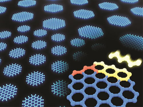 Synthesizing Single-Crystalline Hexagonal Graphene Quantum Dots
(Figure: Uniformly ordered single-crystalline graphene quantum dots of various sizes synthesized through solution chemistry.)
A KAIST team has designed a novel strategy for synthesizing single-crystalline graphene quantum dots, which emit stable blue light. The research team confirmed that a display made of their synthesized graphene quantum dots successfully emitted blue light with stable electric pressure, reportedly resolving the long-standing challenges of blue light emission in manufactured displays. The study, led by Professor O Ok Park in the Department of Chemical and Biological Engineering, was featured online in Nano Letters on July 5.
Graphene has gained increased attention as a next-generation material for its heat and electrical conductivity as well as its transparency. However, single and multi-layered graphene have characteristics of a conductor so that it is difficult to apply into semiconductor. Only when downsized to the nanoscale, semiconductor’s distinct feature of bandgap will be exhibited to emit the light in the graphene. This illuminating featuring of dot is referred to as a graphene quantum dot.
Conventionally, single-crystalline graphene has been fabricated by chemical vapor deposition (CVD) on copper or nickel thin films, or by peeling graphite physically and chemically. However, graphene made via chemical vapor deposition is mainly used for large-surface transparent electrodes. Meanwhile, graphene made by chemical and physical peeling carries uneven size defects.
The research team explained that their graphene quantum dots exhibited a very stable single-phase reaction when they mixed amine and acetic acid with an aqueous solution of glucose. Then, they synthesized single-crystalline graphene quantum dots from the self-assembly of the reaction intermediate. In the course of fabrication, the team developed a new separation method at a low-temperature precipitation, which led to successfully creating a homogeneous nucleation of graphene quantum dots via a single-phase reaction.
Professor Park and his colleagues have developed solution phase synthesis technology that allows for the creation of the desired crystal size for single nanocrystals down to 100 nano meters. It is reportedly the first synthesis of the homogeneous nucleation of graphene through a single-phase reaction.
Professor Park said, "This solution method will significantly contribute to the grafting of graphene in various fields. The application of this new graphene will expand the scope of its applications such as for flexible displays and varistors.”
This research was a joint project with a team from Korea University under Professor Sang Hyuk Im from the Department of Chemical and Biological Engineering, and was supported by the National Research Foundation of Korea, the Nano-Material Technology Development Program from the Electronics and Telecommunications Research Institute (ETRI), KAIST EEWS, and the BK21+ project from the Korean government.
2019.08.02 View 36487
Synthesizing Single-Crystalline Hexagonal Graphene Quantum Dots
(Figure: Uniformly ordered single-crystalline graphene quantum dots of various sizes synthesized through solution chemistry.)
A KAIST team has designed a novel strategy for synthesizing single-crystalline graphene quantum dots, which emit stable blue light. The research team confirmed that a display made of their synthesized graphene quantum dots successfully emitted blue light with stable electric pressure, reportedly resolving the long-standing challenges of blue light emission in manufactured displays. The study, led by Professor O Ok Park in the Department of Chemical and Biological Engineering, was featured online in Nano Letters on July 5.
Graphene has gained increased attention as a next-generation material for its heat and electrical conductivity as well as its transparency. However, single and multi-layered graphene have characteristics of a conductor so that it is difficult to apply into semiconductor. Only when downsized to the nanoscale, semiconductor’s distinct feature of bandgap will be exhibited to emit the light in the graphene. This illuminating featuring of dot is referred to as a graphene quantum dot.
Conventionally, single-crystalline graphene has been fabricated by chemical vapor deposition (CVD) on copper or nickel thin films, or by peeling graphite physically and chemically. However, graphene made via chemical vapor deposition is mainly used for large-surface transparent electrodes. Meanwhile, graphene made by chemical and physical peeling carries uneven size defects.
The research team explained that their graphene quantum dots exhibited a very stable single-phase reaction when they mixed amine and acetic acid with an aqueous solution of glucose. Then, they synthesized single-crystalline graphene quantum dots from the self-assembly of the reaction intermediate. In the course of fabrication, the team developed a new separation method at a low-temperature precipitation, which led to successfully creating a homogeneous nucleation of graphene quantum dots via a single-phase reaction.
Professor Park and his colleagues have developed solution phase synthesis technology that allows for the creation of the desired crystal size for single nanocrystals down to 100 nano meters. It is reportedly the first synthesis of the homogeneous nucleation of graphene through a single-phase reaction.
Professor Park said, "This solution method will significantly contribute to the grafting of graphene in various fields. The application of this new graphene will expand the scope of its applications such as for flexible displays and varistors.”
This research was a joint project with a team from Korea University under Professor Sang Hyuk Im from the Department of Chemical and Biological Engineering, and was supported by the National Research Foundation of Korea, the Nano-Material Technology Development Program from the Electronics and Telecommunications Research Institute (ETRI), KAIST EEWS, and the BK21+ project from the Korean government.
2019.08.02 View 36487