device
-
 KAIST Develops a Credit-Card-Thick Flexible Lithium Ion Battery
Since the battery can be charged wirelessly, useful applications are expected including medical patches and smart cards.
Professor Jang Wook Choi at KAIST’s Graduate School of Energy, Environment, Water, and Sustainability (EEWS) and Dr. Jae Yong Song at the Korea Research Institute of Standards and Science jointly led research to invent a flexible lithium ion battery that is thinner than a credit card and can be charged wirelessly.
Their research findings were published online in Nano Letters on March 6, 2015. Lithium ion batteries are widely used today in various electronics including mobile devices and electronic cars. Researchers said that their work could help accelerate the development of flexible and wearable electronics.
Conventional lithium ion batteries are manufactured based on a layering technology, stacking up anodes, separating films, and cathodes like a sandwich, which makes it difficult to reduce their thickness. In addition, friction arises between layers, making the batteries impossible to bend. The coating films of electrodes easily come off, which contributes to the batteries’ poor performance.
The research team abandoned the existing production technology. Instead, they removed the separating films, layered the cathodes and anodes collinearly on a plane, and created a partition between electrodes to eliminate potential problems, such as short circuits and voltage dips, commonly present in lithium ion batteries.
After more than five thousand consecutive flexing experiments, the research team confirmed the possibility of a more flexible electrode structure while maintaining the battery performance comparable to the level of current lithium ion batteries.
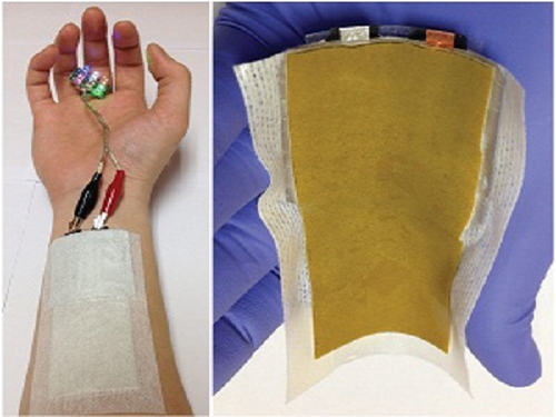
Flexible batteries can be applied to integrated smart cards, cosmetic and medical patches, and skin adhesive sensors that can control a computer with voice commands or gesture as seen in the movie “Iron Man.”
Moreover, the team has successfully developed wireless-charging technology using electromagnetic induction and solar batteries.
They are currently developing a mass production process to combine this planar battery technology and printing, to ultimately create a new paradigm to print semiconductors and batteries using 3D printers.
Professor Choi said, “This new technology will contribute to diversifying patch functions as it is applicable to power various adhesive medical patches.”
Picture 1: Medical patch (left) and flexible secondary battery (right)
Picture 2: Diagram of flexible battery
Picture 3: Smart card embedding flexible battery
2015.03.24 View 12989
KAIST Develops a Credit-Card-Thick Flexible Lithium Ion Battery
Since the battery can be charged wirelessly, useful applications are expected including medical patches and smart cards.
Professor Jang Wook Choi at KAIST’s Graduate School of Energy, Environment, Water, and Sustainability (EEWS) and Dr. Jae Yong Song at the Korea Research Institute of Standards and Science jointly led research to invent a flexible lithium ion battery that is thinner than a credit card and can be charged wirelessly.
Their research findings were published online in Nano Letters on March 6, 2015. Lithium ion batteries are widely used today in various electronics including mobile devices and electronic cars. Researchers said that their work could help accelerate the development of flexible and wearable electronics.
Conventional lithium ion batteries are manufactured based on a layering technology, stacking up anodes, separating films, and cathodes like a sandwich, which makes it difficult to reduce their thickness. In addition, friction arises between layers, making the batteries impossible to bend. The coating films of electrodes easily come off, which contributes to the batteries’ poor performance.
The research team abandoned the existing production technology. Instead, they removed the separating films, layered the cathodes and anodes collinearly on a plane, and created a partition between electrodes to eliminate potential problems, such as short circuits and voltage dips, commonly present in lithium ion batteries.
After more than five thousand consecutive flexing experiments, the research team confirmed the possibility of a more flexible electrode structure while maintaining the battery performance comparable to the level of current lithium ion batteries.
Flexible batteries can be applied to integrated smart cards, cosmetic and medical patches, and skin adhesive sensors that can control a computer with voice commands or gesture as seen in the movie “Iron Man.”
Moreover, the team has successfully developed wireless-charging technology using electromagnetic induction and solar batteries.
They are currently developing a mass production process to combine this planar battery technology and printing, to ultimately create a new paradigm to print semiconductors and batteries using 3D printers.
Professor Choi said, “This new technology will contribute to diversifying patch functions as it is applicable to power various adhesive medical patches.”
Picture 1: Medical patch (left) and flexible secondary battery (right)
Picture 2: Diagram of flexible battery
Picture 3: Smart card embedding flexible battery
2015.03.24 View 12989 -
 KAIST Develops Subminiature, Power-Efficient Air Pollution Sensing Probe
Professor Inkyu Park and his research team from the Department of Mechanical Engineering at KAIST have developed a subminiature, power-efficient air-pollution sensing probe that can be applied to mobile devices. Their research findings were published online in the January 30th issue of Scientific Reports.
As air pollution has increased, people have taken greater interest in health care. The developed technology could allow people to measure independently the air pollution level of their surrounding environments.
Previous instruments used to measure air pollution levels were bulky and consumed a lot of power. They also often produced inaccurate results when measuring air pollution in which different toxic gases were mixed. These problems could not be resolved with existing semiconductor manufacturing process.
Using local temperature field control technology, Professor Park’s team succeeded in integrating multiple heterogeneous nanomaterials and fitting them onto a small, low-power electronic chip. This microheating sensor can heat microscale regions through local hydrothermal synthesis. Because it requires a miniscale amount of nanomaterials to manufacture, the sensor is most suitable for mobile devices.
Professor Park said, “Our research will contribute to the development of convergence technology in such field as air pollution sensing probes, biosensors, electronic devices, and displays.”
The team's research was supported by the Ministry of Education and the Ministry of Science, ICT and Future Planning, Republic of Korea.
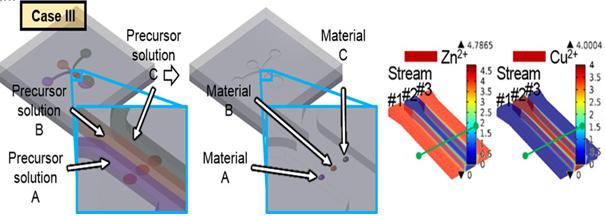
Figure 1 – The Concept of Multiple Nanomaterial Device and Numerical Simulation Results of Precursor Solutions
Figure 2 - Multiple Nanomaterial Manufactured in a Microscale Region
2015.02.27 View 11282
KAIST Develops Subminiature, Power-Efficient Air Pollution Sensing Probe
Professor Inkyu Park and his research team from the Department of Mechanical Engineering at KAIST have developed a subminiature, power-efficient air-pollution sensing probe that can be applied to mobile devices. Their research findings were published online in the January 30th issue of Scientific Reports.
As air pollution has increased, people have taken greater interest in health care. The developed technology could allow people to measure independently the air pollution level of their surrounding environments.
Previous instruments used to measure air pollution levels were bulky and consumed a lot of power. They also often produced inaccurate results when measuring air pollution in which different toxic gases were mixed. These problems could not be resolved with existing semiconductor manufacturing process.
Using local temperature field control technology, Professor Park’s team succeeded in integrating multiple heterogeneous nanomaterials and fitting them onto a small, low-power electronic chip. This microheating sensor can heat microscale regions through local hydrothermal synthesis. Because it requires a miniscale amount of nanomaterials to manufacture, the sensor is most suitable for mobile devices.
Professor Park said, “Our research will contribute to the development of convergence technology in such field as air pollution sensing probes, biosensors, electronic devices, and displays.”
The team's research was supported by the Ministry of Education and the Ministry of Science, ICT and Future Planning, Republic of Korea.
Figure 1 – The Concept of Multiple Nanomaterial Device and Numerical Simulation Results of Precursor Solutions
Figure 2 - Multiple Nanomaterial Manufactured in a Microscale Region
2015.02.27 View 11282 -
 KAIST's Thermoelectric Generator on Glass Fabric Receives the Grand Prize at the Netexplo Forum 2015
The forum announced top ten IT innovations expected to change the world and selected the grand prize on February 4, 2014.
Established in 2007 by Martine Bidegain and Thierry Happe in partnership with the French Senate and the French Ministry for the Digital Economy, the Netexplo Observatory is an independent global organization that studies the impact of digital technology and innovation on society and business.
Every year, the Netexplo Observatory hosts an international conference, the Netexplo Forum, in Paris, France, which surveys digital innovation worldwide. The 8th forum was held in partnership with the United Nations Educational, Scientific and Cultural Organization (UNESCO) on February 4-5, 2015, at the UNESCO House in Paris.
Prior to the conference, the Netexplo Forum 2015 named the top ten most promising digital technologies that will greatly impact the world.
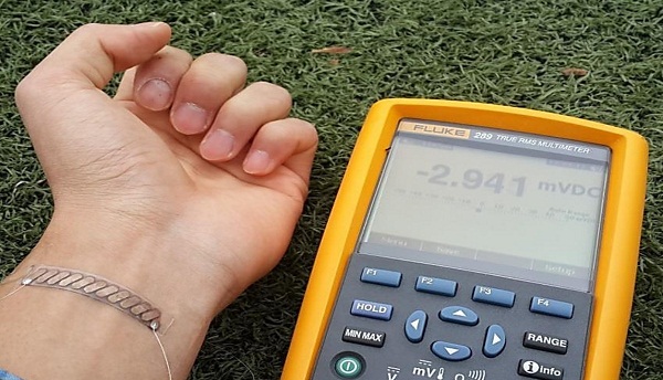
Among them was Professor Byung Jin Cho’s research on a wearable thermoelectric generator (http://www.eurekalert.org/pub_releases/2014-04/tkai-tgo041014.php). The generator was selected as the most innovative technology this year.
Professor Cho of KAIST’s Electrical Engineering Department developed a glass fabric-based thermoelectric generator that is extremely light and flexible and that produces electricity from the heat of the human body. This technology can be applied widely to wearable computers and mobile devices.
The full list of innovations follows below:
Wearable Thermo-Element, South Korea: The human body becomes a source of energy for mobile devices.
W.Afate 3D-printer, Togo: An environmentally friendly fablab that makes a low-cost 3D-printer from recycling electronic components.
Slack, USA: By combining email, Skype, and file-sharing and social networks, internal communication becomes much easier and simpler.
PhotoMath, Croatia: A free app that enables smartphone users to solve mathematical problems simply by scanning the mathematical texts.
Kappo, Chile: Connected cyclists produce and transmit useful data for urban planning to make the city more bike-friendly.
Branching Minds, USA: An improved learning process for students in difficulty through a personalized approach.
Baidu Kuai Sou, China: Smart chopsticks that can check food hazards.
SCio, Israel: A pocket molecular sensor with various applications and data
Rainforest Connection, USA: Fighting deforestation with recycled smartphones
Sense Ebola Followup, Nigeria: A mobile tool to help contain Ebola
For more details on the wearable thermos-element which received the 2015 Netexplo Award, please go to https://www.netexplo.org/en/intelligence/innovation/wearable-thermo-element.
Pictures 1 and 2: A high-performance wearable thermoelectric generator that is extremely flexible and light.
Picture 3: Senator Catherine Morin-Desailly (left) of the French Parliament presents the 2015 Netexplo Award to Professor Byung Jin Cho (right) on February 4, 2015 at the UNESCO House in Paris.
Credit of Loran Dhérines
Picture 4: Professor Byung Jin Cho (left) poses with Dr. Joël de Rosnay (right).
Credit of Loran Dhérines
2015.02.06 View 14969
KAIST's Thermoelectric Generator on Glass Fabric Receives the Grand Prize at the Netexplo Forum 2015
The forum announced top ten IT innovations expected to change the world and selected the grand prize on February 4, 2014.
Established in 2007 by Martine Bidegain and Thierry Happe in partnership with the French Senate and the French Ministry for the Digital Economy, the Netexplo Observatory is an independent global organization that studies the impact of digital technology and innovation on society and business.
Every year, the Netexplo Observatory hosts an international conference, the Netexplo Forum, in Paris, France, which surveys digital innovation worldwide. The 8th forum was held in partnership with the United Nations Educational, Scientific and Cultural Organization (UNESCO) on February 4-5, 2015, at the UNESCO House in Paris.
Prior to the conference, the Netexplo Forum 2015 named the top ten most promising digital technologies that will greatly impact the world.
Among them was Professor Byung Jin Cho’s research on a wearable thermoelectric generator (http://www.eurekalert.org/pub_releases/2014-04/tkai-tgo041014.php). The generator was selected as the most innovative technology this year.
Professor Cho of KAIST’s Electrical Engineering Department developed a glass fabric-based thermoelectric generator that is extremely light and flexible and that produces electricity from the heat of the human body. This technology can be applied widely to wearable computers and mobile devices.
The full list of innovations follows below:
Wearable Thermo-Element, South Korea: The human body becomes a source of energy for mobile devices.
W.Afate 3D-printer, Togo: An environmentally friendly fablab that makes a low-cost 3D-printer from recycling electronic components.
Slack, USA: By combining email, Skype, and file-sharing and social networks, internal communication becomes much easier and simpler.
PhotoMath, Croatia: A free app that enables smartphone users to solve mathematical problems simply by scanning the mathematical texts.
Kappo, Chile: Connected cyclists produce and transmit useful data for urban planning to make the city more bike-friendly.
Branching Minds, USA: An improved learning process for students in difficulty through a personalized approach.
Baidu Kuai Sou, China: Smart chopsticks that can check food hazards.
SCio, Israel: A pocket molecular sensor with various applications and data
Rainforest Connection, USA: Fighting deforestation with recycled smartphones
Sense Ebola Followup, Nigeria: A mobile tool to help contain Ebola
For more details on the wearable thermos-element which received the 2015 Netexplo Award, please go to https://www.netexplo.org/en/intelligence/innovation/wearable-thermo-element.
Pictures 1 and 2: A high-performance wearable thermoelectric generator that is extremely flexible and light.
Picture 3: Senator Catherine Morin-Desailly (left) of the French Parliament presents the 2015 Netexplo Award to Professor Byung Jin Cho (right) on February 4, 2015 at the UNESCO House in Paris.
Credit of Loran Dhérines
Picture 4: Professor Byung Jin Cho (left) poses with Dr. Joël de Rosnay (right).
Credit of Loran Dhérines
2015.02.06 View 14969 -
 Press Release on Piezoelectric Nanogenerators of ZnO with Aluminium Nitride Stacked Layers by the American Institute of Physics
The
American Institute of Physics (AIP) released a news article entitled “Zinc
Oxide Materials Tapped for Tiny Energy Harvesting Devices” on January 13, 2015.
The
article described the research led by Professor Giwan Yoon of the
Electrical Engineering Department at KAIST. It was published in the January
12, 2015 issue of Applied Physics Letters.
AIP publishes the journal. For the news release, please visit the
link below:
The American
Institute of Physics, January 13, 2015
“Zinc
Oxide Materials Tapped for Tiny Energy Harvesting Devices”
New research helps
pave the way toward highly energy-efficient zinc oxide-based micro energy
harvesting devices with applications in portable communications, healthcare and
environmental monitoring, and more
http://www.aip.org/publishing/journal-highlights/zinc-oxide-materials-tapped-tiny-energy-harvesting-devices
2015.02.04 View 33477
Press Release on Piezoelectric Nanogenerators of ZnO with Aluminium Nitride Stacked Layers by the American Institute of Physics
The
American Institute of Physics (AIP) released a news article entitled “Zinc
Oxide Materials Tapped for Tiny Energy Harvesting Devices” on January 13, 2015.
The
article described the research led by Professor Giwan Yoon of the
Electrical Engineering Department at KAIST. It was published in the January
12, 2015 issue of Applied Physics Letters.
AIP publishes the journal. For the news release, please visit the
link below:
The American
Institute of Physics, January 13, 2015
“Zinc
Oxide Materials Tapped for Tiny Energy Harvesting Devices”
New research helps
pave the way toward highly energy-efficient zinc oxide-based micro energy
harvesting devices with applications in portable communications, healthcare and
environmental monitoring, and more
http://www.aip.org/publishing/journal-highlights/zinc-oxide-materials-tapped-tiny-energy-harvesting-devices
2015.02.04 View 33477 -
 KAIST Develops a Method to Transfer Graphene by Stamping
Professor Sung-Yool Choi’s research team from KAIST's Department of Electrical Engineering has developed a technique that can produce a single-layer graphene from a metal etching. Through this, transferring a graphene layer onto a circuit board can be done as easily as stamping a seal on paper.
The research findings were published in the January 14th issue of Small as the lead article.
This technology will allow different types of wafer transfer methods such as transfer onto a surface of a device or a curved surface, and large surface transfer onto a 4 inch wafer. It will be applied in the field of wearable smart gadgets through commercialization of graphene electronic devices.
The traditional method used to transfer graphene onto a circuit board is a wet transfer. However, it has some drawbacks as the graphene layer can be damaged or contaminated during the transfer process from residue from the metal etching. This may affect the electrical properties of the transferred graphene.
After a graphene growth substrate formed on a catalytic metal substrate is pretreated in an aqueous poly vinyl alcohol (PVA) solution, a PVA film forms on the pretreated substrate. The substrate and the graphene layers bond strongly. The graphene is lifted from the growth substrate by means of an elastomeric stamp.
The delaminated graphene layer is isolated state from the elastomeric stamp and thus can be freely transferred onto a circuit board. As the catalytic metal substrate can be reused and does not contain harmful chemical substances, such transfer method is very eco-friendly.
Professor Choi said, “As the new graphene transfer method has a wide range of applications and allows a large surface transfer, it will contribute to the commercialization of graphene electronic devices.” He added that “because this technique has a high degree of freedom in transfer process, it has a variety of usages for graphene and 2 dimensional nano-devices.”
This research was sponsored by the Ministry of Science, ICT and Future Planning, the Republic of Korea.
Figure 1. Cover photo of the journal Small which illustrates the research findings
Figure 2. Above view of Graphene layer transferred through the new method
Figure 3. Large surface transfer of Graphene
2015.01.23 View 11748
KAIST Develops a Method to Transfer Graphene by Stamping
Professor Sung-Yool Choi’s research team from KAIST's Department of Electrical Engineering has developed a technique that can produce a single-layer graphene from a metal etching. Through this, transferring a graphene layer onto a circuit board can be done as easily as stamping a seal on paper.
The research findings were published in the January 14th issue of Small as the lead article.
This technology will allow different types of wafer transfer methods such as transfer onto a surface of a device or a curved surface, and large surface transfer onto a 4 inch wafer. It will be applied in the field of wearable smart gadgets through commercialization of graphene electronic devices.
The traditional method used to transfer graphene onto a circuit board is a wet transfer. However, it has some drawbacks as the graphene layer can be damaged or contaminated during the transfer process from residue from the metal etching. This may affect the electrical properties of the transferred graphene.
After a graphene growth substrate formed on a catalytic metal substrate is pretreated in an aqueous poly vinyl alcohol (PVA) solution, a PVA film forms on the pretreated substrate. The substrate and the graphene layers bond strongly. The graphene is lifted from the growth substrate by means of an elastomeric stamp.
The delaminated graphene layer is isolated state from the elastomeric stamp and thus can be freely transferred onto a circuit board. As the catalytic metal substrate can be reused and does not contain harmful chemical substances, such transfer method is very eco-friendly.
Professor Choi said, “As the new graphene transfer method has a wide range of applications and allows a large surface transfer, it will contribute to the commercialization of graphene electronic devices.” He added that “because this technique has a high degree of freedom in transfer process, it has a variety of usages for graphene and 2 dimensional nano-devices.”
This research was sponsored by the Ministry of Science, ICT and Future Planning, the Republic of Korea.
Figure 1. Cover photo of the journal Small which illustrates the research findings
Figure 2. Above view of Graphene layer transferred through the new method
Figure 3. Large surface transfer of Graphene
2015.01.23 View 11748 -
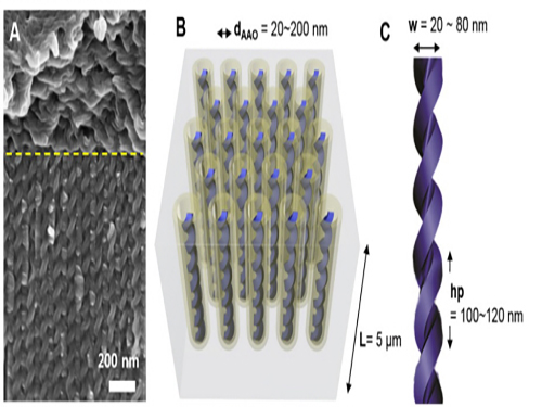 KAIST Develops Core Technology to Synthesize a Helical Nanostructure
Professor Dong-Ki Yoon’s research team of the Graduate School of Nanoscience and Technology (GSNT) at KAIST has developed helical nanostructures using self-assembly processes. The results were published in the Proceedings of the National Academy of Sciences of the United States of America(PNAS) on the October 7th.
This technology enables the synthesis of various helical structures on a relatively large confined area. Its synthesis is often considered the most arduous for three dimensional structures. Formed from liquid crystal, the structure holds a regular helical structure within the confined space of 20 to 300 nanometers. Also, the distance between each pattern increased as the diameter of the nanostructure increased.
Liquid crystals have a unique property of responding sensitively to the surrounding electromagnetic field. The technology, in combination with the electromagnetic property of liquid crystal, is expected to foster the development of highly efficient optoelectronic devices.
Using this technology, it is possible to develop three dimensional patterning technology beyond the current semiconductor manufacturing technology which uses two dimensional photolithography processes. Three-dimensional semiconductor devices are expected to store hundred times more data than current devices. They will also lower costs by simplifying manufacturing processes.
The essence of this research, “self-assembly in confined space,” refers to controlling complex nanostructures, which can be synthesized from materials such as macromolecules, liquid crystal molecules, and biomolecules in relation to surrounding environments including the temperature, concentration, and pH.
The research team produced a confined space with a length of tens of nanometers by using a porous anodized aluminum membrane induced from an electrochemical reaction. They successfully synthesized independently controlled helical nanostructures by forming the helical structures from liquid crystal molecules within that space.
Professor Yoon said, “This research examines the physicochemical principle of controlling helical nanostructures.” He highlighted the significance of the research and commented, “The technology enables the control of complex nanostructures from organic molecules by using confined space and surface reforming.”
He added that, “When grafted with nanotechnology or information technology, this technology will spur new growth to liquid crystal-related industries such as the LCD.”
The research was led by two Ph.D. candidates, Hanim Kim and Sunhee Lee, under the guidance of Professor Yoon. Dr. Tae-Joo Shin of the Pohang Accelerator Laboratory, Professor Sang-Bok Lee of the University of Maryland, and Professor Noel Clark of the University of Colorado also participated.
Picture 1. Electron Microscopy Pictures and Conceptual Diagrams of Helical Nanostructures
Picture 2. Electron Microscopy Pictures of Manufactured Helical Nanostructures
2014.10.29 View 9418
KAIST Develops Core Technology to Synthesize a Helical Nanostructure
Professor Dong-Ki Yoon’s research team of the Graduate School of Nanoscience and Technology (GSNT) at KAIST has developed helical nanostructures using self-assembly processes. The results were published in the Proceedings of the National Academy of Sciences of the United States of America(PNAS) on the October 7th.
This technology enables the synthesis of various helical structures on a relatively large confined area. Its synthesis is often considered the most arduous for three dimensional structures. Formed from liquid crystal, the structure holds a regular helical structure within the confined space of 20 to 300 nanometers. Also, the distance between each pattern increased as the diameter of the nanostructure increased.
Liquid crystals have a unique property of responding sensitively to the surrounding electromagnetic field. The technology, in combination with the electromagnetic property of liquid crystal, is expected to foster the development of highly efficient optoelectronic devices.
Using this technology, it is possible to develop three dimensional patterning technology beyond the current semiconductor manufacturing technology which uses two dimensional photolithography processes. Three-dimensional semiconductor devices are expected to store hundred times more data than current devices. They will also lower costs by simplifying manufacturing processes.
The essence of this research, “self-assembly in confined space,” refers to controlling complex nanostructures, which can be synthesized from materials such as macromolecules, liquid crystal molecules, and biomolecules in relation to surrounding environments including the temperature, concentration, and pH.
The research team produced a confined space with a length of tens of nanometers by using a porous anodized aluminum membrane induced from an electrochemical reaction. They successfully synthesized independently controlled helical nanostructures by forming the helical structures from liquid crystal molecules within that space.
Professor Yoon said, “This research examines the physicochemical principle of controlling helical nanostructures.” He highlighted the significance of the research and commented, “The technology enables the control of complex nanostructures from organic molecules by using confined space and surface reforming.”
He added that, “When grafted with nanotechnology or information technology, this technology will spur new growth to liquid crystal-related industries such as the LCD.”
The research was led by two Ph.D. candidates, Hanim Kim and Sunhee Lee, under the guidance of Professor Yoon. Dr. Tae-Joo Shin of the Pohang Accelerator Laboratory, Professor Sang-Bok Lee of the University of Maryland, and Professor Noel Clark of the University of Colorado also participated.
Picture 1. Electron Microscopy Pictures and Conceptual Diagrams of Helical Nanostructures
Picture 2. Electron Microscopy Pictures of Manufactured Helical Nanostructures
2014.10.29 View 9418 -
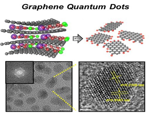 Extracting Light from Graphite: Core Technology of Graphene Quantum Dots Display Developed
Professor Seokwoo Jeon of the Department of Materials Science and Engineering, Professor Yong-Hoon Cho of the Department of Physics, and Professor Seunghyup Yoo of the Department of Electrical Engineering announced that they were able to develop topnotch graphene quantum dots from graphite.
Using the method of synthesizing graphite intercalation compound from graphite with salt and water, the research team developed graphene quantum dots in an ecofriendly way.
The quantum dots have a diameter of 5 nanometers with their sizes equal and yield high quantum efficiency. Unlike conventional quantum dots, they are not comprised of toxic materials such as lead or cadmium. As the quantum dots can be developed from materials which can be easily found in the nature, researchers look forward to putting these into mass production at low cost.
The research team also discovered a luminescence mechanism of graphene quantum dots and confirmed the possibility of commercial use by developing quantum dot light-emitting diodes with brightness of 1,000 cd/m2, which is greater than that of cellphone displays.
Professor Seokwoo Jeon said, “Although quantum dot LEDs have a lower luminous efficiency than existing ones, their luminescent property can be further improved” and emphasized that “using quantum dot displays will allow us to develop not only paper-thin displays but also flexible ones.”
Sponsored by Graphene Research Center in KAIST Institute for NanoCentury, the research finding was published online in the April 20th issue of Advanced Optical Materials.
Picture 1: Graphene quantum dots and their synthesis
Picture 2: Luminescence mechanism of graphene quantum dots
Picture 3: Structure of graphene quantum dots LED and its emission
2014.09.06 View 18625
Extracting Light from Graphite: Core Technology of Graphene Quantum Dots Display Developed
Professor Seokwoo Jeon of the Department of Materials Science and Engineering, Professor Yong-Hoon Cho of the Department of Physics, and Professor Seunghyup Yoo of the Department of Electrical Engineering announced that they were able to develop topnotch graphene quantum dots from graphite.
Using the method of synthesizing graphite intercalation compound from graphite with salt and water, the research team developed graphene quantum dots in an ecofriendly way.
The quantum dots have a diameter of 5 nanometers with their sizes equal and yield high quantum efficiency. Unlike conventional quantum dots, they are not comprised of toxic materials such as lead or cadmium. As the quantum dots can be developed from materials which can be easily found in the nature, researchers look forward to putting these into mass production at low cost.
The research team also discovered a luminescence mechanism of graphene quantum dots and confirmed the possibility of commercial use by developing quantum dot light-emitting diodes with brightness of 1,000 cd/m2, which is greater than that of cellphone displays.
Professor Seokwoo Jeon said, “Although quantum dot LEDs have a lower luminous efficiency than existing ones, their luminescent property can be further improved” and emphasized that “using quantum dot displays will allow us to develop not only paper-thin displays but also flexible ones.”
Sponsored by Graphene Research Center in KAIST Institute for NanoCentury, the research finding was published online in the April 20th issue of Advanced Optical Materials.
Picture 1: Graphene quantum dots and their synthesis
Picture 2: Luminescence mechanism of graphene quantum dots
Picture 3: Structure of graphene quantum dots LED and its emission
2014.09.06 View 18625 -
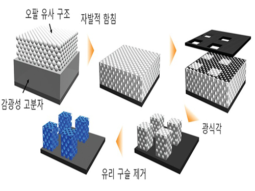 Clear Display Technology Under Sunlight Developed
The late Professor Seung-Man Yang
The last paper of the late Professor Seung-Man Yang, who was a past master of colloids and fluid mechanics
Practical patterning technology of the next generation optical materials, photonic crystals
The mineral opal does not possess any pigments, but it appears colorful to our eyes. This is because only a particular wavelength is reflected due to the regular nano-structure of its surface. The material that causes selective reflection of the light is called photonic crystals.
The deceased Professor Seung-Man Yang and his research team from KAIST’s Chemical and Biomolecular Engineering Department ha ve developed micro-pattern technology using photolithographic process. This can accelerate the commercialization of photonic crystals, which is hailed as the next generation optics material.
The research results were published in the April 16th edition of Advanced Materials, known as the most prestigious world-renowned journal in the field of materials science.
The newly developed photonic crystal micro-pattern could be used as a core material for the next generation reflective display that is clearly visible even under sunlight. Since it does not require a separate light source, a single charge is enough to last for several days.
Until now, many scientists have endeavored to make photonic crystals artificially, however, most were produced in a lump and therefore lacked efficiency. Also, the low mechanical stability of the formed structure prevented from commercialization.
In order to solve these problems, the research team has copied the nano-structure of opals.
Glass beads were arranged in the same nano-structure as the opal on top of the photoresist material undergoing photocuring by ultraviolet light. The glass beads were installed in the photoresist materials, and UV light was selectively exposed on micro regions. The remaining region was developed by photolithographic process to successfully produce photonic crystals in micro-patterns.
The co-author of the research, KAIST Chemical and Biomolecular Engineering Department’s Professor Sin-Hyeon Kim, said, “Combining the semiconductor process technology with photonic crystal pattern technology can secure the practical applications for photonic crystals.”He also predicted “This technology can be used as the key optical material that configures the next generation reflective color display device with very low power consumption.”
The late Professor Seung-Man Yang was a world-renowned expert in the field of colloids and fluid mechanics. Professor Yang published over 193 papers in international journals and continued his research until his passing in last September.
He received Du Pont Science and Technology Award in 2007, KAIST Person of the Year 2008, Gyeong-Am Academy Award in 2009, as well as the President’s Award of the Republic of Korea in March 2014. The researchers devoted the achievement of this year’s research to Professor Yang in his honor.
Research was conducted by KAIST Photonic-fluidic Integrated Devices Research Team, as a part of the Creative Research Program funded by the Ministry of Science, ICT and Future Planning, Republic of Korea.
Figure 1. Opal [left] and the nano glass bead arrangement structure within the opal [right]
Figure 2. Process chart of the photonic crystal micro-pattern formation based on photolithography
Figure 3. Opal structure [left] and inverted structure of the opal [right]
Figure 4. Photonic crystal micro-pattern in solid colors
Figure 5. Photonic crystal micro-pattern that reflects two different crystals (Red, Green) [left] and pixelated pattern of photonic crystal in three primary colors (Red, Green, Blue) [right] that is applicable to reflective displays
2014.05.14 View 13273
Clear Display Technology Under Sunlight Developed
The late Professor Seung-Man Yang
The last paper of the late Professor Seung-Man Yang, who was a past master of colloids and fluid mechanics
Practical patterning technology of the next generation optical materials, photonic crystals
The mineral opal does not possess any pigments, but it appears colorful to our eyes. This is because only a particular wavelength is reflected due to the regular nano-structure of its surface. The material that causes selective reflection of the light is called photonic crystals.
The deceased Professor Seung-Man Yang and his research team from KAIST’s Chemical and Biomolecular Engineering Department ha ve developed micro-pattern technology using photolithographic process. This can accelerate the commercialization of photonic crystals, which is hailed as the next generation optics material.
The research results were published in the April 16th edition of Advanced Materials, known as the most prestigious world-renowned journal in the field of materials science.
The newly developed photonic crystal micro-pattern could be used as a core material for the next generation reflective display that is clearly visible even under sunlight. Since it does not require a separate light source, a single charge is enough to last for several days.
Until now, many scientists have endeavored to make photonic crystals artificially, however, most were produced in a lump and therefore lacked efficiency. Also, the low mechanical stability of the formed structure prevented from commercialization.
In order to solve these problems, the research team has copied the nano-structure of opals.
Glass beads were arranged in the same nano-structure as the opal on top of the photoresist material undergoing photocuring by ultraviolet light. The glass beads were installed in the photoresist materials, and UV light was selectively exposed on micro regions. The remaining region was developed by photolithographic process to successfully produce photonic crystals in micro-patterns.
The co-author of the research, KAIST Chemical and Biomolecular Engineering Department’s Professor Sin-Hyeon Kim, said, “Combining the semiconductor process technology with photonic crystal pattern technology can secure the practical applications for photonic crystals.”He also predicted “This technology can be used as the key optical material that configures the next generation reflective color display device with very low power consumption.”
The late Professor Seung-Man Yang was a world-renowned expert in the field of colloids and fluid mechanics. Professor Yang published over 193 papers in international journals and continued his research until his passing in last September.
He received Du Pont Science and Technology Award in 2007, KAIST Person of the Year 2008, Gyeong-Am Academy Award in 2009, as well as the President’s Award of the Republic of Korea in March 2014. The researchers devoted the achievement of this year’s research to Professor Yang in his honor.
Research was conducted by KAIST Photonic-fluidic Integrated Devices Research Team, as a part of the Creative Research Program funded by the Ministry of Science, ICT and Future Planning, Republic of Korea.
Figure 1. Opal [left] and the nano glass bead arrangement structure within the opal [right]
Figure 2. Process chart of the photonic crystal micro-pattern formation based on photolithography
Figure 3. Opal structure [left] and inverted structure of the opal [right]
Figure 4. Photonic crystal micro-pattern in solid colors
Figure 5. Photonic crystal micro-pattern that reflects two different crystals (Red, Green) [left] and pixelated pattern of photonic crystal in three primary colors (Red, Green, Blue) [right] that is applicable to reflective displays
2014.05.14 View 13273 -
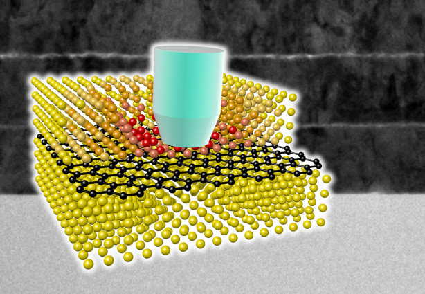 Ultra-High Strength Metamaterial Developed Using Graphene
New metamaterial has been developed, exhibiting hundreds of times greater strength than pure metals.
Professor Seung Min, Han and Yoo Sung, Jeong (Graduate School of Energy, Environment, Water, and Sustainability (EEWS)) and Professor Seok Woo, Jeon (Department of Material Science and Engineering) have developed a composite nanomaterial. The nanomaterial consists of graphene inserted in copper and nickel and exhibits strengths 500 times and 180 times, respectively, greater than that of pure metals. The result of the research was published on the July 2nd online edition in Nature Communications journal.
Graphene displays strengths 200 times greater than that of steel, is stretchable, and is flexible. The U.S. Army Armaments Research, Development and Engineering Center developed a graphene-metal nanomaterial but failed to drastically improve the strength of the material.
To maximize the strength increased by the addition of graphene, the KAIST research team created a layered structure of metal and graphene. Using CVD (Chemical Vapor Deposition), the team grew a single layer of graphene on a metal deposited substrate and then deposited another metal layer. They repeated this process to produce a metal-graphene multilayer composite material, utilizing a single layer of graphene. Micro-compression tests within Transmission Electronic Microscope and Molecular Dynamics simulations effectively showed the strength enhancing effect and the dislocation movement in grain boundaries of graphene on an atomic level.
The mechanical characteristics of the graphene layer within the metal-graphene composite material successfully blocked the dislocations and cracks from external damage from traveling inwards. Therefore the composite material displayed strength beyond conventional metal-metal multilayer materials. The copper-graphene multilayer material with an interplanar distance of 70nm exhibited 500 times greater (1.5GPa) strength than pure copper. Nickel-graphene multilayer material with an interplanar distance of 100nm showed 180 times greater (4.0GPa) strength than pure nickel.
It was found that there is a clear relationship between the interplanar distance and the strength of the multilayer material. A smaller interplanar distance made the dislocation movement more difficult and therefore increased the strength of the material. Professor Han, who led the research, commented, “the result is astounding as 0.00004% in weight of graphene increased the strength of the materials by hundreds of times” and “improvements based on this success, especially mass production with roll-to-roll process or metal sintering process in the production of ultra-high strength, lightweight parts for automobile and spacecraft, may become possible.” In addition, Professor Han mentioned that “the new material can be applied to coating materials for nuclear reactor construction or other structural materials requiring high reliability.”
The research project received support from National Research Foundation, Global Frontier Program, KAIST EEWS-KINC Program and KISTI Supercomputer and was a collaborative effort with KISTI (Korea Institute of Science and Technology Information), KBSI (Korea Basic Science Institute), Stanford University, and Columbia University.
A schematic diagram shows the structure of metal-graphene multi-layers. The metal-graphene multi-layered composite materials, containing a single-layered graphene, block the dislocation movement of graphene layers, resulting in a greater strength in the materials.
2013.08.23 View 16932
Ultra-High Strength Metamaterial Developed Using Graphene
New metamaterial has been developed, exhibiting hundreds of times greater strength than pure metals.
Professor Seung Min, Han and Yoo Sung, Jeong (Graduate School of Energy, Environment, Water, and Sustainability (EEWS)) and Professor Seok Woo, Jeon (Department of Material Science and Engineering) have developed a composite nanomaterial. The nanomaterial consists of graphene inserted in copper and nickel and exhibits strengths 500 times and 180 times, respectively, greater than that of pure metals. The result of the research was published on the July 2nd online edition in Nature Communications journal.
Graphene displays strengths 200 times greater than that of steel, is stretchable, and is flexible. The U.S. Army Armaments Research, Development and Engineering Center developed a graphene-metal nanomaterial but failed to drastically improve the strength of the material.
To maximize the strength increased by the addition of graphene, the KAIST research team created a layered structure of metal and graphene. Using CVD (Chemical Vapor Deposition), the team grew a single layer of graphene on a metal deposited substrate and then deposited another metal layer. They repeated this process to produce a metal-graphene multilayer composite material, utilizing a single layer of graphene. Micro-compression tests within Transmission Electronic Microscope and Molecular Dynamics simulations effectively showed the strength enhancing effect and the dislocation movement in grain boundaries of graphene on an atomic level.
The mechanical characteristics of the graphene layer within the metal-graphene composite material successfully blocked the dislocations and cracks from external damage from traveling inwards. Therefore the composite material displayed strength beyond conventional metal-metal multilayer materials. The copper-graphene multilayer material with an interplanar distance of 70nm exhibited 500 times greater (1.5GPa) strength than pure copper. Nickel-graphene multilayer material with an interplanar distance of 100nm showed 180 times greater (4.0GPa) strength than pure nickel.
It was found that there is a clear relationship between the interplanar distance and the strength of the multilayer material. A smaller interplanar distance made the dislocation movement more difficult and therefore increased the strength of the material. Professor Han, who led the research, commented, “the result is astounding as 0.00004% in weight of graphene increased the strength of the materials by hundreds of times” and “improvements based on this success, especially mass production with roll-to-roll process or metal sintering process in the production of ultra-high strength, lightweight parts for automobile and spacecraft, may become possible.” In addition, Professor Han mentioned that “the new material can be applied to coating materials for nuclear reactor construction or other structural materials requiring high reliability.”
The research project received support from National Research Foundation, Global Frontier Program, KAIST EEWS-KINC Program and KISTI Supercomputer and was a collaborative effort with KISTI (Korea Institute of Science and Technology Information), KBSI (Korea Basic Science Institute), Stanford University, and Columbia University.
A schematic diagram shows the structure of metal-graphene multi-layers. The metal-graphene multi-layered composite materials, containing a single-layered graphene, block the dislocation movement of graphene layers, resulting in a greater strength in the materials.
2013.08.23 View 16932 -
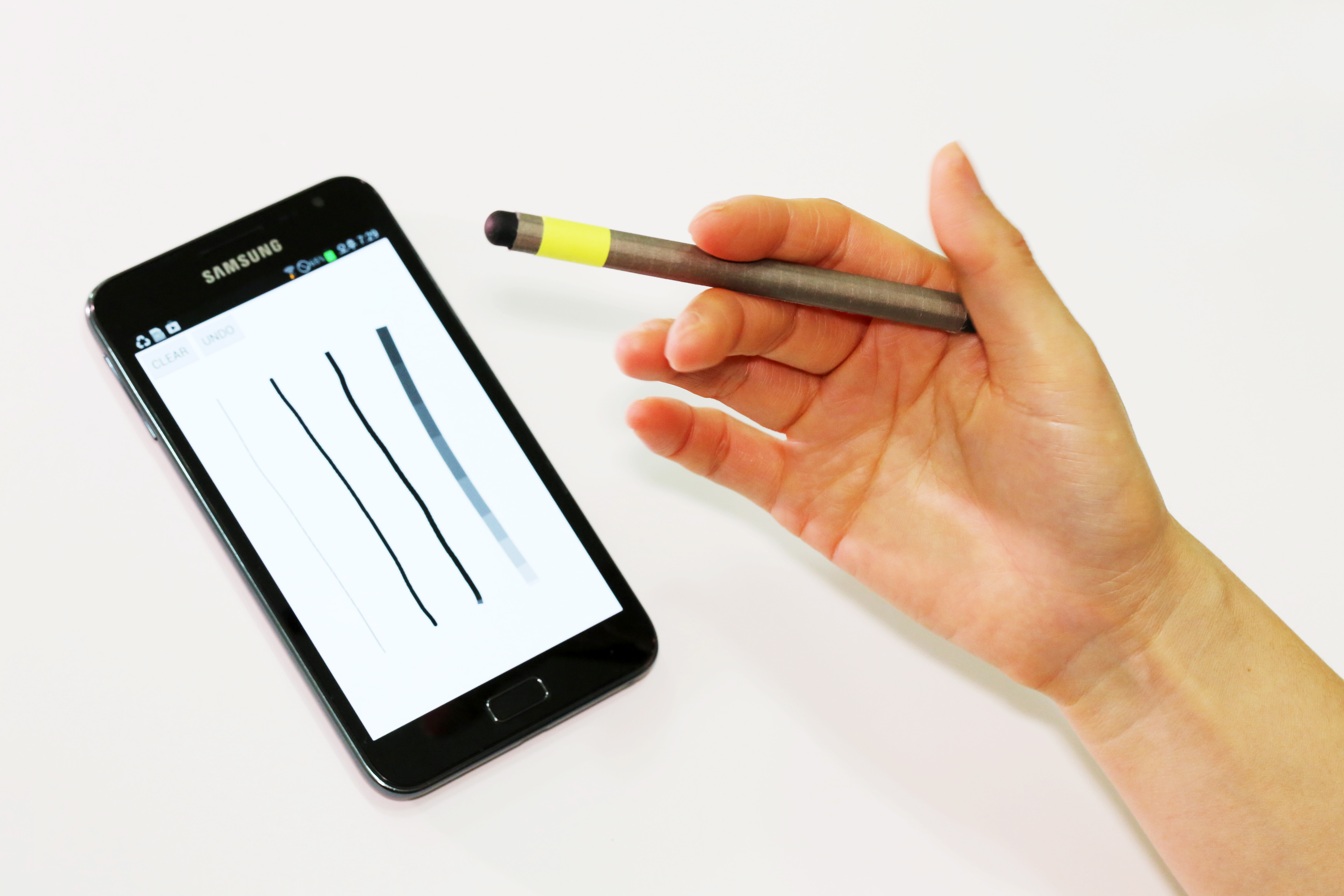 A magnetic pen for smartphones adds another level of conveniences
Utilizing existing features on smartphones, the MagPen provides users with a compatible and simple input tool regardless of the type of phones they are using.
A doctoral candidate at the Korea Advanced Institute of Science and Technology (KAIST) developed a magnetically driven pen interface that works both on and around mobile devices. This interface, called the MagPen, can be used for any type of smartphones and tablet computers so long as they have magnetometers embedded in.
Advised by Professor Kwang-yun Wohn of the Graduate School of Culture Technology (GSCT) at KAIST, Sungjae Hwang, a Ph.D. student, created the MagPen in collaboration with Myung-Wook Ahn, a master"s student at the GSCT of KAIST, and Andrea Bianchi, a professor at Sungkyunkwan University.
Almost all mobile devices today provide location-based services, and magnetometers are incorporated in the integrated circuits of smartphones or tablet PCs, functioning as compasses. Taking advantage of built-in magnetometers, Hwang"s team came up with a technology that enabled an input tool for mobile devices such as a capacitive stylus pen to interact more sensitively and effectively with the devices" touch screen. Text and command entered by a stylus pen are expressed better on the screen of mobile devices than those done by human fingers.
The MagPen utilizes magnetometers equipped with smartphones, thus there is no need to build an additional sensing panel for a touchscreen as well as circuits, communication modules, or batteries for the pen. With an application installed on smartphones, it senses and analyzes the magnetic field produced by a permanent magnet embedded in a standard capacitive stylus pen.
Sungjae Hwang said, "Our technology is eco-friendly and very affordable because we are able to improve the expressiveness of the stylus pen without requiring additional hardware beyond those already installed on the current mobile devices. The technology allows smartphone users to enjoy added convenience while no wastes generated."
The MagPen detects the direction at which a stylus pen is pointing; selects colors by dragging the pen across smartphone bezel; identifies pens with different magnetic properties; recognizes pen-spinning gestures; and estimates the finger pressure applied to the pen.
Notably, with its spinning motion, the MagPen expands the scope of input gestures recognized by a stylus pen beyond its existing vocabularies of gestures and techniques such as titling, hovering, and varying pressures. The tip of the pen switches from a pointer to an eraser and vice versa when spinning. Or, it can choose the thickness of the lines drawn on a screen by spinning.
"It"s quite remarkable to see that the MagPen can understand spinning motion. It"s like the pen changes its living environment from two dimensions to three dimensions. This is the most creative characteristic of our technology," added Sungjae Hwang.
Hwang"s initial research result was first presented at the International Conference on Intelligent User Interfaces organized by the Association for Computing Machinery and held on March 19-22 in Santa Monica, the US.
In the next month of August, the research team will present a paper on the MagPen technology, entitled "MagPen: Magnetically Driven Pen Interaction On and Around Conventional Smartphones" and receive an Honorable Mention Award at the 15th International Conference on Human-Computer Interaction with Mobile Devices and Services (MobileHCI 2013) to be held in Germany.
In addition to the MagPen, Hwang and his team are conducting other projects to develop different types of magnetic gadgets (collectively called "MagGetz") that include the Magnetic Marionette, a magnetic cover for a smartphone, which offers augmented interactions with the phone, as well as magnetic widgets such as buttons and toggle interface.
Hwang has filed ten patents for the MagGetz technology.
Youtube Links: http://www.youtube.com/watch?v=NkPo2las7wc, http://www.youtube.com/watch?v=J9GtgyzoZmM
2013.07.25 View 11915
A magnetic pen for smartphones adds another level of conveniences
Utilizing existing features on smartphones, the MagPen provides users with a compatible and simple input tool regardless of the type of phones they are using.
A doctoral candidate at the Korea Advanced Institute of Science and Technology (KAIST) developed a magnetically driven pen interface that works both on and around mobile devices. This interface, called the MagPen, can be used for any type of smartphones and tablet computers so long as they have magnetometers embedded in.
Advised by Professor Kwang-yun Wohn of the Graduate School of Culture Technology (GSCT) at KAIST, Sungjae Hwang, a Ph.D. student, created the MagPen in collaboration with Myung-Wook Ahn, a master"s student at the GSCT of KAIST, and Andrea Bianchi, a professor at Sungkyunkwan University.
Almost all mobile devices today provide location-based services, and magnetometers are incorporated in the integrated circuits of smartphones or tablet PCs, functioning as compasses. Taking advantage of built-in magnetometers, Hwang"s team came up with a technology that enabled an input tool for mobile devices such as a capacitive stylus pen to interact more sensitively and effectively with the devices" touch screen. Text and command entered by a stylus pen are expressed better on the screen of mobile devices than those done by human fingers.
The MagPen utilizes magnetometers equipped with smartphones, thus there is no need to build an additional sensing panel for a touchscreen as well as circuits, communication modules, or batteries for the pen. With an application installed on smartphones, it senses and analyzes the magnetic field produced by a permanent magnet embedded in a standard capacitive stylus pen.
Sungjae Hwang said, "Our technology is eco-friendly and very affordable because we are able to improve the expressiveness of the stylus pen without requiring additional hardware beyond those already installed on the current mobile devices. The technology allows smartphone users to enjoy added convenience while no wastes generated."
The MagPen detects the direction at which a stylus pen is pointing; selects colors by dragging the pen across smartphone bezel; identifies pens with different magnetic properties; recognizes pen-spinning gestures; and estimates the finger pressure applied to the pen.
Notably, with its spinning motion, the MagPen expands the scope of input gestures recognized by a stylus pen beyond its existing vocabularies of gestures and techniques such as titling, hovering, and varying pressures. The tip of the pen switches from a pointer to an eraser and vice versa when spinning. Or, it can choose the thickness of the lines drawn on a screen by spinning.
"It"s quite remarkable to see that the MagPen can understand spinning motion. It"s like the pen changes its living environment from two dimensions to three dimensions. This is the most creative characteristic of our technology," added Sungjae Hwang.
Hwang"s initial research result was first presented at the International Conference on Intelligent User Interfaces organized by the Association for Computing Machinery and held on March 19-22 in Santa Monica, the US.
In the next month of August, the research team will present a paper on the MagPen technology, entitled "MagPen: Magnetically Driven Pen Interaction On and Around Conventional Smartphones" and receive an Honorable Mention Award at the 15th International Conference on Human-Computer Interaction with Mobile Devices and Services (MobileHCI 2013) to be held in Germany.
In addition to the MagPen, Hwang and his team are conducting other projects to develop different types of magnetic gadgets (collectively called "MagGetz") that include the Magnetic Marionette, a magnetic cover for a smartphone, which offers augmented interactions with the phone, as well as magnetic widgets such as buttons and toggle interface.
Hwang has filed ten patents for the MagGetz technology.
Youtube Links: http://www.youtube.com/watch?v=NkPo2las7wc, http://www.youtube.com/watch?v=J9GtgyzoZmM
2013.07.25 View 11915 -
 Late Dr. Ryu Geun Chul's Achievements and Generous Contributions
First Doctor in the field of Korean Traditional Medicine
The late Dr. Ryu was born in 1926 and is the father figure of Korea’s Traditional Medicine and is its First Doctor (1976 Kyung Hee University), and was the vice-professor of Kyung Hee University of Medicine, Vice-Director of Kyung Hee Institute of Korean Traditional Medicine, and was the first chairman of the Association of Korea Oriental Medicine. He developed the painless acupuncture administering device for the first time in Korea in 1962, and succeeded in anesthetizing a patient for cesarean procedure using acupuncture in 1972.
He even was the first to receive a medical engineering doctorate degree from the Moscow National Engineering School in April of 1996 and developed a stroke rehabilitation machine.
Korea’s Most Generous Donor
Dr. Ryu surprised the world by donating 57.8billion Won worth of real estate to KAIST in August of 2008. Dr. Ryu revealed that his reason for donating such a huge sum to KAIST was due to its focused students giving him the belief that the future of Korea is at KAIST and that the development of science and technology is necessary for Korea to develop into a world class nation and KAIST is the institute most suitable to lead Korea in the field.
Dr. Ryu lived on KAIST campus after donating his entire fortune and even established ‘KAIST scholars and spacemen health research center’ and ‘Dr. Ryu Health Clinic’ as he also wanted to donate his knowledge.
Even when he was a professor at Moscow National Engineering University in the late 1990s he carried out free medical work throughout Korea and in recognition of his devoted work, he was named honorary citizen from Chun Ahn city, San Chung city, and DaeJeon city. In 2007 he donated 450million Won to Cheon Dong Elementary School in Chun Ahn city to build a gymnasium and an indoor golf practice range.
Role as Science and Technology Public Relations Officer
Dr. Ryu volunteered to numerous lectures and interviews after donation to advertise science and technology. His belief that the development of science and technology is necessary for Korea’s development was the driving force behind his efforts at increasing interest and support for the field of science and technology.
In addition, through interviews with MBC, KBS, SBS, KTV, Joong Ang Newspapers, Dong Ah Newspaper and other media mediums, Dr. Ryu improved the public perception on donations whilst increasing the pride of scientists and researchers by highlighting their importance and the importance of science and technology.
In recognition of Dr. Ryu’s efforts, he received the 43rd Science Day Science and Technology Creation Award, 2010 MBC Social Service Special Award, and 2010 ‘Proud Chung Cheong Citizen’ Award.
2011.03.22 View 19043
Late Dr. Ryu Geun Chul's Achievements and Generous Contributions
First Doctor in the field of Korean Traditional Medicine
The late Dr. Ryu was born in 1926 and is the father figure of Korea’s Traditional Medicine and is its First Doctor (1976 Kyung Hee University), and was the vice-professor of Kyung Hee University of Medicine, Vice-Director of Kyung Hee Institute of Korean Traditional Medicine, and was the first chairman of the Association of Korea Oriental Medicine. He developed the painless acupuncture administering device for the first time in Korea in 1962, and succeeded in anesthetizing a patient for cesarean procedure using acupuncture in 1972.
He even was the first to receive a medical engineering doctorate degree from the Moscow National Engineering School in April of 1996 and developed a stroke rehabilitation machine.
Korea’s Most Generous Donor
Dr. Ryu surprised the world by donating 57.8billion Won worth of real estate to KAIST in August of 2008. Dr. Ryu revealed that his reason for donating such a huge sum to KAIST was due to its focused students giving him the belief that the future of Korea is at KAIST and that the development of science and technology is necessary for Korea to develop into a world class nation and KAIST is the institute most suitable to lead Korea in the field.
Dr. Ryu lived on KAIST campus after donating his entire fortune and even established ‘KAIST scholars and spacemen health research center’ and ‘Dr. Ryu Health Clinic’ as he also wanted to donate his knowledge.
Even when he was a professor at Moscow National Engineering University in the late 1990s he carried out free medical work throughout Korea and in recognition of his devoted work, he was named honorary citizen from Chun Ahn city, San Chung city, and DaeJeon city. In 2007 he donated 450million Won to Cheon Dong Elementary School in Chun Ahn city to build a gymnasium and an indoor golf practice range.
Role as Science and Technology Public Relations Officer
Dr. Ryu volunteered to numerous lectures and interviews after donation to advertise science and technology. His belief that the development of science and technology is necessary for Korea’s development was the driving force behind his efforts at increasing interest and support for the field of science and technology.
In addition, through interviews with MBC, KBS, SBS, KTV, Joong Ang Newspapers, Dong Ah Newspaper and other media mediums, Dr. Ryu improved the public perception on donations whilst increasing the pride of scientists and researchers by highlighting their importance and the importance of science and technology.
In recognition of Dr. Ryu’s efforts, he received the 43rd Science Day Science and Technology Creation Award, 2010 MBC Social Service Special Award, and 2010 ‘Proud Chung Cheong Citizen’ Award.
2011.03.22 View 19043 -
Professor Min Beom Ki develops metamaterial with high index of refraction
Korean research team was able to theoretically prove that a metamaterial with high index of refraction does exist and produced it experimentally.
Professor Min Beom Ki, Dr. Choi Moo Han, and Doctorate candidate Lee Seung Hoon was joined by Dr. Kang Kwang Yong’s team from ETRI, KAIST’s Professor Less Yong Hee’s team, and Seoul National University’s Professor Park Nam Kyu’s team. The research was funded by the Basic Research Support Program initiated by the Ministry of Education, Science, and Technology and Korea Research Federation.
The result of the research was published in ‘Nature’ magazine and is one of the few researches carried out by teams composed entirely of Koreans.
Metamaterials are materials that have physical properties beyond those materials’ properties that are found in nature. It is formed not with atoms, but with synthetic atoms which have smaller structures than wavelengths.
The optical and electromagnetic waves’ properties of metamaterials can be altered significantly which has caught the attention of scientists worldwide.
Professor Min Beom Ki’s team independently designed and created a dielectric metamaterial with high polarization and low diamagnetism with an index of refraction of 38.6, highest synthesized index value.
It is expected that the result of the experiment will help develop high resolution imaging system and ultra small, hyper sensitive optical devices.
2011.02.23 View 18501