CT
-
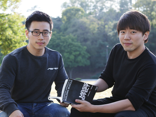 Two Undergraduate KAIST Students Publish a Book on Health Management
Joonho Suh of the Aerospace Engineering Department and Jiho Suh of the Mechanical Engineering Department are both brothers and undergraduates at KAIST.
The Suh brothers, who are three years apart, have recently published a self-help book in English on staying healthy entitled “A Scientific Approach to Building Muscle: Mass Effect.”
The book introduces techniques to build muscles, adapting them from an engineering concept called "Active Torque Control (ACT)," the management of turning forces imposed on a vehicle. Just as ACT influences the performance of a vehicle, good exercise involves the right degree of body angles and the right direction of body movements to keep the best posture necessary for burning calories and strengthening muscles.
In the book, they also suggest healthy diet plans based on scientific knowledge and data that the writers borrowed from such fields as anatomy, physiology, and motor mechanics to maintain a healthy weight.
Joonho Suh said,
“If we understand the mechanism of how our body works, the chances are high we will have good muscle tone and a balanced diet. We used a great deal of scientific knowledge and turned it into a health management program that can be customized per individual needs.”
The younger brother, Jiho, added,
“In fact, we applied our methods in the book to beginners who took weight training and fitness for one hour a day for one month, we learned that their muscle mass increased by 1-1.5 kg while losing body fat by 2-3 kg.”
The brothers said they planned to publish a Korean language version of the book next year.
The authors of "Mass Effect": Joonho Suh (left) and Jiho Suh (right)
2015.10.26 View 7914
 -
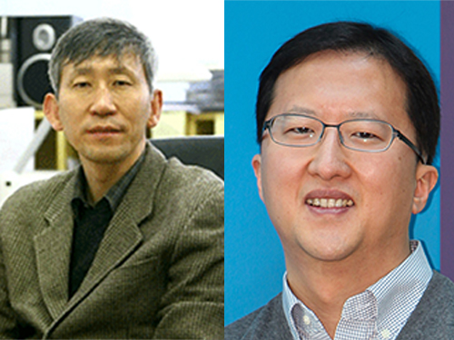 Professors Sukbok Chang and Jang-Wook Choi Receive the 2015 Knowledge Award from the Korean Government
The Ministry of Science, ICT and Future Planning (MISP) of the Republic of Korea announced the 2015 Knowledge Awards on October 20, 2015. Two KAIST professors received the award.
Established in 2009, the awards are presented to Korean scientists whose publications have contributed to the international science community. Specifically, the MISP used the two biggest science databases, Science Citation Index Expanded (SCIE) and Scopus, to identify ten highly cited papers ranked in the top 1% by total citations in the past ten years.
Professor Sukbok Chang of Chemistry (left in the picture below) is a global authority in the field of catalytic hydrocarbon functionalization. His paper entitled “Palladium-catalyzed C-H Functionalization of Pyridine N-Oxides: Highly Selective Alkenylation and Direct Arylation with Unactivated Arenes,” which was published in the Journal of the American Chemical Society in 2008, was once selected by Thomson Reuters as one of the “Most Influential Research Papers of the Month.” In 2011, the American Chemical Society included his paper in the list of the top 20 research papers that were most frequently cited in the last three years.
Professor Jang-Wook Choi of the Graduate School of EEWS (Energy, Environment, Water, and Sustainability) has been known for his leading research in rechargeable battery, supercapacitor, and materials chemistry. In particular, his work on secondary fuel cells attracted significant attention from academia and industry in Korea. Professor Choi developed a super-thin flexible lithium-ion battery this year, thinner than a credit card, which lasts longer than the existing batteries and with greater performance. He also developed new electrode materials for next-generation sodium-ion and magnesium secondary fuel cells.
Professor Sukbok Chang (left) and Professor Jang-Wook Choi (right)
2015.10.23 View 12544
 -
 Establishment of System Metabolic Engineering Strategies
Although conventional petrochemical processes have generated chemicals and materials which have been useful to mankind, they have also triggered a variety of environmental problems including climate change and relied too much on nonrenewable natural resources. To ameliorate this, researchers have actively pursued the development of industrial microbial strains around the globe in order to overproduce industrially useful chemicals and materials from microbes using renewable biomass. This discipline is called metabolic engineering.
Thanks to advances in genetic engineering and our knowledge of cellular metabolism, conventional metabolic engineering efforts have succeeded to a certain extent in developing microbial strains that overproduce bioproducts at an industrial level. However, many metabolic engineering projects launched in academic labs do not reach commercial markets due to a failure to fully integrate industrial bioprocesses.
In response to this, Distinguished Professor Sang Yup Lee and Dr. Hyun Uk Kim, both from the Department of Chemical and Biomolecular Engineering at KAIST, have recently suggested ten general strategies of systems metabolic engineering to successfully develop industrial microbial strains. Systems metabolic engineering differs from conventional metabolic engineering by incorporating traditional metabolic engineering approaches along with tools of other fields, such as systems biology, synthetic biology, and molecular evolution.
The ten strategies of systems metabolic engineering have been featured in Nature Biotechnology released online in October 2015, which is entitled "Systems strategies for developing industrial microbial strains."
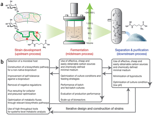
The strategies cover economic, state-of-the-art biological techniques and traditional bioprocess aspects. Specifically, they consist of: 1) project design including economic evaluation of a target bioproduct; 2) selection of host strains to be used for overproduction of a bioproduct; 3) metabolic pathway reconstruction for bioproducts that are not naturally produced in the selected host strains; 4) increasing tolerance of a host strain against the bioproduct; 5) removing negative regulatory circuits in the microbial host limiting overproduction of a bioproduct; 6) rerouting intracellular fluxes to optimize cofactor and precursor availability necessary for the bioproduct formation; 7) diagnosing and optimizing metabolic fluxes towards product formation; 8) diagnosis and optimization of microbial culture conditions including carbon sources; 9) system-wide gene manipulation to further increase the host strain's production performance using high-throughput genome-scale engineering and computational tools; and 10) scale-up fermentation of the developed strain and diagnosis for the reproducibility of the strain's production performance.
These ten strategies were articulated with successful examples of the production of L-arginine using Corynebacterium glutamicum, 1,4-butanediol using Escherichia coli, and L-lysine and bio-nylon using C. glutamicum.
Professor Sang Yup Lee said, "At the moment, the chance of commercializing microbial strains developed in academic labs is very low. The strategies of systems metabolic engineering outlined in this analysis can serve as guidelines when developing industrial microbial strains. We hope that these strategies contribute to improving opportunities to commercialize microbial strains developed in academic labs with drastically reduced costs and efforts, and that a large fraction of petroleum-based processes will be replaced with sustainable bioprocesses."
Lee S. Y. & Kim, H. U. Systems Strategies for Developing Industrial Microbial Strains. Nature Biotechnology (2015).
This work was supported by the Technology Development Program to Solve Climate Change on Systems Metabolic Engineering for Biorefineries (NRF-2012M1A2A2026556) and by the Intelligent Synthetic Biology Center through the Global Frontier Project (2011-0031963) from the Ministry of Science, ICT and Future Planning (MSIP), Korea, and through the National Research Foundation (NRF) of Korea. This work was also supported by the Novo Nordisk Foundation.
Picture: Concept of the Systems Metabolic Engineering Framework
(a) Three major bioprocess stages (b) Considerations in systems metabolic engineering to optimize the whole bioprocess. List of considerations for the strain development and fermentation contribute to improving microbial strain's production performance (red), whereas those for the separation and purification help in reducing overall operation costs by facilitating the downstream process (blue). Some of the considerations can be repeated in the course of systems metabolic engineering.
2015.10.19 View 11235
 -
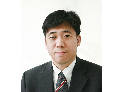 Professor Ki-Jun Jeong Wins the 2015 Dam Yeun Academic Award
The 11th Dam Yeun Academic Award presented by the Korean Society for Biotechnology and Bioengineering (KSBB) to a biologist under 45 years old went to Professor Ki-Jun Jeong of the Chemical and Biomolecular Engineering Department at KAIST.
The award ceremony took place on October 13, 2015, at the annual conference of KSBB held at Songdo Convensia in Incheon City.
Each year KSBB announces the recipient of the award based on the publications by researchers in the last five years at peer-reviewed international journals or KSBB Journal as well as the record of patent registration and technology transfers.
Professor Jeong is recognized for his pioneering research in protein, antibody, cellular engineering, and protein displays and chips.
2015.10.19 View 9674
 -
 KAIST's College of Business Places Fourth in the 2015 Better World MBA Ranking
The Corporate Knights, a business and society magazine based in Canada, released the results of the 2015 Better World MBA Ranking on October 8, 2015.
KAIST’s business school ranked fourth globally and, number one in Asia, according to the list.
The 2015 Corporate Knights Better World MBA Ranking included a total of 121 schools; York University’s Schulich School of Business of Canada took first place.
The rankings were based on three criteria: the number of curricula (core and required courses) dedicated to sustainability, the number of research institutions and centers at the business school, and the volume of faculty research focused on better world topics such as sustainable finance, clean energy, or gender diversity.
The Better World MBA Ranking aims to identify business schools that best equip graduates who seek to change the world for the better by offering students opportunities to learn how to integrate social and environmental factors in their understanding of management functions via core MBA courses, faculty expertise, and research centers.
Dean Dong-Seok Kim of the College of Business at KAIST said,
“For years, our school has introduced a wide range of programs and research initiatives that address important social needs and issues. As part of this effort, we created the Graduate School of Green Growth and MBA for Social Entrepreneurship back in 2013. I believe that these endeavors played a favorable role in our receiving high scores in the ranking.”
KAIST’s Graduate School of Green Growth previously ranked sixth in the world’s top Green MBA School list published by Corporate Knights.
For the 2015 Better World MBA Ranking, go to
http://www.corporateknights.com/reports/2015-global-sustainable-mba/11153-14442629/.
2015.10.12 View 5638
 -
 Professor Sang-Min Bae receives the 2015 IDEA Awards
Professor Sang-min Bae of the Industrial Design Department at KAIST garnered one silver and two bronze awards from the 2015 International Design Excellence Awards (IDEA). Along with iF Design Award and Red Dot Design Awards, the IDEA is regarded as one of the world’s most respected recognition in the field of design.
Trash to Bin (T2B), a silver winner in the category of Social Impact Design, is a trash bin made of 1.87 lb (0.85 kg) of discarded papers. Using one-hundred percent recycled paper pulp, each T2B costs under $5 for production. The bin can be fully waterproofed for at least six hours. While satisfying with the industry safety standards, this environmentally-friendly bin can be produced on a large scale using litter energy, but offering the exact same benefit of a general garbage can.
Roll-Di, one of the two bronze winners, is a direction indicator that tells which string of screen curtains should be pulled to make the curtain go up or down. As shown in the picture below, Roll-Di can be installed at the bottom of the string, and the “up and down” arrows show which side of the string needs to be pulled to achieve the desired position of the curtain. This simple, yet handy solution to the problem that people frequently make the mistake of pulling the wrong string provides users with greater convenience.
The other bronze winner is Printing Solar-cell, an organic cartridge module that prints solar-cells using a domestic, ink-jet printer. With Printing Solar-cell, users can design their own cell patterns and charge their electronics anywhere holding the printed solar-cell on a copy paper.
Professor Bae said, “I’ve always tried to design something that is useful for people in need. I consider the IDEA awards an encouragement to keep up with my work toward that goal.”
Trash to Bin
Roll-Di
Printing Solar-cell
2015.09.30 View 8700
 -
 KAIST and Chongqing University of Technology in China Open an International Program
With the help of KAIST, Chongqing University of Technology (CQUT) in China established an electrical engineering and computer science program and admitted their first 66 freshmen this fall semester.
The joint program was created to foster skilled engineers in the fields of electrical engineering and computer science, which are necessary for the development of the Korean and Chinese Industrial Complex located in Chongqing City.
KAIST has provided CQUT with a majority of the program’s curricula currently offered to its students in Daejeon, Korea.
Under the jointly administered program, KAIST takes on education and research while CQUT is responsible for student selection and administration.
KAIST has dispatched eight professors to teach the related fields in English, and 17 CQUT professors will teach the rest of the curricula.
In August 2014, KAIST and CQUT singed a cooperation agreement for education and research exchange and created the CQUT-KAIST Education Cooperation Center, which is headed by Professor Young-Nam Han of the Electrical Engineering Department at KAIST.
The two universities will expand their collaboration to include graduate programs by 2016.
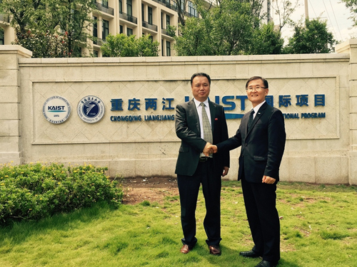
In the picture below, President Steve Kang of KAIST (right) shakes hands with President Shi Xiaohui of Chongqing University of Technology (left).
2015.09.17 View 11107
 -
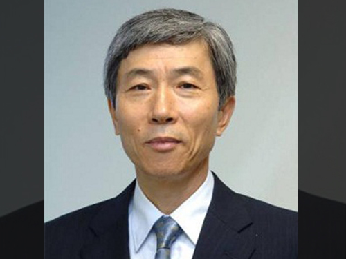 Professor Seok-Jung Kang Is Appointed the Director of the Korea Institute of Ceramic Engineering and Technology
Professor Seok-Jung Kang of the Material Sciences and Engineering Department at KAIST has been appointed to the position of the third Director of the Korea Institute of Ceramic Engineering and Technology. His three-year term will begin September 9, 2015.
An authority in the field of ceramics, Professor Kang has taught at KAIST since 1980. He received his bachelor’s degree from the Department of Metallurgical Engineering at Seoul National University, his master’s degree at KAIST, and his doctoral degree at the Ecole Centrale de Paris.
Professor Kang received the Robert B. Sosman Award in 2011, an annual prize given by the American Society of Ceramics to recognize outstanding achievement in basic science in an area that results in significant impact to the field of ceramics. He was the first Asian recipient of the award.
He also received the 2015 Professor Sir Richard Brooke Award, a prestigious bi-annual prize presented to an outstanding scholar by the European Society of Ceramics.
2015.09.15 View 6918
 -
 Professor Jeong Ho Lee Receives the 2015 Pediatric Epilepsies Research Award
The award identifies leading scientists worldwide and funds their cutting-edge research in epilepsy.
The Citizen United for Research in Epilepsy (CURE) announced on September 7, 2015, that Jeong Ho Lee, a professor of the Graduate School of Medical Science and Engineering at KAIST, will be awarded the 2015 Pediatric Epilepsies Research Award.
The Pediatric Epilepsies Research Award is given annually to a researcher who has conducted novel, innovative research projects that address severe, intractable pediatric epilepsies as well as collaborative, interdisciplinary projects that explore new approaches to find a treatment for pediatric epilepsies.
Lee was recognized for his leading study in the field of intractable epilepsy. He is the first Korean who has ever received this award, securing a research grant of USD 250,000 for two years.
Lee has conducted research on brain somatic mutations as the novel cause of childhood intractable epilepsy. Pediatric epilepsies account for approximately 70% of all cases of epilepsy.
Established in 1998, CURE is a non-profit American organization based in Chicago, Illinois, which is committed to funding research and various initiatives that will lead to breakthroughs to cure epilepsy.
Since its inception, CURE has been at the forefront of epilepsy research, raising more than USD 32 million to support researchers and scientists worldwide. It has also awarded more than 180 cutting-edge projects in 13 countries.
2015.09.09 View 11460
 -
 KAIST's Student Job Fair 2015
KAIST’s Undergraduate Student Council and Graduate Student Council jointly hosted the 2015 KAIST Job Fair on September 2-3, 2015 at the Sports Complex on campus.
The Job Fair took place for the sixth time this year. Forty-three companies, including some of the largest ones in Korea such as Samsung, Hyundai, LG, SK Construction, Hankook Tires, as well as those owned by KAIST graduates, have participated.
The Job Fair specialized in three fields: information technology (IT) and electronic and mechanical engineering. The event included one-to-one employment counseling between human resources managers and students, mock interviews, employment orientations, job consulting, interview makeup lessons, resume writing and photo-shooting, etc.
The international students who attended the event received information packages on employment from the participating companies.
This event was open not only to KAIST students but also to students from other universities in the local community, offering more job opportunities to a wider range of people.
Last year alone, a total of 1,200 people including KAIST students and graduates joined the KAIST’s Job Fair.
2015.09.04 View 6740
 -
 KAIST's Research Team Receives the Best Paper Award from the IEEE Transaction on Power Electronics
A research team led by Professor Chun T. Rim of the Department of Nuclear and Quantum Engineering at the Korea Advanced Institute of Science and Technology (KAIST) has received the First Prize Papers Award from the IEEE (Institute of Electrical and Electronics Engineers) Transactions on Power Electronics (TPEL), a peer-reviewed journal that covers fundamental technologies used in the control and conversion of electric power.
A total of three research papers received this award in 2015.
Each year, TPEL’s editors select three best papers among those published in the journal during the preceding calendar year. In 2014, the TPEL published 579 papers. Professor Rim’s paper was picked out as one of the three papers published last year for the First Prize Papers Award.
Entitled “Generalized Active EMF (electromagnetic field) Cancel Methods for Wireless Electric Vehicles (http://ieeexplore.ieee.org/xpls/abs_all.jsp?arnumber=6684288&tag=1),” the paper proposed, for the first time in the world, three generalized design methods for cancelling the total EMF generated from wireless electric vehicles. This technology, researchers said, can be applied to any wireless power transfer systems.
The award ceremony will be held at the upcoming conference of the 2015 IEEE Energy Conversion Congress and Expo in September in Montreal, Canada.
2015.08.27 View 11092
 -
 'Engineered Bacterium Produces 1,3-Diaminopropane'
A research team led by Distinguished Professor Sang Yup Lee of the Department of Chemical and Biomolecular Engineering at KAIST reported, for the first time, the production of 1,3-diaminopropane via fermentation of an engineered bacterium.
1,3-Diaminopropane is a three carbon diamine, which has a wide range of industrial applications including epoxy resin and cross-linking agents, as well as precursors for pharmaceuticals, agrochemicals, and organic chemicals. It can also be polymerized with dicarboxylic acids to make polyamides (nylons) for use as engineering plastics, medical materials, and adhesives.
Traditionally, 1,3-diaminopropane is derived from petroleum-based processes. In effort to address critical problems such as the depletion of petroleum and environmental issues inherent to the petroleum-based processes, the research team has developed an Escherichia coli (E. coli) strain capable of producing 1,3-diaminopropane. Using this technology, 1,3-diaminopropane can now be produced from renewable biomass instead of petroleum.
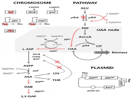
E. coli as found in nature is unable to produce 1,3-diaminopropane. Metabolic engineering, a technology to transform microorganisms into highly efficient microbial cell factories capable of producing chemical compounds of interest, was utilized to engineer the E. coli strain. First, naturally existing metabolic pathways for the biosynthesis of 1,3-diaminopropane were introduced into a virtual cell in silico to determine the most efficient metabolic pathway for the 1,3-diaminopropane production. The metabolic pathway selected was then introduced into an E. coli strain and successfully produced 1,3-diaminopropane for the first time in the world.
The research team applied metabolic engineering additionally, and the production titer of 1,3-diaminopropane increased about 21 fold. The Fed-batch fermentation of the engineered E. coli strain produced 13 grams per liter of 1,3-diaminoproapne. With this technology, 1,3-diaminopropane can be produced using renewable biomass, and it will be the starting point for replacing the current petroleum-based processes with bio-based processes.
Professor Lee said, “Our study suggested a possibility to produce 1,3-diaminopropane based on biorefinery. Further study will be done to increase the titer and productivity of 1,3-diaminopropane.”
This work was published online in Scientific Reports on August 11, 2015.
Reference: Chae, T.U. et al. "Metabolic engineering of Escherichia coli for the production of 1,3-diaminopropane, a three carbon diamine," Scientific Reports:
http://www.nature.com/articles/srep13040
This research was supported by the Technology Development Program to Solve Climate Changes on Systems Metabolic Engineering for Biorefineries from Ministry of Science, ICT and Future Planning (MSIP) through the National Research Foundation (NRF) of Korea.
Figure 1: Metabolic engineering strategies for 1,3-diaminopropane production using C4 pathway
Figure 2: Fed-batch fermentation profiles of two final engineered E. coli strains
2015.08.12 View 11402