electron
-
 Wirelessly Rechargeable Soft Brain Implant Controls Brain Cells
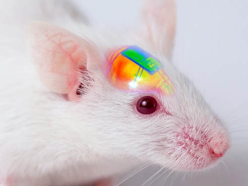
Researchers have invented a smartphone-controlled soft brain implant that can be recharged wirelessly from outside the body. It enables long-term neural circuit manipulation without the need for periodic disruptive surgeries to replace the battery of the implant. Scientists believe this technology can help uncover and treat psychiatric disorders and neurodegenerative diseases such as addiction, depression, and Parkinson’s.
A group of KAIST researchers and collaborators have engineered a tiny brain implant that can be wirelessly recharged from outside the body to control brain circuits for long periods of time without battery replacement. The device is constructed of ultra-soft and bio-compliant polymers to help provide long-term compatibility with tissue. Geared with micrometer-sized LEDs (equivalent to the size of a grain of salt) mounted on ultrathin probes (the thickness of a human hair), it can wirelessly manipulate target neurons in the deep brain using light.
This study, led by Professor Jae-Woong Jeong, is a step forward from the wireless head-mounted implant neural device he developed in 2019. That previous version could indefinitely deliver multiple drugs and light stimulation treatment wirelessly by using a smartphone. For more, Manipulating Brain Cells by Smartphone.
For the new upgraded version, the research team came up with a fully implantable, soft optoelectronic system that can be remotely and selectively controlled by a smartphone. This research was published on January 22, 2021 in Nature Communications.
The new wireless charging technology addresses the limitations of current brain implants. Wireless implantable device technologies have recently become popular as alternatives to conventional tethered implants, because they help minimize stress and inflammation in freely-moving animals during brain studies, which in turn enhance the lifetime of the devices. However, such devices require either intermittent surgeries to replace discharged batteries, or special and bulky wireless power setups, which limit experimental options as well as the scalability of animal experiments.
“This powerful device eliminates the need for additional painful surgeries to replace an exhausted battery in the implant, allowing seamless chronic neuromodulation,” said Professor Jeong. “We believe that the same basic technology can be applied to various types of implants, including deep brain stimulators, and cardiac and gastric pacemakers, to reduce the burden on patients for long-term use within the body.”
To enable wireless battery charging and controls, researchers developed a tiny circuit that integrates a wireless energy harvester with a coil antenna and a Bluetooth low-energy chip. An alternating magnetic field can harmlessly penetrate through tissue, and generate electricity inside the device to charge the battery. Then the battery-powered Bluetooth implant delivers programmable patterns of light to brain cells using an “easy-to-use” smartphone app for real-time brain control.
“This device can be operated anywhere and anytime to manipulate neural circuits, which makes it a highly versatile tool for investigating brain functions,” said lead author Choong Yeon Kim, a researcher at KAIST.
Neuroscientists successfully tested these implants in rats and demonstrated their ability to suppress cocaine-induced behaviour after the rats were injected with cocaine. This was achieved by precise light stimulation of relevant target neurons in their brains using the smartphone-controlled LEDs. Furthermore, the battery in the implants could be repeatedly recharged while the rats were behaving freely, thus minimizing any physical interruption to the experiments.
“Wireless battery re-charging makes experimental procedures much less complicated,” said the co-lead author Min Jeong Ku, a researcher at Yonsei University’s College of Medicine.
“The fact that we can control a specific behaviour of animals, by delivering light stimulation into the brain just with a simple manipulation of smartphone app, watching freely moving animals nearby, is very interesting and stimulates a lot of imagination,” said Jeong-Hoon Kim, a professor of physiology at Yonsei University’s College of Medicine. “This technology will facilitate various avenues of brain research.”
The researchers believe this brain implant technology may lead to new opportunities for brain research and therapeutic intervention to treat diseases in the brain and other organs.
This work was supported by grants from the National Research Foundation of Korea and the KAIST Global Singularity Research Program.
-Profile
Professor Jae-Woong Jeong
https://www.jeongresearch.org/
School of Electrical Engineering
KAIST
2021.01.26 View 28449
Wirelessly Rechargeable Soft Brain Implant Controls Brain Cells
Researchers have invented a smartphone-controlled soft brain implant that can be recharged wirelessly from outside the body. It enables long-term neural circuit manipulation without the need for periodic disruptive surgeries to replace the battery of the implant. Scientists believe this technology can help uncover and treat psychiatric disorders and neurodegenerative diseases such as addiction, depression, and Parkinson’s.
A group of KAIST researchers and collaborators have engineered a tiny brain implant that can be wirelessly recharged from outside the body to control brain circuits for long periods of time without battery replacement. The device is constructed of ultra-soft and bio-compliant polymers to help provide long-term compatibility with tissue. Geared with micrometer-sized LEDs (equivalent to the size of a grain of salt) mounted on ultrathin probes (the thickness of a human hair), it can wirelessly manipulate target neurons in the deep brain using light.
This study, led by Professor Jae-Woong Jeong, is a step forward from the wireless head-mounted implant neural device he developed in 2019. That previous version could indefinitely deliver multiple drugs and light stimulation treatment wirelessly by using a smartphone. For more, Manipulating Brain Cells by Smartphone.
For the new upgraded version, the research team came up with a fully implantable, soft optoelectronic system that can be remotely and selectively controlled by a smartphone. This research was published on January 22, 2021 in Nature Communications.
The new wireless charging technology addresses the limitations of current brain implants. Wireless implantable device technologies have recently become popular as alternatives to conventional tethered implants, because they help minimize stress and inflammation in freely-moving animals during brain studies, which in turn enhance the lifetime of the devices. However, such devices require either intermittent surgeries to replace discharged batteries, or special and bulky wireless power setups, which limit experimental options as well as the scalability of animal experiments.
“This powerful device eliminates the need for additional painful surgeries to replace an exhausted battery in the implant, allowing seamless chronic neuromodulation,” said Professor Jeong. “We believe that the same basic technology can be applied to various types of implants, including deep brain stimulators, and cardiac and gastric pacemakers, to reduce the burden on patients for long-term use within the body.”
To enable wireless battery charging and controls, researchers developed a tiny circuit that integrates a wireless energy harvester with a coil antenna and a Bluetooth low-energy chip. An alternating magnetic field can harmlessly penetrate through tissue, and generate electricity inside the device to charge the battery. Then the battery-powered Bluetooth implant delivers programmable patterns of light to brain cells using an “easy-to-use” smartphone app for real-time brain control.
“This device can be operated anywhere and anytime to manipulate neural circuits, which makes it a highly versatile tool for investigating brain functions,” said lead author Choong Yeon Kim, a researcher at KAIST.
Neuroscientists successfully tested these implants in rats and demonstrated their ability to suppress cocaine-induced behaviour after the rats were injected with cocaine. This was achieved by precise light stimulation of relevant target neurons in their brains using the smartphone-controlled LEDs. Furthermore, the battery in the implants could be repeatedly recharged while the rats were behaving freely, thus minimizing any physical interruption to the experiments.
“Wireless battery re-charging makes experimental procedures much less complicated,” said the co-lead author Min Jeong Ku, a researcher at Yonsei University’s College of Medicine.
“The fact that we can control a specific behaviour of animals, by delivering light stimulation into the brain just with a simple manipulation of smartphone app, watching freely moving animals nearby, is very interesting and stimulates a lot of imagination,” said Jeong-Hoon Kim, a professor of physiology at Yonsei University’s College of Medicine. “This technology will facilitate various avenues of brain research.”
The researchers believe this brain implant technology may lead to new opportunities for brain research and therapeutic intervention to treat diseases in the brain and other organs.
This work was supported by grants from the National Research Foundation of Korea and the KAIST Global Singularity Research Program.
-Profile
Professor Jae-Woong Jeong
https://www.jeongresearch.org/
School of Electrical Engineering
KAIST
2021.01.26 View 28449 -
 Extremely Stable Perovskite Nanoparticles Films for Next-Generation Displays
Researchers have reported an extremely stable cross-linked perovskite nanoparticle that maintains a high photoluminescence quantum yield (PLQY) for 1.5 years in air and harsh liquid environments. This stable material’s design strategies, which addressed one of the most critical problems limiting their practical application, provide a breakthrough for the commercialization of perovskite nanoparticles in next-generation displays and bio-related applications.
According to the research team led by Professor Byeong-Soo Bae, their development can survive in severe environments such as water, various polar solvents, and high temperature with high humidity without additional encapsulation. This development is expected to enable perovskite nanoparticles to be applied to high color purity display applications as a practical color converting material. This result was published as the inside front cover article in Advanced Materials.
Perovskites, which consist of organics, metals, and halogen elements, have emerged as key elements in various optoelectronic applications. The power conversion efficiency of photovoltaic cells based on perovskites light absorbers has been rapidly increased. Perovskites are also great promise as a light emitter in display applications because of their low material cost, facile wavelength tunability, high (PLQY), very narrow emission band width, and wider color gamut than inorganic semiconducting nanocrystals and organic emitters. Thanks to these advantages, perovskites have been identified as a key color-converting material for next-generation high color-purity displays. In particular, perovskites are the only luminescence material that meets Rec. 2020 which is a new color standard in display industry.
However, perovskites are very unstable against heat, moisture, and light, which makes them almost impossible to use in practical applications. To solve these problems, many researchers have attempted to physically prevent perovskites from coming into contact with water molecules by passivating the perovskite grain and nanoparticle surfaces with organic ligands or inorganic shell materials, or by fabricating perovskite-polymer nanocomposites. These methods require complex processes and have limited stability in ambient air and water. Furthermore, stable perovskite nanoparticles in the various chemical environments and high temperatures with high humidity have not been reported yet.
The research team in collaboration with Seoul National University develops siloxane-encapsulated perovskite nanoparticle composite films. Here, perovskite nanoparticles are chemically crosslinked with thermally stable siloxane molecules, thereby significantly improving the stability of the perovskite nanoparticles without the need for any additional protecting layer.
Siloxane-encapsulated perovskite nanoparticle composite films exhibited a high PLQY (> 70%) value, which can be maintained over 600 days in water, various chemicals (alcohol, strong acidic and basic solutions), and high temperatures with high humidity (85℃/85%). The research team investigated the mechanisms impacting the chemical crosslinking and water molecule-induced stabilization of perovskite nanoparticles through various photo-physical analysis and density-functional theory calculation.
The research team confirmed that displays based on their siloxane-perovskite nanoparticle composite films exhibited higher PLQY and a wider color gamut than those of Cd-based quantum dots and demonstrated perfect color converting properties on commercial mobile phone screens. Unlike what was commonly believed in the halide perovskite field, the composite films showed excellent bio-compatibility because the siloxane matrix prevents the toxicity of Pb in perovskite nanoparticle.
By using this technology, the instability of perovskite materials, which is the biggest challenge for practical applications, is greatly improved through simple encapsulation method.
“Perovskite nanoparticle is the only photoluminescent material that can meet the next generation display color standard. Nevertheless, there has been reluctant to commercialize it due to its moisture vulnerability. The newly developed siloxane encapsulation technology will trigger more research on perovskite nanoparticles as color conversion materials and will accelerate early commercialization,” Professor Bae said.
This work was supported by the Wearable Platform Materials Technology Center (WMC) of the Engineering Research Center (ERC) Project, and the Leadership Research Program funded by the National Research Foundation of Korea.
-Publication:
Junho Jang, Young-Hoon Kim, Sunjoon Park, Dongsuk Yoo, Hyunjin Cho, Jinhyeong Jang, Han Beom Jeong, Hyunhwan Lee, Jong Min Yuk, Chan Beum Park, Duk Young Jeon, Yong-Hyun Kim, Byeong-Soo Bae, and Tae-Woo Lee. “Extremely Stable Luminescent Crosslinked Perovskite Nanoparticles under Harsh Environments over 1.5 Years” Advanced Materials, 2020, 2005255. https://doi.org/10.1002/adma.202005255.
Link to download the full-text paper:
https://onlinelibrary.wiley.com/doi/10.1002/adma.202005255
-Profile: Prof. Byeong-Soo Bae (Corresponding author)
bsbae@kaist.ac.kr
Lab. of Optical Materials & Coating
Department of Materials Science and Engineering
Korea Advanced Institute of Science and Technology (KAIST)
2020.12.29 View 16217
Extremely Stable Perovskite Nanoparticles Films for Next-Generation Displays
Researchers have reported an extremely stable cross-linked perovskite nanoparticle that maintains a high photoluminescence quantum yield (PLQY) for 1.5 years in air and harsh liquid environments. This stable material’s design strategies, which addressed one of the most critical problems limiting their practical application, provide a breakthrough for the commercialization of perovskite nanoparticles in next-generation displays and bio-related applications.
According to the research team led by Professor Byeong-Soo Bae, their development can survive in severe environments such as water, various polar solvents, and high temperature with high humidity without additional encapsulation. This development is expected to enable perovskite nanoparticles to be applied to high color purity display applications as a practical color converting material. This result was published as the inside front cover article in Advanced Materials.
Perovskites, which consist of organics, metals, and halogen elements, have emerged as key elements in various optoelectronic applications. The power conversion efficiency of photovoltaic cells based on perovskites light absorbers has been rapidly increased. Perovskites are also great promise as a light emitter in display applications because of their low material cost, facile wavelength tunability, high (PLQY), very narrow emission band width, and wider color gamut than inorganic semiconducting nanocrystals and organic emitters. Thanks to these advantages, perovskites have been identified as a key color-converting material for next-generation high color-purity displays. In particular, perovskites are the only luminescence material that meets Rec. 2020 which is a new color standard in display industry.
However, perovskites are very unstable against heat, moisture, and light, which makes them almost impossible to use in practical applications. To solve these problems, many researchers have attempted to physically prevent perovskites from coming into contact with water molecules by passivating the perovskite grain and nanoparticle surfaces with organic ligands or inorganic shell materials, or by fabricating perovskite-polymer nanocomposites. These methods require complex processes and have limited stability in ambient air and water. Furthermore, stable perovskite nanoparticles in the various chemical environments and high temperatures with high humidity have not been reported yet.
The research team in collaboration with Seoul National University develops siloxane-encapsulated perovskite nanoparticle composite films. Here, perovskite nanoparticles are chemically crosslinked with thermally stable siloxane molecules, thereby significantly improving the stability of the perovskite nanoparticles without the need for any additional protecting layer.
Siloxane-encapsulated perovskite nanoparticle composite films exhibited a high PLQY (> 70%) value, which can be maintained over 600 days in water, various chemicals (alcohol, strong acidic and basic solutions), and high temperatures with high humidity (85℃/85%). The research team investigated the mechanisms impacting the chemical crosslinking and water molecule-induced stabilization of perovskite nanoparticles through various photo-physical analysis and density-functional theory calculation.
The research team confirmed that displays based on their siloxane-perovskite nanoparticle composite films exhibited higher PLQY and a wider color gamut than those of Cd-based quantum dots and demonstrated perfect color converting properties on commercial mobile phone screens. Unlike what was commonly believed in the halide perovskite field, the composite films showed excellent bio-compatibility because the siloxane matrix prevents the toxicity of Pb in perovskite nanoparticle.
By using this technology, the instability of perovskite materials, which is the biggest challenge for practical applications, is greatly improved through simple encapsulation method.
“Perovskite nanoparticle is the only photoluminescent material that can meet the next generation display color standard. Nevertheless, there has been reluctant to commercialize it due to its moisture vulnerability. The newly developed siloxane encapsulation technology will trigger more research on perovskite nanoparticles as color conversion materials and will accelerate early commercialization,” Professor Bae said.
This work was supported by the Wearable Platform Materials Technology Center (WMC) of the Engineering Research Center (ERC) Project, and the Leadership Research Program funded by the National Research Foundation of Korea.
-Publication:
Junho Jang, Young-Hoon Kim, Sunjoon Park, Dongsuk Yoo, Hyunjin Cho, Jinhyeong Jang, Han Beom Jeong, Hyunhwan Lee, Jong Min Yuk, Chan Beum Park, Duk Young Jeon, Yong-Hyun Kim, Byeong-Soo Bae, and Tae-Woo Lee. “Extremely Stable Luminescent Crosslinked Perovskite Nanoparticles under Harsh Environments over 1.5 Years” Advanced Materials, 2020, 2005255. https://doi.org/10.1002/adma.202005255.
Link to download the full-text paper:
https://onlinelibrary.wiley.com/doi/10.1002/adma.202005255
-Profile: Prof. Byeong-Soo Bae (Corresponding author)
bsbae@kaist.ac.kr
Lab. of Optical Materials & Coating
Department of Materials Science and Engineering
Korea Advanced Institute of Science and Technology (KAIST)
2020.12.29 View 16217 -
 Emeritus Professor Jae-Kyu Lee Wins the AIS LEO Award
Emeritus Professor Jae-Kyu Lee has won the Association for Information Systems LEO Award 2020. Professor Lee, the first Korean to receive the LEO Award, was recognized for his research and development in preventative cyber security, which is a major part of the efforts he leads to realize what Professor Lee has named "Bright Internet."
Established in 1999, this award was named after the world’s first business application of computing, the Lyons Electronic Office and recognizes outstanding individuals in the field of information systems. The LEO Award recognized four winners including Professor Lee this year.
He has been professor and HHI Chair Professor at KAIST from 1985 to 2016 since he has received his Ph.D. in information and operations management from the Wharton School, University of Pennsylvania. He served as the Dean of College of Business and supervised around 30 doctoral students. He is currently the Distinguished Professor of School of Management at Xi’an Jiaotong University.
His research mainly focused on the creation of Bright Internet for preventive cybersecurity, improving relevance of research from Axiomatic Theories, and development of AI for electronic commerce and managerial decision support.
He is a fellow and was the president of the Association for Information Systems, and co-chaired the International Conference on Information Systems in 2017. He was the founder of Principles for the Bright Internet and established the Bright Internet Research Center at KAIST and Xi’an Jiatong University. He also established the Bright Internet Global Summit since ICIS 2017 in Seoul, and organized the Bright Internet Project Consortium in 2019 as a combined effort of academia-industry partnership. (www.brightinternet.org.)
He was a charter member of the Pacific Asia Conference in Information Systems, and served as conference chair. He was the founder editor-in-chief of the journal, Electronic Commerce Research and Applications (Elsevier), and was the founding chair of the International Conference on Electronic Commerce. In Korea, her served as president of Korea Society of Management Information Systems and Korea Society of Intelligent Information Systems.
"I am honored to be designated the first Korean winner of the honorable LEO Award," Lee said. "Based on my life-long efforts for developments in the field, I will continue to contribute to the research and development of information media systems."
2020.12.16 View 8454
Emeritus Professor Jae-Kyu Lee Wins the AIS LEO Award
Emeritus Professor Jae-Kyu Lee has won the Association for Information Systems LEO Award 2020. Professor Lee, the first Korean to receive the LEO Award, was recognized for his research and development in preventative cyber security, which is a major part of the efforts he leads to realize what Professor Lee has named "Bright Internet."
Established in 1999, this award was named after the world’s first business application of computing, the Lyons Electronic Office and recognizes outstanding individuals in the field of information systems. The LEO Award recognized four winners including Professor Lee this year.
He has been professor and HHI Chair Professor at KAIST from 1985 to 2016 since he has received his Ph.D. in information and operations management from the Wharton School, University of Pennsylvania. He served as the Dean of College of Business and supervised around 30 doctoral students. He is currently the Distinguished Professor of School of Management at Xi’an Jiaotong University.
His research mainly focused on the creation of Bright Internet for preventive cybersecurity, improving relevance of research from Axiomatic Theories, and development of AI for electronic commerce and managerial decision support.
He is a fellow and was the president of the Association for Information Systems, and co-chaired the International Conference on Information Systems in 2017. He was the founder of Principles for the Bright Internet and established the Bright Internet Research Center at KAIST and Xi’an Jiatong University. He also established the Bright Internet Global Summit since ICIS 2017 in Seoul, and organized the Bright Internet Project Consortium in 2019 as a combined effort of academia-industry partnership. (www.brightinternet.org.)
He was a charter member of the Pacific Asia Conference in Information Systems, and served as conference chair. He was the founder editor-in-chief of the journal, Electronic Commerce Research and Applications (Elsevier), and was the founding chair of the International Conference on Electronic Commerce. In Korea, her served as president of Korea Society of Management Information Systems and Korea Society of Intelligent Information Systems.
"I am honored to be designated the first Korean winner of the honorable LEO Award," Lee said. "Based on my life-long efforts for developments in the field, I will continue to contribute to the research and development of information media systems."
2020.12.16 View 8454 -
 Sturdy Fabric-Based Piezoelectric Energy Harvester Takes Us One Step Closer to Wearable Electronics
KAIST researchers presented a highly flexible but sturdy wearable piezoelectric harvester using the simple and easy fabrication process of hot pressing and tape casting. This energy harvester, which has record high interfacial adhesion strength, will take us one step closer to being able to manufacture embedded wearable electronics.
A research team led by Professor Seungbum Hong said that the novelty of this result lies in its simplicity, applicability, durability, and its new characterization of wearable electronic devices.
Wearable devices are increasingly being used in a wide array of applications from small electronics to embedded devices such as sensors, actuators, displays, and energy harvesters.
Despite their many advantages, high costs and complex fabrication processes remained challenges for reaching commercialization. In addition, their durability was frequently questioned. To address these issues, Professor Hong’s team developed a new fabrication process and analysis technology for testing the mechanical properties of affordable wearable devices.
For this process, the research team used a hot pressing and tape casting procedure to connect the fabric structures of polyester and a polymer film. Hot pressing has usually been used when making batteries and fuel cells due to its high adhesiveness. Above all, the process takes only two to three minutes.
The newly developed fabrication process will enable the direct application of a device into general garments using hot pressing just as graphic patches can be attached to garments using a heat press.
In particular, when the polymer film is hot pressed onto a fabric below its crystallization temperature, it transforms into an amorphous state. In this state, it compactly attaches to the concave surface of the fabric and infiltrates into the gaps between the transverse wefts and longitudinal warps. These features result in high interfacial adhesion strength. For this reason, hot pressing has the potential to reduce the cost of fabrication through the direct application of fabric-based wearable devices to common garments.
In addition to the conventional durability test of bending cycles, the newly introduced surface and interfacial cutting analysis system proved the high mechanical durability of the fabric-based wearable device by measuring the high interfacial adhesion strength between the fabric and the polymer film. Professor Hong said the study lays a new foundation for the manufacturing process and analysis of wearable devices using fabrics and polymers.
He added that his team first used the surface and interfacial cutting analysis system (SAICAS) in the field of wearable electronics to test the mechanical properties of polymer-based wearable devices. Their surface and interfacial cutting analysis system is more precise than conventional methods (peel test, tape test, and microstretch test) because it qualitatively and quantitatively measures the adhesion strength.
Professor Hong explained, “This study could enable the commercialization of highly durable wearable devices based on the analysis of their interfacial adhesion strength. Our study lays a new foundation for the manufacturing process and analysis of other devices using fabrics and polymers. We look forward to fabric-based wearable electronics hitting the market very soon.”
The results of this study were registered as a domestic patent in Korea last year, and published in Nano Energy this month. This study has been conducted through collaboration with Professor Yong Min Lee in the Department of Energy Science and Engineering at DGIST, Professor Kwangsoo No in the Department of Materials Science and Engineering at KAIST, and Professor Seunghwa Ryu in the Department of Mechanical Engineering at KAIST.
This study was supported by the High-Risk High-Return Project and the Global Singularity Research Project at KAIST, the National Research Foundation, and the Ministry of Science and ICT in Korea.
-Publication:
Jaegyu Kim, Seoungwoo Byun, Sangryun Lee, Jeongjae Ryu, Seongwoo Cho, Chungik Oh, Hongjun Kim, Kwangsoo No, Seunghwa Ryu, Yong Min Lee, Seungbum Hong*, Nano Energy 75 (2020), 104992.
https://doi.org/10.1016/j.nanoen.2020.104992
-Profile: Professor Seungbum Hong
seungbum@kaist.ac.kr
http://mii.kaist.ac.kr/
Department of Materials Science and Engineering
KAIST
2020.09.17 View 15815
Sturdy Fabric-Based Piezoelectric Energy Harvester Takes Us One Step Closer to Wearable Electronics
KAIST researchers presented a highly flexible but sturdy wearable piezoelectric harvester using the simple and easy fabrication process of hot pressing and tape casting. This energy harvester, which has record high interfacial adhesion strength, will take us one step closer to being able to manufacture embedded wearable electronics.
A research team led by Professor Seungbum Hong said that the novelty of this result lies in its simplicity, applicability, durability, and its new characterization of wearable electronic devices.
Wearable devices are increasingly being used in a wide array of applications from small electronics to embedded devices such as sensors, actuators, displays, and energy harvesters.
Despite their many advantages, high costs and complex fabrication processes remained challenges for reaching commercialization. In addition, their durability was frequently questioned. To address these issues, Professor Hong’s team developed a new fabrication process and analysis technology for testing the mechanical properties of affordable wearable devices.
For this process, the research team used a hot pressing and tape casting procedure to connect the fabric structures of polyester and a polymer film. Hot pressing has usually been used when making batteries and fuel cells due to its high adhesiveness. Above all, the process takes only two to three minutes.
The newly developed fabrication process will enable the direct application of a device into general garments using hot pressing just as graphic patches can be attached to garments using a heat press.
In particular, when the polymer film is hot pressed onto a fabric below its crystallization temperature, it transforms into an amorphous state. In this state, it compactly attaches to the concave surface of the fabric and infiltrates into the gaps between the transverse wefts and longitudinal warps. These features result in high interfacial adhesion strength. For this reason, hot pressing has the potential to reduce the cost of fabrication through the direct application of fabric-based wearable devices to common garments.
In addition to the conventional durability test of bending cycles, the newly introduced surface and interfacial cutting analysis system proved the high mechanical durability of the fabric-based wearable device by measuring the high interfacial adhesion strength between the fabric and the polymer film. Professor Hong said the study lays a new foundation for the manufacturing process and analysis of wearable devices using fabrics and polymers.
He added that his team first used the surface and interfacial cutting analysis system (SAICAS) in the field of wearable electronics to test the mechanical properties of polymer-based wearable devices. Their surface and interfacial cutting analysis system is more precise than conventional methods (peel test, tape test, and microstretch test) because it qualitatively and quantitatively measures the adhesion strength.
Professor Hong explained, “This study could enable the commercialization of highly durable wearable devices based on the analysis of their interfacial adhesion strength. Our study lays a new foundation for the manufacturing process and analysis of other devices using fabrics and polymers. We look forward to fabric-based wearable electronics hitting the market very soon.”
The results of this study were registered as a domestic patent in Korea last year, and published in Nano Energy this month. This study has been conducted through collaboration with Professor Yong Min Lee in the Department of Energy Science and Engineering at DGIST, Professor Kwangsoo No in the Department of Materials Science and Engineering at KAIST, and Professor Seunghwa Ryu in the Department of Mechanical Engineering at KAIST.
This study was supported by the High-Risk High-Return Project and the Global Singularity Research Project at KAIST, the National Research Foundation, and the Ministry of Science and ICT in Korea.
-Publication:
Jaegyu Kim, Seoungwoo Byun, Sangryun Lee, Jeongjae Ryu, Seongwoo Cho, Chungik Oh, Hongjun Kim, Kwangsoo No, Seunghwa Ryu, Yong Min Lee, Seungbum Hong*, Nano Energy 75 (2020), 104992.
https://doi.org/10.1016/j.nanoen.2020.104992
-Profile: Professor Seungbum Hong
seungbum@kaist.ac.kr
http://mii.kaist.ac.kr/
Department of Materials Science and Engineering
KAIST
2020.09.17 View 15815 -
 Professor Jaehyouk Choi, IT Young Engineer of the Year
Professor Jaehyouk Choi from the KAIST School of Electrical Engineering won the ‘IT Young Engineer Award’ for 2020. The award was co-presented by the Institute of Electrical and Electronics Engineers (IEEE) and the Institute of Electronics Engineers of Korea (IEIE), and sponsored by the Haedong Science and Culture Foundation.
The ‘IT Young Engineer Award’ selects only one mid-career scientist or engineer 40 years old or younger every year, who has made a great contribution to academic or technological advancements in the field of IT.
Professor Choi’s research topics include high-performance semiconductor circuit design for ultrahigh-speed communication systems including 5G communication. In particular, he is widely known for his field of the ‘ultra-low-noise, high-frequency signal generation circuit,’ key technology for next-generation wired and wireless communications, as well as for memory systems. He has published 64 papers in SCI journals and at international conferences, and applied for and registered 25 domestic and international patents.
Professor Choi is also an active member of the Technical Program Committee of international symposiums in the field of semiconductor circuits including the International Solid-State Circuits Conference (ISSCC) and the European Solid-State Circuit Conference (ESSCIRC). Beginning this year, he also serves as a distinguished lecturer at the IEEE Solid-State Circuit Society (SSCS).
(END)
2020.08.20 View 13365
Professor Jaehyouk Choi, IT Young Engineer of the Year
Professor Jaehyouk Choi from the KAIST School of Electrical Engineering won the ‘IT Young Engineer Award’ for 2020. The award was co-presented by the Institute of Electrical and Electronics Engineers (IEEE) and the Institute of Electronics Engineers of Korea (IEIE), and sponsored by the Haedong Science and Culture Foundation.
The ‘IT Young Engineer Award’ selects only one mid-career scientist or engineer 40 years old or younger every year, who has made a great contribution to academic or technological advancements in the field of IT.
Professor Choi’s research topics include high-performance semiconductor circuit design for ultrahigh-speed communication systems including 5G communication. In particular, he is widely known for his field of the ‘ultra-low-noise, high-frequency signal generation circuit,’ key technology for next-generation wired and wireless communications, as well as for memory systems. He has published 64 papers in SCI journals and at international conferences, and applied for and registered 25 domestic and international patents.
Professor Choi is also an active member of the Technical Program Committee of international symposiums in the field of semiconductor circuits including the International Solid-State Circuits Conference (ISSCC) and the European Solid-State Circuit Conference (ESSCIRC). Beginning this year, he also serves as a distinguished lecturer at the IEEE Solid-State Circuit Society (SSCS).
(END)
2020.08.20 View 13365 -
 Every Moment of Ultrafast Chemical Bonding Now Captured on Film
- The emerging moment of bond formation, two separate bonding steps, and subsequent vibrational motions were visualized. -
< Emergence of molecular vibrations and the evolution to covalent bonds observed in the research. Video Credit: KEK IMSS >
A team of South Korean researchers led by Professor Hyotcherl Ihee from the Department of Chemistry at KAIST reported the direct observation of the birthing moment of chemical bonds by tracking real-time atomic positions in the molecule. Professor Ihee, who also serves as Associate Director of the Center for Nanomaterials and Chemical Reactions at the Institute for Basic Science (IBS), conducted this study in collaboration with scientists at the Institute of Materials Structure Science of High Energy Accelerator Research Organization (KEK IMSS, Japan), RIKEN (Japan), and Pohang Accelerator Laboratory (PAL, South Korea). This work was published in Nature on June 24.
Targeted cancer drugs work by striking a tight bond between cancer cell and specific molecular targets that are involved in the growth and spread of cancer. Detailed images of such chemical bonding sites or pathways can provide key information necessary for maximizing the efficacy of oncogene treatments. However, atomic movements in a molecule have never been captured in the middle of the action, not even for an extremely simple molecule such as a triatomic molecule, made of only three atoms.
Professor Ihee's group and their international collaborators finally succeeded in capturing the ongoing reaction process of the chemical bond formation in the gold trimer. "The femtosecond-resolution images revealed that such molecular events took place in two separate stages, not simultaneously as previously assumed," says Professor Ihee, the corresponding author of the study. "The atoms in the gold trimer complex atoms remain in motion even after the chemical bonding is complete. The distance between the atoms increased and decreased periodically, exhibiting the molecular vibration. These visualized molecular vibrations allowed us to name the characteristic motion of each observed vibrational mode." adds Professor Ihee.
Atoms move extremely fast at a scale of femtosecond (fs) ― quadrillionths (or millionths of a billionth) of a second. Its movement is minute in the level of angstrom equal to one ten-billionth of a meter. They are especially elusive during the transition state where reaction intermediates are transitioning from reactants to products in a flash. The KAIST-IBS research team made this experimentally challenging task possible by using femtosecond x-ray liquidography (solution scattering). This experimental technique combines laser photolysis and x-ray scattering techniques. When a laser pulse strikes the sample, X-rays scatter and initiate the chemical bond formation reaction in the gold trimer complex. Femtosecond x-ray pulses obtained from a special light source called an x-ray free-electron laser (XFEL) were used to interrogate the bond-forming process. The experiments were performed at two XFEL facilities (4th generation linear accelerator) that are PAL-XFEL in South Korea and SACLA in Japan, and this study was conducted in collaboration with researchers from KEK IMSS, PAL, RIKEN, and the Japan Synchrotron Radiation Research Institute (JASRI).
Scattered waves from each atom interfere with each other and thus their x-ray scattering images are characterized by specific travel directions. The KAIST-IBS research team traced real-time positions of the three gold atoms over time by analyzing x-ray scattering images, which are determined by a three-dimensional structure of a molecule. Structural changes in the molecule complex resulted in multiple characteristic scattering images over time. When a molecule is excited by a laser pulse, multiple vibrational quantum states are simultaneously excited. The superposition of several excited vibrational quantum states is called a wave packet. The researchers tracked the wave packet in three-dimensional nuclear coordinates and found that the first half round of chemical bonding was formed within 35 fs after photoexcitation. The second half of the reaction followed within 360 fs to complete the entire reaction dynamics.
They also accurately illustrated molecular vibration motions in both temporal- and spatial-wise. This is quite a remarkable feat considering that such an ultrafast speed and a minute length of motion are quite challenging conditions for acquiring precise experimental data.
In this study, the KAIST-IBS research team improved upon their 2015 study published by Nature. In the previous study in 2015, the speed of the x-ray camera (time resolution) was limited to 500 fs, and the molecular structure had already changed to be linear with two chemical bonds within 500 fs. In this study, the progress of the bond formation and bent-to-linear structural transformation could be observed in real time, thanks to the improvement time resolution down to 100 fs. Thereby, the asynchronous bond formation mechanism in which two chemical bonds are formed in 35 fs and 360 fs, respectively, and the bent-to-linear transformation completed in 335 fs were visualized. In short, in addition to observing the beginning and end of chemical reactions, they reported every moment of the intermediate, ongoing rearrangement of nuclear configurations with dramatically improved experimental and analytical methods.
They will push this method of 'real-time tracking of atomic positions in a molecule and molecular vibration using femtosecond x-ray scattering' to reveal the mechanisms of organic and inorganic catalytic reactions and reactions involving proteins in the human body. "By directly tracking the molecular vibrations and real-time positions of all atoms in a molecule in the middle of reaction, we will be able to uncover mechanisms of various unknown organic and inorganic catalytic reactions and biochemical reactions," notes Dr. Jong Goo Kim, the lead author of the study.
Publications:
Kim, J. G., et al. (2020) ‘Mapping the emergence of molecular vibrations mediating bond formation’. Nature. Volume 582. Page 520-524. Available online at https://doi.org/10.1038/s41586-020-2417-3
Profile: Hyotcherl Ihee, Ph.D.
Professor
hyotcherl.ihee@kaist.ac.kr
http://time.kaist.ac.kr/
Ihee Laboratory
Department of Chemistry
KAIST
https://www.kaist.ac.kr
Daejeon 34141, Korea
(END)
2020.06.24 View 20932
Every Moment of Ultrafast Chemical Bonding Now Captured on Film
- The emerging moment of bond formation, two separate bonding steps, and subsequent vibrational motions were visualized. -
< Emergence of molecular vibrations and the evolution to covalent bonds observed in the research. Video Credit: KEK IMSS >
A team of South Korean researchers led by Professor Hyotcherl Ihee from the Department of Chemistry at KAIST reported the direct observation of the birthing moment of chemical bonds by tracking real-time atomic positions in the molecule. Professor Ihee, who also serves as Associate Director of the Center for Nanomaterials and Chemical Reactions at the Institute for Basic Science (IBS), conducted this study in collaboration with scientists at the Institute of Materials Structure Science of High Energy Accelerator Research Organization (KEK IMSS, Japan), RIKEN (Japan), and Pohang Accelerator Laboratory (PAL, South Korea). This work was published in Nature on June 24.
Targeted cancer drugs work by striking a tight bond between cancer cell and specific molecular targets that are involved in the growth and spread of cancer. Detailed images of such chemical bonding sites or pathways can provide key information necessary for maximizing the efficacy of oncogene treatments. However, atomic movements in a molecule have never been captured in the middle of the action, not even for an extremely simple molecule such as a triatomic molecule, made of only three atoms.
Professor Ihee's group and their international collaborators finally succeeded in capturing the ongoing reaction process of the chemical bond formation in the gold trimer. "The femtosecond-resolution images revealed that such molecular events took place in two separate stages, not simultaneously as previously assumed," says Professor Ihee, the corresponding author of the study. "The atoms in the gold trimer complex atoms remain in motion even after the chemical bonding is complete. The distance between the atoms increased and decreased periodically, exhibiting the molecular vibration. These visualized molecular vibrations allowed us to name the characteristic motion of each observed vibrational mode." adds Professor Ihee.
Atoms move extremely fast at a scale of femtosecond (fs) ― quadrillionths (or millionths of a billionth) of a second. Its movement is minute in the level of angstrom equal to one ten-billionth of a meter. They are especially elusive during the transition state where reaction intermediates are transitioning from reactants to products in a flash. The KAIST-IBS research team made this experimentally challenging task possible by using femtosecond x-ray liquidography (solution scattering). This experimental technique combines laser photolysis and x-ray scattering techniques. When a laser pulse strikes the sample, X-rays scatter and initiate the chemical bond formation reaction in the gold trimer complex. Femtosecond x-ray pulses obtained from a special light source called an x-ray free-electron laser (XFEL) were used to interrogate the bond-forming process. The experiments were performed at two XFEL facilities (4th generation linear accelerator) that are PAL-XFEL in South Korea and SACLA in Japan, and this study was conducted in collaboration with researchers from KEK IMSS, PAL, RIKEN, and the Japan Synchrotron Radiation Research Institute (JASRI).
Scattered waves from each atom interfere with each other and thus their x-ray scattering images are characterized by specific travel directions. The KAIST-IBS research team traced real-time positions of the three gold atoms over time by analyzing x-ray scattering images, which are determined by a three-dimensional structure of a molecule. Structural changes in the molecule complex resulted in multiple characteristic scattering images over time. When a molecule is excited by a laser pulse, multiple vibrational quantum states are simultaneously excited. The superposition of several excited vibrational quantum states is called a wave packet. The researchers tracked the wave packet in three-dimensional nuclear coordinates and found that the first half round of chemical bonding was formed within 35 fs after photoexcitation. The second half of the reaction followed within 360 fs to complete the entire reaction dynamics.
They also accurately illustrated molecular vibration motions in both temporal- and spatial-wise. This is quite a remarkable feat considering that such an ultrafast speed and a minute length of motion are quite challenging conditions for acquiring precise experimental data.
In this study, the KAIST-IBS research team improved upon their 2015 study published by Nature. In the previous study in 2015, the speed of the x-ray camera (time resolution) was limited to 500 fs, and the molecular structure had already changed to be linear with two chemical bonds within 500 fs. In this study, the progress of the bond formation and bent-to-linear structural transformation could be observed in real time, thanks to the improvement time resolution down to 100 fs. Thereby, the asynchronous bond formation mechanism in which two chemical bonds are formed in 35 fs and 360 fs, respectively, and the bent-to-linear transformation completed in 335 fs were visualized. In short, in addition to observing the beginning and end of chemical reactions, they reported every moment of the intermediate, ongoing rearrangement of nuclear configurations with dramatically improved experimental and analytical methods.
They will push this method of 'real-time tracking of atomic positions in a molecule and molecular vibration using femtosecond x-ray scattering' to reveal the mechanisms of organic and inorganic catalytic reactions and reactions involving proteins in the human body. "By directly tracking the molecular vibrations and real-time positions of all atoms in a molecule in the middle of reaction, we will be able to uncover mechanisms of various unknown organic and inorganic catalytic reactions and biochemical reactions," notes Dr. Jong Goo Kim, the lead author of the study.
Publications:
Kim, J. G., et al. (2020) ‘Mapping the emergence of molecular vibrations mediating bond formation’. Nature. Volume 582. Page 520-524. Available online at https://doi.org/10.1038/s41586-020-2417-3
Profile: Hyotcherl Ihee, Ph.D.
Professor
hyotcherl.ihee@kaist.ac.kr
http://time.kaist.ac.kr/
Ihee Laboratory
Department of Chemistry
KAIST
https://www.kaist.ac.kr
Daejeon 34141, Korea
(END)
2020.06.24 View 20932 -
 A Deep-Learned E-Skin Decodes Complex Human Motion
A deep-learning powered single-strained electronic skin sensor can capture human motion from a distance. The single strain sensor placed on the wrist decodes complex five-finger motions in real time with a virtual 3D hand that mirrors the original motions. The deep neural network boosted by rapid situation learning (RSL) ensures stable operation regardless of its position on the surface of the skin.
Conventional approaches require many sensor networks that cover the entire curvilinear surfaces of the target area. Unlike conventional wafer-based fabrication, this laser fabrication provides a new sensing paradigm for motion tracking.
The research team, led by Professor Sungho Jo from the School of Computing, collaborated with Professor Seunghwan Ko from Seoul National University to design this new measuring system that extracts signals corresponding to multiple finger motions by generating cracks in metal nanoparticle films using laser technology. The sensor patch was then attached to a user’s wrist to detect the movement of the fingers.
The concept of this research started from the idea that pinpointing a single area would be more efficient for identifying movements than affixing sensors to every joint and muscle. To make this targeting strategy work, it needs to accurately capture the signals from different areas at the point where they all converge, and then decoupling the information entangled in the converged signals. To maximize users’ usability and mobility, the research team used a single-channeled sensor to generate the signals corresponding to complex hand motions.
The rapid situation learning (RSL) system collects data from arbitrary parts on the wrist and automatically trains the model in a real-time demonstration with a virtual 3D hand that mirrors the original motions. To enhance the sensitivity of the sensor, researchers used laser-induced nanoscale cracking.
This sensory system can track the motion of the entire body with a small sensory network and facilitate the indirect remote measurement of human motions, which is applicable for wearable VR/AR systems.
The research team said they focused on two tasks while developing the sensor. First, they analyzed the sensor signal patterns into a latent space encapsulating temporal sensor behavior and then they mapped the latent vectors to finger motion metric spaces.
Professor Jo said, “Our system is expandable to other body parts. We already confirmed that the sensor is also capable of extracting gait motions from a pelvis. This technology is expected to provide a turning point in health-monitoring, motion tracking, and soft robotics.”
This study was featured in Nature Communications.
Publication:
Kim, K. K., et al. (2020) A deep-learned skin sensor decoding the epicentral human motions. Nature Communications. 11. 2149. https://doi.org/10.1038/s41467-020-16040-y29
Link to download the full-text paper:
https://www.nature.com/articles/s41467-020-16040-y.pdf
Profile: Professor Sungho Jo
shjo@kaist.ac.kr
http://nmail.kaist.ac.kr
Neuro-Machine Augmented Intelligence Lab
School of Computing
College of Engineering
KAIST
2020.06.10 View 14566
A Deep-Learned E-Skin Decodes Complex Human Motion
A deep-learning powered single-strained electronic skin sensor can capture human motion from a distance. The single strain sensor placed on the wrist decodes complex five-finger motions in real time with a virtual 3D hand that mirrors the original motions. The deep neural network boosted by rapid situation learning (RSL) ensures stable operation regardless of its position on the surface of the skin.
Conventional approaches require many sensor networks that cover the entire curvilinear surfaces of the target area. Unlike conventional wafer-based fabrication, this laser fabrication provides a new sensing paradigm for motion tracking.
The research team, led by Professor Sungho Jo from the School of Computing, collaborated with Professor Seunghwan Ko from Seoul National University to design this new measuring system that extracts signals corresponding to multiple finger motions by generating cracks in metal nanoparticle films using laser technology. The sensor patch was then attached to a user’s wrist to detect the movement of the fingers.
The concept of this research started from the idea that pinpointing a single area would be more efficient for identifying movements than affixing sensors to every joint and muscle. To make this targeting strategy work, it needs to accurately capture the signals from different areas at the point where they all converge, and then decoupling the information entangled in the converged signals. To maximize users’ usability and mobility, the research team used a single-channeled sensor to generate the signals corresponding to complex hand motions.
The rapid situation learning (RSL) system collects data from arbitrary parts on the wrist and automatically trains the model in a real-time demonstration with a virtual 3D hand that mirrors the original motions. To enhance the sensitivity of the sensor, researchers used laser-induced nanoscale cracking.
This sensory system can track the motion of the entire body with a small sensory network and facilitate the indirect remote measurement of human motions, which is applicable for wearable VR/AR systems.
The research team said they focused on two tasks while developing the sensor. First, they analyzed the sensor signal patterns into a latent space encapsulating temporal sensor behavior and then they mapped the latent vectors to finger motion metric spaces.
Professor Jo said, “Our system is expandable to other body parts. We already confirmed that the sensor is also capable of extracting gait motions from a pelvis. This technology is expected to provide a turning point in health-monitoring, motion tracking, and soft robotics.”
This study was featured in Nature Communications.
Publication:
Kim, K. K., et al. (2020) A deep-learned skin sensor decoding the epicentral human motions. Nature Communications. 11. 2149. https://doi.org/10.1038/s41467-020-16040-y29
Link to download the full-text paper:
https://www.nature.com/articles/s41467-020-16040-y.pdf
Profile: Professor Sungho Jo
shjo@kaist.ac.kr
http://nmail.kaist.ac.kr
Neuro-Machine Augmented Intelligence Lab
School of Computing
College of Engineering
KAIST
2020.06.10 View 14566 -
 Professor Jee-Hwan Ryu Receives IEEE ICRA 2020 Outstanding Reviewer Award
Professor Jee-Hwan Ryu from the Department of Civil and Environmental Engineering was selected as this year’s winner of the Outstanding Reviewer Award presented by the Institute of Electrical and Electronics Engineers International Conference on Robotics and Automation (IEEE ICRA). The award ceremony took place on June 5 during the conference that is being held online May 31 through August 31 for three months.
The IEEE ICRA Outstanding Reviewer Award is given every year to the top reviewers who have provided constructive and high-quality thesis reviews, and contributed to improving the quality of papers published as results of the conference.
Professor Ryu was one of the four winners of this year’s award. He was selected from 9,425 candidates, which was approximately three times bigger than the candidate pool in previous years. He was strongly recommended by the editorial committee of the conference.
(END)
2020.06.10 View 11572
Professor Jee-Hwan Ryu Receives IEEE ICRA 2020 Outstanding Reviewer Award
Professor Jee-Hwan Ryu from the Department of Civil and Environmental Engineering was selected as this year’s winner of the Outstanding Reviewer Award presented by the Institute of Electrical and Electronics Engineers International Conference on Robotics and Automation (IEEE ICRA). The award ceremony took place on June 5 during the conference that is being held online May 31 through August 31 for three months.
The IEEE ICRA Outstanding Reviewer Award is given every year to the top reviewers who have provided constructive and high-quality thesis reviews, and contributed to improving the quality of papers published as results of the conference.
Professor Ryu was one of the four winners of this year’s award. He was selected from 9,425 candidates, which was approximately three times bigger than the candidate pool in previous years. He was strongly recommended by the editorial committee of the conference.
(END)
2020.06.10 View 11572 -
 Highly Efficient and Stable Double Layer Solar Cell Developed
Solar cells convert light into energy, but they can be inefficient and vulnerable to the environment, degrading with, ironically, too much light or other factors, including moisture and low temperature. An international research team has developed a new type of solar cell that can both withstand environmental hazards and is 26.7% efficient in power conversion.
They published their results on March 26 in Science.
The researchers, led by Byungha Shin, a professor from the Department of Materials Science and Engineering at KAIST, focused on developing a new class of light-absorbing material, called a wide bandgap perovskite. The material has a highly effective crystal structure that can process the power needs, but it can become problematic when exposed to environmental hazards, such as moisture. Researchers have made some progress increasing the efficiency of solar cells based on perovskite, but the material has greater potential than what was previously achieved.
To achieve better performance, Shin and his team built a double layer solar cell, called tandem, in which two or more light absorbers are stacked together to better utilize solar energy. To use perovskite in these tandem devices, the scientists modified the material’s optical property, which allows it to absorb a wider range of solar energy. Without the adjustment, the material is not as useful in achieving high performing tandem solar cells. The modification of the optical property of perovskite, however, comes with a penalty — the material becomes hugely vulnerable to the environment, in particular, to light.
To counteract the wide bandgap perovskite’s delicate nature, the researchers engineered combinations of molecules composing a two-dimensional layer in the perovskite, stabilizing the solar cells.
“We developed a high-quality wide bandgap perovskite material and, in combination with silicon solar cells, achieved world-class perovskite-silicon tandem cells,” Shin said.
The development was only possible due to the engineering method, in which the mixing ratio of the molecules building the two-dimensional layer are carefully controlled. In this case, the perovskite material not only improved efficiency of the resulting solar cell but also gained durability, retaining 80% of its initial power conversion capability even after 1,000 hours of continuous illumination. This is the first time such a high efficiency has been achieved with a wide bandgap perovskite single layer alone, according to Shin.
“Such high-efficiency wide bandgap perovskite is an essential technology for achieving ultra-high efficiency of perovskite-silicon tandem (double layer) solar cells,” Shin said. “The results also show the importance of bandgap matching of upper and lower cells in these tandem solar cells.”
The researchers, having stabilized the wide bandgap perovskite material, are now focused on developing even more efficient tandem solar cells that are expected to have more than 30% of power conversion efficiency, something that no one has achieved yet,
“Our ultimate goal is to develop ultra-high-efficiency tandem solar cells that contribute to the increase of shared solar energy among all energy sources,” Shin said. “We want to contribute to making the planet healthier.”
This work was supported by the National Research Foundation of Korea, the Korea Institute of Energy Technology Evaluation and Planning, the Ministry of Trade Industry and Energy of Korea, and the U.S. Department of Energy.
Other contributors include Daehan Kim, Jekyung Kim, Passarut Boonmongkolras, Seong Ryul Pae and Minkyu Kim, all of whom affiliated with the Department of Materials Science and Engineering at KAIST. Other authors include Byron W. Larson, Sean P. Dunfield, Chuanxiao Xiao, Jinhui Tong, Fei Zhang, Joseph J. Berry, Kai Zhu and Dong Hoe Kim, all of who are affiliated with the National Renewable Energy Laboratory in Colorado. Dunfield is also affiliated with the Materials Science and Engineering Program at the University of Colorado; Berry is also affiliated with the Department of Physics and the Renewable and Sustainable Energy Institute at the University of Colorado Boulder; and Kim is also affiliated with the Department of Nanotechnology and Advanced Materials Engineering at Sejong University. Hee Joon Jung and Vinayak Dravid of the Department of Materials Science and Engineering at Northwestern University; Ik Jae Park, Su Geun Ji and Jin Young Kim of the Department of Materials Science and Engineering at Seoul National University; and Seok Beom Kang of the Department of Nanotechnology and Advanced Materials Engineering of Sejong University also contributed.
Image credit: Professor Byungha Shin, KAIST
Image usage restrictions: News organizations may use or redistribute this image, with proper attribution, as part of news coverage of this paper only.
Publication: Kim et al. (2020) “Efficient, stable silicon tandem cells enabled by anion-engineered wide band gap perovskites”. Science. Available online at https://doi.org/10.1126/science.aba3433
Profile:
Byungha Shin
Professor
byungha@kaist.ac.kr
http://energymatlab.kaist.ac.kr/
Department of Materials Science and Engineering
KAIST
Profile:
Daehan Kim
Ph.D. Candidate
zxzx4592@kaist.ac.kr
http://energymatlab.kaist.ac.kr/
Department of Materials Science and Engineering
KAIST
(END)
2020.03.27 View 24270
Highly Efficient and Stable Double Layer Solar Cell Developed
Solar cells convert light into energy, but they can be inefficient and vulnerable to the environment, degrading with, ironically, too much light or other factors, including moisture and low temperature. An international research team has developed a new type of solar cell that can both withstand environmental hazards and is 26.7% efficient in power conversion.
They published their results on March 26 in Science.
The researchers, led by Byungha Shin, a professor from the Department of Materials Science and Engineering at KAIST, focused on developing a new class of light-absorbing material, called a wide bandgap perovskite. The material has a highly effective crystal structure that can process the power needs, but it can become problematic when exposed to environmental hazards, such as moisture. Researchers have made some progress increasing the efficiency of solar cells based on perovskite, but the material has greater potential than what was previously achieved.
To achieve better performance, Shin and his team built a double layer solar cell, called tandem, in which two or more light absorbers are stacked together to better utilize solar energy. To use perovskite in these tandem devices, the scientists modified the material’s optical property, which allows it to absorb a wider range of solar energy. Without the adjustment, the material is not as useful in achieving high performing tandem solar cells. The modification of the optical property of perovskite, however, comes with a penalty — the material becomes hugely vulnerable to the environment, in particular, to light.
To counteract the wide bandgap perovskite’s delicate nature, the researchers engineered combinations of molecules composing a two-dimensional layer in the perovskite, stabilizing the solar cells.
“We developed a high-quality wide bandgap perovskite material and, in combination with silicon solar cells, achieved world-class perovskite-silicon tandem cells,” Shin said.
The development was only possible due to the engineering method, in which the mixing ratio of the molecules building the two-dimensional layer are carefully controlled. In this case, the perovskite material not only improved efficiency of the resulting solar cell but also gained durability, retaining 80% of its initial power conversion capability even after 1,000 hours of continuous illumination. This is the first time such a high efficiency has been achieved with a wide bandgap perovskite single layer alone, according to Shin.
“Such high-efficiency wide bandgap perovskite is an essential technology for achieving ultra-high efficiency of perovskite-silicon tandem (double layer) solar cells,” Shin said. “The results also show the importance of bandgap matching of upper and lower cells in these tandem solar cells.”
The researchers, having stabilized the wide bandgap perovskite material, are now focused on developing even more efficient tandem solar cells that are expected to have more than 30% of power conversion efficiency, something that no one has achieved yet,
“Our ultimate goal is to develop ultra-high-efficiency tandem solar cells that contribute to the increase of shared solar energy among all energy sources,” Shin said. “We want to contribute to making the planet healthier.”
This work was supported by the National Research Foundation of Korea, the Korea Institute of Energy Technology Evaluation and Planning, the Ministry of Trade Industry and Energy of Korea, and the U.S. Department of Energy.
Other contributors include Daehan Kim, Jekyung Kim, Passarut Boonmongkolras, Seong Ryul Pae and Minkyu Kim, all of whom affiliated with the Department of Materials Science and Engineering at KAIST. Other authors include Byron W. Larson, Sean P. Dunfield, Chuanxiao Xiao, Jinhui Tong, Fei Zhang, Joseph J. Berry, Kai Zhu and Dong Hoe Kim, all of who are affiliated with the National Renewable Energy Laboratory in Colorado. Dunfield is also affiliated with the Materials Science and Engineering Program at the University of Colorado; Berry is also affiliated with the Department of Physics and the Renewable and Sustainable Energy Institute at the University of Colorado Boulder; and Kim is also affiliated with the Department of Nanotechnology and Advanced Materials Engineering at Sejong University. Hee Joon Jung and Vinayak Dravid of the Department of Materials Science and Engineering at Northwestern University; Ik Jae Park, Su Geun Ji and Jin Young Kim of the Department of Materials Science and Engineering at Seoul National University; and Seok Beom Kang of the Department of Nanotechnology and Advanced Materials Engineering of Sejong University also contributed.
Image credit: Professor Byungha Shin, KAIST
Image usage restrictions: News organizations may use or redistribute this image, with proper attribution, as part of news coverage of this paper only.
Publication: Kim et al. (2020) “Efficient, stable silicon tandem cells enabled by anion-engineered wide band gap perovskites”. Science. Available online at https://doi.org/10.1126/science.aba3433
Profile:
Byungha Shin
Professor
byungha@kaist.ac.kr
http://energymatlab.kaist.ac.kr/
Department of Materials Science and Engineering
KAIST
Profile:
Daehan Kim
Ph.D. Candidate
zxzx4592@kaist.ac.kr
http://energymatlab.kaist.ac.kr/
Department of Materials Science and Engineering
KAIST
(END)
2020.03.27 View 24270 -
 Wearable Strain Sensor Using Light Transmittance Helps Measure Physical Signals Better
KAIST researchers have developed a novel wearable strain sensor based on the modulation of optical transmittance of a carbon nanotube (CNT)-embedded elastomer. The sensor is capable of sensitive, stable, and continuous measurement of physical signals. This technology, featured in the March 4th issue of ACS Applied Materials & Interfaces as a front cover article, shows great potential for the detection of subtle human motions and the real-time monitoring of body postures for healthcare applications.
A wearable strain sensor must have high sensitivity, flexibility, and stretchability, as well as low cost. Those used especially for health monitoring should also be tied to long-term solid performance, and be environmentally stable. Various stretchable strain sensors based on piezo-resistive and capacitive principles have been developed to meet all these requirements.
Conventional piezo-resistive strain sensors using functional nanomaterials, including CNTs as the most common example, have shown high sensitivity and great sensing performance. However, they suffer from poor long-term stability and linearity, as well as considerable signal hysteresis. As an alternative, piezo-capacitive strain sensors with better stability, lower hysteresis, and higher stretchability have been suggested. But due to the fact that piezo-capacitive strain sensors exhibit limited sensitivity and strong electromagnetic interference caused by the conductive objects in the surrounding environment, these conventional stretchable strain sensors are still facing limitations that are yet to be resolved.
A KAIST research team led by Professor Inkyu Park from the Department of Mechanical Engineering suggested that an optical-type stretchable strain sensor can be a good alternative to resolve the limitations of conventional piezo-resistive and piezo-capacitive strain sensors, because they have high stability and are less affected by environmental disturbances. The team then introduced an optical wearable strain sensor based on the light transmittance changes of a CNT-embedded elastomer, which further addresses the low sensitivity problem of conventional optical stretchable strain sensors.
In order to achieve a large dynamic range for the sensor, Professor Park and his researchers chose Ecoflex as an elastomeric substrate with good mechanical durability, flexibility, and attachability on human skin, and the new optical wearable strain sensor developed by the research group actually shows a wide dynamic range of 0 to 400%.
In addition, the researchers propagated the microcracks under tensile strain within the film of multi-walled CNTs embedded in the Ecoflex substrate, changing the optical transmittance of the film. By doing so, it was possible for them to develop a wearable strain sensor having a sensitivity 10 times higher than conventional optical stretchable strain sensors.
The proposed sensor has also passed the durability test with excellent results. The sensor’s response after 13,000 sets of cyclic loading was stable without any noticeable drift. This suggests that the sensor response can be used without degradation, even if the sensor is repeatedly used for a long time and in various environmental conditions.
Using the developed sensor, the research team could measure the finger bending motion and used it for robot control. They also developed a three-axes sensor array for body posture monitoring. The sensor was able to monitor human motions with small strains such as a pulse near the carotid artery and muscle movement around the mouth during pronunciation.
Professor Park said, “In this study, our group developed a new wearable strain sensor platform that overcomes many limitations of previously developed resistive, capacitive, and optical-type stretchable strain sensors. Our sensor could be widely used in a variety of fields including soft robotics, wearable electronics, electronic skin, healthcare, and even entertainment.”
This work was supported by the National Research Foundation (NRF) of Korea.
Publication:
Jimin Gu, Donguk Kwon, Junseong Ahn, and Inkyu Park. (2020) “Wearable Strain sensors Using Light Transmittance Change of Carbon Nanotube-Embedded Elastomers with Microcracks” ACS Applied Materials & Interfaces. Volume 12. Issue 9. Available online at https://doi.org/10.1021/acsami.9b18069
Profile:
Inkyu Park
Professor
inkyu@kaist.ac.kr
http://mintlab1.kaist.ac.kr
Micro/Nano Transducers Laboratory (MINT Lab)
Department of Mechanical Engineering (ME)Korea Advanced Institute of Science and Technology (KAIST)
Profile:
Jimin Gu
Ph.D. Candidate
mint9411@kaist.ac.kr
http://mintlab1.kaist.ac.kr
MINT Lab
KAIST ME
(END)
2020.03.20 View 22924
Wearable Strain Sensor Using Light Transmittance Helps Measure Physical Signals Better
KAIST researchers have developed a novel wearable strain sensor based on the modulation of optical transmittance of a carbon nanotube (CNT)-embedded elastomer. The sensor is capable of sensitive, stable, and continuous measurement of physical signals. This technology, featured in the March 4th issue of ACS Applied Materials & Interfaces as a front cover article, shows great potential for the detection of subtle human motions and the real-time monitoring of body postures for healthcare applications.
A wearable strain sensor must have high sensitivity, flexibility, and stretchability, as well as low cost. Those used especially for health monitoring should also be tied to long-term solid performance, and be environmentally stable. Various stretchable strain sensors based on piezo-resistive and capacitive principles have been developed to meet all these requirements.
Conventional piezo-resistive strain sensors using functional nanomaterials, including CNTs as the most common example, have shown high sensitivity and great sensing performance. However, they suffer from poor long-term stability and linearity, as well as considerable signal hysteresis. As an alternative, piezo-capacitive strain sensors with better stability, lower hysteresis, and higher stretchability have been suggested. But due to the fact that piezo-capacitive strain sensors exhibit limited sensitivity and strong electromagnetic interference caused by the conductive objects in the surrounding environment, these conventional stretchable strain sensors are still facing limitations that are yet to be resolved.
A KAIST research team led by Professor Inkyu Park from the Department of Mechanical Engineering suggested that an optical-type stretchable strain sensor can be a good alternative to resolve the limitations of conventional piezo-resistive and piezo-capacitive strain sensors, because they have high stability and are less affected by environmental disturbances. The team then introduced an optical wearable strain sensor based on the light transmittance changes of a CNT-embedded elastomer, which further addresses the low sensitivity problem of conventional optical stretchable strain sensors.
In order to achieve a large dynamic range for the sensor, Professor Park and his researchers chose Ecoflex as an elastomeric substrate with good mechanical durability, flexibility, and attachability on human skin, and the new optical wearable strain sensor developed by the research group actually shows a wide dynamic range of 0 to 400%.
In addition, the researchers propagated the microcracks under tensile strain within the film of multi-walled CNTs embedded in the Ecoflex substrate, changing the optical transmittance of the film. By doing so, it was possible for them to develop a wearable strain sensor having a sensitivity 10 times higher than conventional optical stretchable strain sensors.
The proposed sensor has also passed the durability test with excellent results. The sensor’s response after 13,000 sets of cyclic loading was stable without any noticeable drift. This suggests that the sensor response can be used without degradation, even if the sensor is repeatedly used for a long time and in various environmental conditions.
Using the developed sensor, the research team could measure the finger bending motion and used it for robot control. They also developed a three-axes sensor array for body posture monitoring. The sensor was able to monitor human motions with small strains such as a pulse near the carotid artery and muscle movement around the mouth during pronunciation.
Professor Park said, “In this study, our group developed a new wearable strain sensor platform that overcomes many limitations of previously developed resistive, capacitive, and optical-type stretchable strain sensors. Our sensor could be widely used in a variety of fields including soft robotics, wearable electronics, electronic skin, healthcare, and even entertainment.”
This work was supported by the National Research Foundation (NRF) of Korea.
Publication:
Jimin Gu, Donguk Kwon, Junseong Ahn, and Inkyu Park. (2020) “Wearable Strain sensors Using Light Transmittance Change of Carbon Nanotube-Embedded Elastomers with Microcracks” ACS Applied Materials & Interfaces. Volume 12. Issue 9. Available online at https://doi.org/10.1021/acsami.9b18069
Profile:
Inkyu Park
Professor
inkyu@kaist.ac.kr
http://mintlab1.kaist.ac.kr
Micro/Nano Transducers Laboratory (MINT Lab)
Department of Mechanical Engineering (ME)Korea Advanced Institute of Science and Technology (KAIST)
Profile:
Jimin Gu
Ph.D. Candidate
mint9411@kaist.ac.kr
http://mintlab1.kaist.ac.kr
MINT Lab
KAIST ME
(END)
2020.03.20 View 22924 -
 Stress-Relief Substrate Helps OLED Stretch Two-Dimensionally
Highly functional and free-form displays are critical components to complete the technological prowess of wearable electronics, robotics, and human-machine interfaces.
A KAIST team created stretchable OLEDs (Organic Light-Emitting Diodes) that are compliant and maintain their performance under high-strain deformation. Their stress-relief substrates have a unique structure and utilize pillar arrays to reduce the stress on the active areas of devices when strain is applied.
Traditional intrinsically stretchable OLEDs have commercial limitations due to their low efficiency in the electrical conductivity of the electrodes. In addition, previous geometrically stretchable OLEDs laminated to the elastic substrates with thin film devices lead to different pixel emissions of the devices from different peak sizes of the buckles.
To solve these problems, a research team led by Professor Kyung Cheol Choi designed a stretchable substrate system with surface relief island structures that relieve the stress at the locations of bridges in the devices. Their stretchable OLED devices contained an elastic substrate structure comprising bonded elastic pillars and bridges. A patterned upper substrate with bridges makes the rigid substrate stretchable, while the pillars decentralize the stress on the device.
Although various applications using micropillar arrays have been reported, it has not yet been reported how elastic pillar arrays can affect substrates by relieving the stress applied to those substrates upon stretching. Compared to results using similar layouts with conventional free-standing, flat substrates or island structures, their results with elastic pillar arrays show relatively low stress levels at both the bridges and plates when stretching the devices. They achieved stretchable RGB (red, green, blue) OLEDs and had no difficulties with material selection as practical processes were conducted with stress-relief substrates.
Their stretchable OLEDs were mechanically stable and have two-dimensional stretchability, which is superior to only one-direction stretchable electronics, opening the way for practical applications like wearable electronics and health monitoring systems.
Professor Choi said, “Our substrate design will impart flexibility into electronics technology development including semiconductor and circuit technologies. We look forward this new stretchable OLED lowering the barrier for entering the stretchable display market.”
This research was published in Nano Letters titled Two-Dimensionally Stretchable Organic Light-Emitting Diode with Elastic Pillar Arrays for Stress Relief. (https://dx.doi.org/10.1021/acs.nanolett.9b03657). This work was supported by the Engineering Research Center of Excellence Program supported by the National Research Foundation of Korea.
-Profile
Professor Kyung Cheol Choi
kyungcc@kaist.ac.kr
http://adnc.kaist.ac.kr/
School of Electrical Engineering
KAIST
2020.02.27 View 10955
Stress-Relief Substrate Helps OLED Stretch Two-Dimensionally
Highly functional and free-form displays are critical components to complete the technological prowess of wearable electronics, robotics, and human-machine interfaces.
A KAIST team created stretchable OLEDs (Organic Light-Emitting Diodes) that are compliant and maintain their performance under high-strain deformation. Their stress-relief substrates have a unique structure and utilize pillar arrays to reduce the stress on the active areas of devices when strain is applied.
Traditional intrinsically stretchable OLEDs have commercial limitations due to their low efficiency in the electrical conductivity of the electrodes. In addition, previous geometrically stretchable OLEDs laminated to the elastic substrates with thin film devices lead to different pixel emissions of the devices from different peak sizes of the buckles.
To solve these problems, a research team led by Professor Kyung Cheol Choi designed a stretchable substrate system with surface relief island structures that relieve the stress at the locations of bridges in the devices. Their stretchable OLED devices contained an elastic substrate structure comprising bonded elastic pillars and bridges. A patterned upper substrate with bridges makes the rigid substrate stretchable, while the pillars decentralize the stress on the device.
Although various applications using micropillar arrays have been reported, it has not yet been reported how elastic pillar arrays can affect substrates by relieving the stress applied to those substrates upon stretching. Compared to results using similar layouts with conventional free-standing, flat substrates or island structures, their results with elastic pillar arrays show relatively low stress levels at both the bridges and plates when stretching the devices. They achieved stretchable RGB (red, green, blue) OLEDs and had no difficulties with material selection as practical processes were conducted with stress-relief substrates.
Their stretchable OLEDs were mechanically stable and have two-dimensional stretchability, which is superior to only one-direction stretchable electronics, opening the way for practical applications like wearable electronics and health monitoring systems.
Professor Choi said, “Our substrate design will impart flexibility into electronics technology development including semiconductor and circuit technologies. We look forward this new stretchable OLED lowering the barrier for entering the stretchable display market.”
This research was published in Nano Letters titled Two-Dimensionally Stretchable Organic Light-Emitting Diode with Elastic Pillar Arrays for Stress Relief. (https://dx.doi.org/10.1021/acs.nanolett.9b03657). This work was supported by the Engineering Research Center of Excellence Program supported by the National Research Foundation of Korea.
-Profile
Professor Kyung Cheol Choi
kyungcc@kaist.ac.kr
http://adnc.kaist.ac.kr/
School of Electrical Engineering
KAIST
2020.02.27 View 10955 -
 Professor Jong Chul Ye Appointed as Distinguished Lecturer of IEEE EMBS
Professor Jong Chul Ye from the Department of Bio and Brain Engineering was appointed as a distinguished lecturer by the International Association of Electrical and Electronic Engineers (IEEE) Engineering in Medicine and Biology Society (EMBS). Professor Ye was invited to deliver a lecture on his leading research on artificial intelligence (AI) technology in medical video restoration. He will serve a term of two years beginning in 2020.
IEEE EMBS's distinguished lecturer program is designed to educate researchers around the world on the latest trends and technology in biomedical engineering. Sponsored by IEEE, its members can attend lectures on the distinguished professor's research subject.
Professor Ye said, "We are at a time where the importance of AI in medical imaging is increasing.” He added, “I am proud to be appointed as a distinguished lecturer of the IEEE EMBS in recognition of my contributions to this field.”
(END)
2020.02.27 View 13741
Professor Jong Chul Ye Appointed as Distinguished Lecturer of IEEE EMBS
Professor Jong Chul Ye from the Department of Bio and Brain Engineering was appointed as a distinguished lecturer by the International Association of Electrical and Electronic Engineers (IEEE) Engineering in Medicine and Biology Society (EMBS). Professor Ye was invited to deliver a lecture on his leading research on artificial intelligence (AI) technology in medical video restoration. He will serve a term of two years beginning in 2020.
IEEE EMBS's distinguished lecturer program is designed to educate researchers around the world on the latest trends and technology in biomedical engineering. Sponsored by IEEE, its members can attend lectures on the distinguished professor's research subject.
Professor Ye said, "We are at a time where the importance of AI in medical imaging is increasing.” He added, “I am proud to be appointed as a distinguished lecturer of the IEEE EMBS in recognition of my contributions to this field.”
(END)
2020.02.27 View 13741