Nano
-
 KAIST and Hyundai Motors Collaborate to Develop Ultra-Fast Hydrogen Leak Detection within 0.6 Seconds
Recently, as the spread of eco-friendly hydrogen cars increases, the importance of hydrogen sensors is also on the rise. In particular, achieving technology to detect hydrogen leaks within one second remains a challenging task. Accordingly, the development of the world's first hydrogen sensor that meets the performance standards of the U.S. Department of Energy has become a hot topic.
A team at KAIST led by Dr. Min-Seung Jo from Professor Jun-Bo Yoon's team in the Department of Electrical and Electronic Engineering has successfully achieved all of its desired performance indicators, meeting globally recognized standards through collaboration with the Electromagnetic Energy Materials Research Team at Hyundai Motor Company's Basic Materials Research Center and Professor Min-Ho Seo of Pusan National University. On January 10th, the research group announced that the world's first hydrogen sensor with a speed of less than 0.6 seconds had been developed.
In order to secure faster and more stable hydrogen detection technology than existing commercialized hydrogen sensors, the KAIST team began developing a next-generation hydrogen sensor in 2021 together with Hyundai Motor Company, and succeeded after two years of development.
< Figure 1. (Left) The conceptual drawing of the structure of the coplanar heater-integrated hydrogen sensor. Pd nanowire is stably suspended in the air even with its thickness of 20 nm. (Right) A graph of hydrogen sensor performance operating within 0.6 seconds for hydrogen at a concentration of 0.1 to 4% >
Existing hydrogen sensor research has mainly focused on sensing materials, such as catalytic treatments or the alloying of palladium (Pd) materials, which are widely used in hydrogen sensors. Although these studies showed excellent performance with certain performance indicators, they did not meet all of the desired performance indicators and commercialization was limited due to the difficulty of batch processing.
To overcome this, the research team developed a sensor that satisfied all of the performance indicators by combining independent micro/nano structure design and process technology based on pure palladium materials. In addition, considering future mass production, pure metal materials with fewer material restrictions were used rather than synthetic materials, and a next-generation hydrogen sensor was developed that can be mass-produced based on a semiconductor batch process.
The developed device is a differential coplanar device in which the heater and sensing materials are integrated side by side on the same plane to overcome the uneven temperature distribution of existing gas sensors, which have a structure where the heater, insulating layer, and sensing materials are stacked vertically. The palladium nanomaterial, which is a sensing material, has a completely floating structure and is exposed to air from beneath, maximizing the reaction area with a gas to ensure a fast reaction speed. In addition, the palladium sensing material operates at a uniform temperature throughout the entire area, and the research team was able to secure a fast operation speed, wide sensing concentration, and temperature/humidity insensitivity by accurately controlling temperature-sensitive sensing performance.
< Figure 2. Electron microscopy of the coplanar heater-integrated hydrogen sensor (left) Photo of the entire device (top right) Pd nanowire suspended in the air (bottom right) Cross section of Pd nanowire >
The research team packaged the fabricated device with a Bluetooth module to create an integrated module that wirelessly detects hydrogen leaks within one second and then verified its performance. Unlike existing high-performance optical hydrogen sensors, this one is highly portable and can be used in a variety of applications where hydrogen energy is used.
Dr. Min-Seung Jo, who led the research, said, “The results of this research are of significant value as they not only operate at high speeds by exceeding the performance limits of existing hydrogen sensors, but also secure the reliability and stability necessary for actual use, and can be used in various places such as automobiles, hydrogen charging stations, and homes.” He also revealed his future plans, saying, “Through the commercialization of this hydrogen sensor technology, I would like to contribute to advancing the safe and eco-friendly use of hydrogen energy.”
< Figure 3. (Left) Real-time hydrogen detection results from the coplanar heater-integrated hydrogen sensor integrated and packaged in wireless communication and an app for mobile phone. (Middle) LED blinking cycle control in accordance with the hydrogen concentration level. (Right) Results of performance confirmation of the detection within 1 second in a real-time hydrogen leak demo >
The research team is currently working with Hyundai Motor Company to manufacture the device on a wafer scale and then mount it on a vehicle module to further verify detection and durability performance.
This research, conducted by Dr. Min-Seung Jo as the first author, has three patent applications filed in the U.S. and Korea, and was published in the renowned international academic journal 'ACS Nano'. (Paper title: Ultrafast (∼0.6 s), Robust, and Highly Linear Hydrogen Detection up to 10% Using Fully Suspended Pure Pd Nanowire). (Impact Factor: 18.087). ( https://pubs.acs.org/doi/10.1021/acsnano.3c06806?fig=fig1&ref=pdf )
The research was conducted through support from the National Research Foundation of Korea's Nano and Materials Technology Development Project and support and joint development efforts from Hyundai Motor Company's Basic Materials Research Center.
2024.01.25 View 6851
KAIST and Hyundai Motors Collaborate to Develop Ultra-Fast Hydrogen Leak Detection within 0.6 Seconds
Recently, as the spread of eco-friendly hydrogen cars increases, the importance of hydrogen sensors is also on the rise. In particular, achieving technology to detect hydrogen leaks within one second remains a challenging task. Accordingly, the development of the world's first hydrogen sensor that meets the performance standards of the U.S. Department of Energy has become a hot topic.
A team at KAIST led by Dr. Min-Seung Jo from Professor Jun-Bo Yoon's team in the Department of Electrical and Electronic Engineering has successfully achieved all of its desired performance indicators, meeting globally recognized standards through collaboration with the Electromagnetic Energy Materials Research Team at Hyundai Motor Company's Basic Materials Research Center and Professor Min-Ho Seo of Pusan National University. On January 10th, the research group announced that the world's first hydrogen sensor with a speed of less than 0.6 seconds had been developed.
In order to secure faster and more stable hydrogen detection technology than existing commercialized hydrogen sensors, the KAIST team began developing a next-generation hydrogen sensor in 2021 together with Hyundai Motor Company, and succeeded after two years of development.
< Figure 1. (Left) The conceptual drawing of the structure of the coplanar heater-integrated hydrogen sensor. Pd nanowire is stably suspended in the air even with its thickness of 20 nm. (Right) A graph of hydrogen sensor performance operating within 0.6 seconds for hydrogen at a concentration of 0.1 to 4% >
Existing hydrogen sensor research has mainly focused on sensing materials, such as catalytic treatments or the alloying of palladium (Pd) materials, which are widely used in hydrogen sensors. Although these studies showed excellent performance with certain performance indicators, they did not meet all of the desired performance indicators and commercialization was limited due to the difficulty of batch processing.
To overcome this, the research team developed a sensor that satisfied all of the performance indicators by combining independent micro/nano structure design and process technology based on pure palladium materials. In addition, considering future mass production, pure metal materials with fewer material restrictions were used rather than synthetic materials, and a next-generation hydrogen sensor was developed that can be mass-produced based on a semiconductor batch process.
The developed device is a differential coplanar device in which the heater and sensing materials are integrated side by side on the same plane to overcome the uneven temperature distribution of existing gas sensors, which have a structure where the heater, insulating layer, and sensing materials are stacked vertically. The palladium nanomaterial, which is a sensing material, has a completely floating structure and is exposed to air from beneath, maximizing the reaction area with a gas to ensure a fast reaction speed. In addition, the palladium sensing material operates at a uniform temperature throughout the entire area, and the research team was able to secure a fast operation speed, wide sensing concentration, and temperature/humidity insensitivity by accurately controlling temperature-sensitive sensing performance.
< Figure 2. Electron microscopy of the coplanar heater-integrated hydrogen sensor (left) Photo of the entire device (top right) Pd nanowire suspended in the air (bottom right) Cross section of Pd nanowire >
The research team packaged the fabricated device with a Bluetooth module to create an integrated module that wirelessly detects hydrogen leaks within one second and then verified its performance. Unlike existing high-performance optical hydrogen sensors, this one is highly portable and can be used in a variety of applications where hydrogen energy is used.
Dr. Min-Seung Jo, who led the research, said, “The results of this research are of significant value as they not only operate at high speeds by exceeding the performance limits of existing hydrogen sensors, but also secure the reliability and stability necessary for actual use, and can be used in various places such as automobiles, hydrogen charging stations, and homes.” He also revealed his future plans, saying, “Through the commercialization of this hydrogen sensor technology, I would like to contribute to advancing the safe and eco-friendly use of hydrogen energy.”
< Figure 3. (Left) Real-time hydrogen detection results from the coplanar heater-integrated hydrogen sensor integrated and packaged in wireless communication and an app for mobile phone. (Middle) LED blinking cycle control in accordance with the hydrogen concentration level. (Right) Results of performance confirmation of the detection within 1 second in a real-time hydrogen leak demo >
The research team is currently working with Hyundai Motor Company to manufacture the device on a wafer scale and then mount it on a vehicle module to further verify detection and durability performance.
This research, conducted by Dr. Min-Seung Jo as the first author, has three patent applications filed in the U.S. and Korea, and was published in the renowned international academic journal 'ACS Nano'. (Paper title: Ultrafast (∼0.6 s), Robust, and Highly Linear Hydrogen Detection up to 10% Using Fully Suspended Pure Pd Nanowire). (Impact Factor: 18.087). ( https://pubs.acs.org/doi/10.1021/acsnano.3c06806?fig=fig1&ref=pdf )
The research was conducted through support from the National Research Foundation of Korea's Nano and Materials Technology Development Project and support and joint development efforts from Hyundai Motor Company's Basic Materials Research Center.
2024.01.25 View 6851 -
 A KAIST Team Develops Selective Transfer Printing Technology for MicroLEDs
- A KAIST research team led by Professor Keon Jae Lee demonstrates the transfer printing of a large number of micro-sized inorganic semiconductor chips via the selective modulation of micro-vacuum force.
MicroLEDs are a light source for next-generation displays that utilize inorganic LED chips with a size of less than 100 μm. MicroLEDs have attracted a great deal of attention due to their superior electrical/optical properties, reliability, and stability compared to conventional displays such as LCD, OLED, and QD. To commercialize microLEDs, transfer printing technology is essential for rearranging microLED dies from a growth substrate onto the final substrate with a desired layout and precise alignment. However, previous transfer methods still have many challenges such as the need for additional adhesives, misalignment, low transfer yield, and chip damage.
Professor Lee’s research team has developed a micro-vacuum assisted selective transfer printing (µVAST) technology to transfer a large number of microLED chips by adjusting the micro-vacuum suction force.
The key technology relies on a laser-induced etching (LIE) method for forming 20 μm-sized micro-hole arrays with a high aspect ratio on glass substrates at fabrication speed of up to 7,000 holes per second. The LIE-drilled glass is connected to the vacuum channels, controlling the micro-vacuum force at desired hole arrays to selectively pick up and release the microLEDs. The micro-vacuum assisted transfer printing accomplishes a higher adhesion switchability compared to previous transfer methods, enabling the assembly of micro-sized semiconductors with various heterogeneous materials, sizes, shapes, and thicknesses onto arbitrary substrates with high transfer yields.
< Figure 01. Concept of micro-vacuum assisted selective transfer printing (μVAST). >
Professor Keon Jae Lee said, “The micro-vacuum assisted transfer provides an interesting tool for large-scale, selective integration of microscale high-performance inorganic semiconductors. Currently, we are investigating the transfer printing of commercial microLED chips with an ejector system for commercializing next-generation displays (Large screen TVs, flexible/stretchable devices) and wearable phototherapy patches.”
This result titled “Universal selective transfer printing via micro-vacuum force” was published in Nature Communications on November 26th, 2023. (DOI: 10.1038/S41467-023-43342-8)
< Figure 02. Universal transfer printing of thin-film semiconductors via μVAST. >
< Figure 03. Flexible devices fabricated by μVAST. >
Title: Entire process including LIE and µVAST
Vimeo link: https://vimeo.com/894430416?share=copy
2023.12.19 View 4628
A KAIST Team Develops Selective Transfer Printing Technology for MicroLEDs
- A KAIST research team led by Professor Keon Jae Lee demonstrates the transfer printing of a large number of micro-sized inorganic semiconductor chips via the selective modulation of micro-vacuum force.
MicroLEDs are a light source for next-generation displays that utilize inorganic LED chips with a size of less than 100 μm. MicroLEDs have attracted a great deal of attention due to their superior electrical/optical properties, reliability, and stability compared to conventional displays such as LCD, OLED, and QD. To commercialize microLEDs, transfer printing technology is essential for rearranging microLED dies from a growth substrate onto the final substrate with a desired layout and precise alignment. However, previous transfer methods still have many challenges such as the need for additional adhesives, misalignment, low transfer yield, and chip damage.
Professor Lee’s research team has developed a micro-vacuum assisted selective transfer printing (µVAST) technology to transfer a large number of microLED chips by adjusting the micro-vacuum suction force.
The key technology relies on a laser-induced etching (LIE) method for forming 20 μm-sized micro-hole arrays with a high aspect ratio on glass substrates at fabrication speed of up to 7,000 holes per second. The LIE-drilled glass is connected to the vacuum channels, controlling the micro-vacuum force at desired hole arrays to selectively pick up and release the microLEDs. The micro-vacuum assisted transfer printing accomplishes a higher adhesion switchability compared to previous transfer methods, enabling the assembly of micro-sized semiconductors with various heterogeneous materials, sizes, shapes, and thicknesses onto arbitrary substrates with high transfer yields.
< Figure 01. Concept of micro-vacuum assisted selective transfer printing (μVAST). >
Professor Keon Jae Lee said, “The micro-vacuum assisted transfer provides an interesting tool for large-scale, selective integration of microscale high-performance inorganic semiconductors. Currently, we are investigating the transfer printing of commercial microLED chips with an ejector system for commercializing next-generation displays (Large screen TVs, flexible/stretchable devices) and wearable phototherapy patches.”
This result titled “Universal selective transfer printing via micro-vacuum force” was published in Nature Communications on November 26th, 2023. (DOI: 10.1038/S41467-023-43342-8)
< Figure 02. Universal transfer printing of thin-film semiconductors via μVAST. >
< Figure 03. Flexible devices fabricated by μVAST. >
Title: Entire process including LIE and µVAST
Vimeo link: https://vimeo.com/894430416?share=copy
2023.12.19 View 4628 -
 A KAIST Research Team Develops a Smart Color-Changing Flexible Battery with Ultra-high Efficiency
With the rapid growth of the smart and wearable electronic devices market, smart next-generation energy storage systems that have energy storage functions as well as additional color-changing properties are receiving a great deal of attention. However, existing electrochromic devices have low electrical conductivity, leading to low efficiency in electron and ion mobility, and low storage capacities. Such batteries have therefore been limited to use in flexible and wearable devices.
On August 21, a joint research team led by Professor Il-Doo Kim from the KAIST Department of Materials Science and Engineering (DMSE) and Professor Tae Gwang Yun from the Myongji University Department of Materials Science and Engineering announced the development of a smart electrochromic Zn-ion battery that can visually represent its charging and discharging processes using an electrochromic polymer anode incorporated with a “π-bridge spacer”, which increases electron and ion mobility efficiency.
Batteries topped with electrochromic properties are groundbreaking inventions that can visually represent their charged and discharged states using colors, and can be used as display devices that cut down energy consumption for indoor cooling by controlling solar absorbance. The research team successfully built a flexible and electrochromic smart Zn-ion battery that can maintain its excellent electrochromic and electrochemical properties, even under long-term exposure to the atmosphere and mechanical deformations.
< Figure 1. Electrochromic zinc ion battery whose anode is made of a polymer that turns dark blue when charged and transparent when discharged. >
To maximize the efficiency of electron and ion mobility, the team modelled and synthesized the first π-bridge spacer-incorporated polymer anode in the world. π-bonds can improve the mobility of electrons within a structure to speed up ion movement and maximize ion adsorption efficiency, which improves its energy storage capacity.
In anode-based batteries with a π-bridge spacer, the spacer provides room for quicker ion movement. This allows fast charging, an improved zinc-ion discharging capacity of 110 mAh/g, which is 40% greater than previously reported, and a 30% increase in electrochromic function that switches from dark blue to transparent when the device is charged/discharged. In addition, should the transparent flexible battery technology be applied to smart windows, they would display darker colors during the day while they absorb solar energy, and function as a futuristic energy storage technique that can block out UV radiation and replace curtains.
< Figure 2. A schematic diagram of the structure of the electrochromic polymer with π-π spacer and the operation of a smart flexible battery using this cathode material. >
< Figure 3. (A) Density Functional Theory (DFT) theory-based atomic and electronic structure analysis. (B) Comparison of rate characteristics for polymers with and without π-bridge spacers. (C) Electrochemical performance comparison graph with previously reported zinc ion batteries. The anode material, which has an electron donor-acceptor structure with a built-in π-bridge spacer, shows better electrochemical performance and electrochromic properties than existing zinc ion batteries and electrochromic devices. >
Professor Il-Doo Kim said, “We have developed a polymer incorporated with a π-bridge spacer and successfully built a smart Zn-ion battery with excellent electrochromic efficiency and high energy storage capacity.” He added, “This technique goes beyond the existing concept of batteries that are used simply as energy storage devices, and we expect this technology to be used as a futuristic energy storage system that accelerates innovation in smart batteries and wearable technologies.”
This research, co-first authored by the alums of KAIST Departments of Material Sciences of Engineering, Professor Tae Gwang Yun of Myongji University, Dr. Jiyoung Lee, a post-doctoral associate at Northwestern University, and Professor Han Seul Kim at Chungbuk National University, was published as an inside cover article for Advanced Materials on August 3 under the title, “A π-Bridge Spacer Embedded Electron Donor-Acceptor Polymer for Flexible Electrochromic Zn-Ion Batteries”.
< Figure 4. Advanced Materials Inside Cover (August Issue) >
This research was supported by the Nanomaterial Technology Development Project under the Korean Ministry of Science and ICT, the Nano and Material Technology Development Project under the National Research Foundation of Korea, the Successive Academic Generation Development Project under the Korean Ministry of Education, and the Alchemist Project under the Korean Ministry of Trade, Industry & Energy.
2023.09.01 View 8903
A KAIST Research Team Develops a Smart Color-Changing Flexible Battery with Ultra-high Efficiency
With the rapid growth of the smart and wearable electronic devices market, smart next-generation energy storage systems that have energy storage functions as well as additional color-changing properties are receiving a great deal of attention. However, existing electrochromic devices have low electrical conductivity, leading to low efficiency in electron and ion mobility, and low storage capacities. Such batteries have therefore been limited to use in flexible and wearable devices.
On August 21, a joint research team led by Professor Il-Doo Kim from the KAIST Department of Materials Science and Engineering (DMSE) and Professor Tae Gwang Yun from the Myongji University Department of Materials Science and Engineering announced the development of a smart electrochromic Zn-ion battery that can visually represent its charging and discharging processes using an electrochromic polymer anode incorporated with a “π-bridge spacer”, which increases electron and ion mobility efficiency.
Batteries topped with electrochromic properties are groundbreaking inventions that can visually represent their charged and discharged states using colors, and can be used as display devices that cut down energy consumption for indoor cooling by controlling solar absorbance. The research team successfully built a flexible and electrochromic smart Zn-ion battery that can maintain its excellent electrochromic and electrochemical properties, even under long-term exposure to the atmosphere and mechanical deformations.
< Figure 1. Electrochromic zinc ion battery whose anode is made of a polymer that turns dark blue when charged and transparent when discharged. >
To maximize the efficiency of electron and ion mobility, the team modelled and synthesized the first π-bridge spacer-incorporated polymer anode in the world. π-bonds can improve the mobility of electrons within a structure to speed up ion movement and maximize ion adsorption efficiency, which improves its energy storage capacity.
In anode-based batteries with a π-bridge spacer, the spacer provides room for quicker ion movement. This allows fast charging, an improved zinc-ion discharging capacity of 110 mAh/g, which is 40% greater than previously reported, and a 30% increase in electrochromic function that switches from dark blue to transparent when the device is charged/discharged. In addition, should the transparent flexible battery technology be applied to smart windows, they would display darker colors during the day while they absorb solar energy, and function as a futuristic energy storage technique that can block out UV radiation and replace curtains.
< Figure 2. A schematic diagram of the structure of the electrochromic polymer with π-π spacer and the operation of a smart flexible battery using this cathode material. >
< Figure 3. (A) Density Functional Theory (DFT) theory-based atomic and electronic structure analysis. (B) Comparison of rate characteristics for polymers with and without π-bridge spacers. (C) Electrochemical performance comparison graph with previously reported zinc ion batteries. The anode material, which has an electron donor-acceptor structure with a built-in π-bridge spacer, shows better electrochemical performance and electrochromic properties than existing zinc ion batteries and electrochromic devices. >
Professor Il-Doo Kim said, “We have developed a polymer incorporated with a π-bridge spacer and successfully built a smart Zn-ion battery with excellent electrochromic efficiency and high energy storage capacity.” He added, “This technique goes beyond the existing concept of batteries that are used simply as energy storage devices, and we expect this technology to be used as a futuristic energy storage system that accelerates innovation in smart batteries and wearable technologies.”
This research, co-first authored by the alums of KAIST Departments of Material Sciences of Engineering, Professor Tae Gwang Yun of Myongji University, Dr. Jiyoung Lee, a post-doctoral associate at Northwestern University, and Professor Han Seul Kim at Chungbuk National University, was published as an inside cover article for Advanced Materials on August 3 under the title, “A π-Bridge Spacer Embedded Electron Donor-Acceptor Polymer for Flexible Electrochromic Zn-Ion Batteries”.
< Figure 4. Advanced Materials Inside Cover (August Issue) >
This research was supported by the Nanomaterial Technology Development Project under the Korean Ministry of Science and ICT, the Nano and Material Technology Development Project under the National Research Foundation of Korea, the Successive Academic Generation Development Project under the Korean Ministry of Education, and the Alchemist Project under the Korean Ministry of Trade, Industry & Energy.
2023.09.01 View 8903 -
 A KAIST research team develops a washable, transparent, and flexible OLED with MXene nanotechnology
Transparent and flexible displays, which have received a lot of attention in various fields including automobile displays, bio-healthcare, military, and fashion, are in fact known to break easily when experiencing small deformations. To solve this problem, active research is being conducted on many transparent and flexible conductive materials such as carbon nanotubes, graphene, silver nanowires, and conductive polymers.
On June 13, a joint research team led by Professor Kyung Cheol Choi from the KAIST School of Electrical Engineering and Dr. Yonghee Lee from the National Nano Fab Center (NNFC) announced the successful development of a water-resistant, transparent, and flexible OLED using MXene nanotechnology. The material can emit and transmit light even when exposed to water.
MXene is a 2D material with high electrical conductivity and optical transmittance, and it can be produced on a large scale through solution processes. However, despite these attractive properties, MXene’s applications were limited as a long-term electrical device due to its electrical properties being degraded easily by atmospheric moisture and water. The material was therefore unable to be systemized into the form of a matrix that can display information.
Professor Choi’s research team used an encapsulation tactic that can protect materials from oxidation caused by moisture and oxygen to develop a MXene-based OLED with a long lifespan and high stability against external environmental factors. The research team first focused on analyzing the degradation mechanism of MXene’s electrical conductivity, and then concentrated on designing an encapsulation membrane. The team blocked moisture and provided flexibility through residual stress offset, ultimately producing a double-layered encapsulation membrane. In addition, a thin plastic film with a thickness of a few micrometers was attached to the top layer to allow washing in water without degradation.
< Figure 1. (a) Transparent passive-matrix display made of MXene-based OLED, (b) Cross-sectional image of MXene-based OLED observed by transmission electron microscope (TEM), (c) Electro-optical characteristic graph of red, green, and blue MXene-based OLED >
Through this study, the research team developed a MXene-based red(R)/green(G)/blue(B) OLED that emits a brightness of over 1,000 cd/m2 that is detectable by the naked eye even under sunlight, thereby meeting the conditions for outdoor displays. As for the red MXene-based OLED, the researchers confirmed a standby storage life of 2,000 hours (under 70% luminescence), a standby operation life of 1,500 hours (under 60% luminescence), and a flexibility withstanding 1,000 cycles under a low curvature of under 1.5mm. In addition, they showed that its performance was maintained even after six hours of immersion under water (under 80% luminescence). Furthermore, a patterning technique was used to produce the MXene-based OLED in the form of a passive matrix, and the team demonstrated its use as a transparent display by displaying letters and shapes.
Ph.D. candidate So Yeong Jeong, who led this study, said, “To improve the reliability of MXene OLED, we focused on producing an adequate encapsulation structure and a suitable process design.” She added, “By producing a matrix-type MXene OLED and displaying simple letters and shapes, we have laid the foundations for MXene’s application in the field of transparent displays.”
< Image 1. Cover of ACS Nano Front Cover (Conceptual diagram of MXene-based OLED display) >
Professor Choi said, “This research will become the guideline for applying MXene in electrical devices, but we expect for it to also be applied in other fields that require flexible and transparent displays like automobiles, fashion, and functional clothing. And to widen the gap with China’s OLED technology, these new OLED convergence technologies must continue to be developed.”
This research was supported by the National Research Foundation of Korea and funded by the Ministry of Science and ICT, Korea. It was published as a front cover story of ACS Nano under the title, “Highly Air-Stable, Flexible, and Water-Resistive 2D Titanium Carbide MXene-Based RGB Organic Light-Emitting Diode Displays for Transparent Free-Form Electronics” on June 13.
2023.07.10 View 7713
A KAIST research team develops a washable, transparent, and flexible OLED with MXene nanotechnology
Transparent and flexible displays, which have received a lot of attention in various fields including automobile displays, bio-healthcare, military, and fashion, are in fact known to break easily when experiencing small deformations. To solve this problem, active research is being conducted on many transparent and flexible conductive materials such as carbon nanotubes, graphene, silver nanowires, and conductive polymers.
On June 13, a joint research team led by Professor Kyung Cheol Choi from the KAIST School of Electrical Engineering and Dr. Yonghee Lee from the National Nano Fab Center (NNFC) announced the successful development of a water-resistant, transparent, and flexible OLED using MXene nanotechnology. The material can emit and transmit light even when exposed to water.
MXene is a 2D material with high electrical conductivity and optical transmittance, and it can be produced on a large scale through solution processes. However, despite these attractive properties, MXene’s applications were limited as a long-term electrical device due to its electrical properties being degraded easily by atmospheric moisture and water. The material was therefore unable to be systemized into the form of a matrix that can display information.
Professor Choi’s research team used an encapsulation tactic that can protect materials from oxidation caused by moisture and oxygen to develop a MXene-based OLED with a long lifespan and high stability against external environmental factors. The research team first focused on analyzing the degradation mechanism of MXene’s electrical conductivity, and then concentrated on designing an encapsulation membrane. The team blocked moisture and provided flexibility through residual stress offset, ultimately producing a double-layered encapsulation membrane. In addition, a thin plastic film with a thickness of a few micrometers was attached to the top layer to allow washing in water without degradation.
< Figure 1. (a) Transparent passive-matrix display made of MXene-based OLED, (b) Cross-sectional image of MXene-based OLED observed by transmission electron microscope (TEM), (c) Electro-optical characteristic graph of red, green, and blue MXene-based OLED >
Through this study, the research team developed a MXene-based red(R)/green(G)/blue(B) OLED that emits a brightness of over 1,000 cd/m2 that is detectable by the naked eye even under sunlight, thereby meeting the conditions for outdoor displays. As for the red MXene-based OLED, the researchers confirmed a standby storage life of 2,000 hours (under 70% luminescence), a standby operation life of 1,500 hours (under 60% luminescence), and a flexibility withstanding 1,000 cycles under a low curvature of under 1.5mm. In addition, they showed that its performance was maintained even after six hours of immersion under water (under 80% luminescence). Furthermore, a patterning technique was used to produce the MXene-based OLED in the form of a passive matrix, and the team demonstrated its use as a transparent display by displaying letters and shapes.
Ph.D. candidate So Yeong Jeong, who led this study, said, “To improve the reliability of MXene OLED, we focused on producing an adequate encapsulation structure and a suitable process design.” She added, “By producing a matrix-type MXene OLED and displaying simple letters and shapes, we have laid the foundations for MXene’s application in the field of transparent displays.”
< Image 1. Cover of ACS Nano Front Cover (Conceptual diagram of MXene-based OLED display) >
Professor Choi said, “This research will become the guideline for applying MXene in electrical devices, but we expect for it to also be applied in other fields that require flexible and transparent displays like automobiles, fashion, and functional clothing. And to widen the gap with China’s OLED technology, these new OLED convergence technologies must continue to be developed.”
This research was supported by the National Research Foundation of Korea and funded by the Ministry of Science and ICT, Korea. It was published as a front cover story of ACS Nano under the title, “Highly Air-Stable, Flexible, and Water-Resistive 2D Titanium Carbide MXene-Based RGB Organic Light-Emitting Diode Displays for Transparent Free-Form Electronics” on June 13.
2023.07.10 View 7713 -
 KAIST Team Develops Highly-Sensitive Wearable Piezoelectric Blood Pressure Sensor for Continuous Health Monitoring
- A collaborative research team led by KAIST Professor Keon Jae Lee verifies the accuracy of the highly-sensitive sensor through clinical trials
- Commercialization of the watch and patch-type sensor is in progress
A KAIST research team led by Professor Keon Jae Lee from the Department of Materials Science and Engineering and the College of Medicine of the Catholic University of Korea has developed a highly sensitive, wearable piezoelectric blood pressure sensor.
Blood pressure is a critical indicator for assessing general health and predicting stroke or heart failure. In particular, cardiovascular disease is the leading cause of global death, therefore, periodic measurement of blood pressure is crucial for personal healthcare.
Recently, there has been a growing interest in healthcare devices for continuous blood pressure monitoring. Although smart watches using LED-based photoplethysmography (PPG) technology have been on market, these devices have been limited by the accuracy constraints of optical sensors, making it hard to meet the international standards of automatic sphygmomanometers.
Professor Lee’s team has developed the wearable piezoelectric blood pressure sensor by transferring a highly sensitive, inorganic piezoelectric membrane from bulk sapphire substrates to flexible substrates. Ultrathin piezoelectric sensors with a thickness of several micrometers (one hundredth of the human hair) exhibit conformal contact with the skin to successfully collect accurate blood pressure from the subtle pulsation of the blood vessels.
Clinical trial at the St. Mary’s Hospital of the Catholic University validated the accuracy of blood pressure sensor at par with international standard with errors within ±5 mmHg and a standard deviation under 8 mmHg for both systolic and diastolic blood pressure. In addition, the research team successfully embedded the sensor on a watch-type product to enable continuous monitoring of blood pressure.
Prof. Keon Jae Lee said, “Major target of our healthcare devices is hypertensive patients for their daily medical check-up. We plan to develop a comfortable patch-type sensor to monitor blood pressure during sleep and have a start-up company commercialize these watch and patch-type products soon.”
This result titled “Clinical validation of wearable piezoelectric blood pressure sensor for health monitoring” was published in the online issue of Advanced Materials on March 24th, 2023. (DOI: 10.1002/adma.202301627)
Figure 1. Schematic illustration of the overall concept for a wearable piezoelectric blood pressure sensor (WPBPS).
Figure 2. Wearable piezoelectric blood pressure sensor (WPBPS) mounted on a watch (a) Schematic design of the WPBPS-embedded wristwatch. (b) Block diagram of the wireless communication circuit, which filters, amplifies, and transmits wireless data to portable devices. (c) Pulse waveforms transmitted from the wristwatch to the portable device by the wireless communication circuit. The inset shows a photograph of monitoring a user’s beat-to-beat pulses and their corresponding BP values in real time using the developed WPBPS-mounted wristwatch.
2023.04.17 View 9554
KAIST Team Develops Highly-Sensitive Wearable Piezoelectric Blood Pressure Sensor for Continuous Health Monitoring
- A collaborative research team led by KAIST Professor Keon Jae Lee verifies the accuracy of the highly-sensitive sensor through clinical trials
- Commercialization of the watch and patch-type sensor is in progress
A KAIST research team led by Professor Keon Jae Lee from the Department of Materials Science and Engineering and the College of Medicine of the Catholic University of Korea has developed a highly sensitive, wearable piezoelectric blood pressure sensor.
Blood pressure is a critical indicator for assessing general health and predicting stroke or heart failure. In particular, cardiovascular disease is the leading cause of global death, therefore, periodic measurement of blood pressure is crucial for personal healthcare.
Recently, there has been a growing interest in healthcare devices for continuous blood pressure monitoring. Although smart watches using LED-based photoplethysmography (PPG) technology have been on market, these devices have been limited by the accuracy constraints of optical sensors, making it hard to meet the international standards of automatic sphygmomanometers.
Professor Lee’s team has developed the wearable piezoelectric blood pressure sensor by transferring a highly sensitive, inorganic piezoelectric membrane from bulk sapphire substrates to flexible substrates. Ultrathin piezoelectric sensors with a thickness of several micrometers (one hundredth of the human hair) exhibit conformal contact with the skin to successfully collect accurate blood pressure from the subtle pulsation of the blood vessels.
Clinical trial at the St. Mary’s Hospital of the Catholic University validated the accuracy of blood pressure sensor at par with international standard with errors within ±5 mmHg and a standard deviation under 8 mmHg for both systolic and diastolic blood pressure. In addition, the research team successfully embedded the sensor on a watch-type product to enable continuous monitoring of blood pressure.
Prof. Keon Jae Lee said, “Major target of our healthcare devices is hypertensive patients for their daily medical check-up. We plan to develop a comfortable patch-type sensor to monitor blood pressure during sleep and have a start-up company commercialize these watch and patch-type products soon.”
This result titled “Clinical validation of wearable piezoelectric blood pressure sensor for health monitoring” was published in the online issue of Advanced Materials on March 24th, 2023. (DOI: 10.1002/adma.202301627)
Figure 1. Schematic illustration of the overall concept for a wearable piezoelectric blood pressure sensor (WPBPS).
Figure 2. Wearable piezoelectric blood pressure sensor (WPBPS) mounted on a watch (a) Schematic design of the WPBPS-embedded wristwatch. (b) Block diagram of the wireless communication circuit, which filters, amplifies, and transmits wireless data to portable devices. (c) Pulse waveforms transmitted from the wristwatch to the portable device by the wireless communication circuit. The inset shows a photograph of monitoring a user’s beat-to-beat pulses and their corresponding BP values in real time using the developed WPBPS-mounted wristwatch.
2023.04.17 View 9554 -
 KAIST researchers develops a tech to enable production of ultrahigh-resolution LED with sub-micrometer scale pixels
Ultrahigh-resolution displays are an essential element for developing next-generation electronic products such as virtual reality (VR), augmented reality (AR), and smart watches, and can be applied not only to head-mounted displays, but also to smart glasses and smart lenses. The technology developed through this research is expected to be used to make such next-generation ultrahigh-resolution displays and other various sub-micro optoelectronic devices.
KAIST (President Kwang Hyung Lee) announced on the 22nd that Professor Yong-Hoon Cho's research team of KAIST Department of Physics developed the core technology for an ultrahigh resolution light-emitting diode (LED) display that can realize 0.5 micron-scale pixels smaller than 1/100 of the average hair thickness (about 100 microns) using focused ion beams.
Commonly, pixelation of ultrahigh-resolution LED displays usually relies on the etching method that physically cuts the area around the pixel, but as the pixel becomes smaller due to the occurrence of various defects around it, leading to side-effects of having leakage of current increased and light-emission efficiency decreased. In addition, various complex processes such as patterning for pixelation and post-processing for prevention of leakage current are required.
Professor Yong-Hoon Cho's research team developed a technology that can create pixels down to the size of a microscale without the complicated pre- and post-processing using a focused ion beam. This method has the advantage of being able to freely set the shape of the emitting pixel without causing any structural deformation on the material surface by controlling the intensity of the focused ion beam.
The focused ion beam technology has been widely used for ultrahigh-magnification imaging and nanostructure fabrication in fields such as materials engineering and biology. However, when a focused ion beam is used on a light emitting body such as an LED, light emission of a portion hit by the beam and a surrounding area rapidly decreases, which has been a barrier to fabricating a nano-scale light emitting structure. Upon facing this issue, Professor Cho's research team began the research on the idea that if they turned things around to use these problematic phenomena, they can be used in ultra-fine pixelation method on a sub-micron scale.
The research team used a focused ion beam whose intensity was softened to the extent that the surface was not shaved, and found that not only the light-emission rapidly decreased in the area hit by the focused ion beam, but also the local resistance greatly increased. As a result, while the surface of the LED is kept flat, the portion hit by the focused ion beam is optically and electrically isolated, enabling pixelation for independent operation.
Professor Yong-Hoon Cho, who led the research, said, “We have newly developed a technology that can create sub-micron-scale pixels without complicated processes using a focused ion beam, which will be a base technology that can be applied to next-generation ultrahigh-resolution displays and nano-photoelectronic devices.”
This research in which the Master's student Ji-Hwan Moon and the Ph.D. student Baul Kim of KAIST Department of Physics participated as co-first authors, was carried out with the support of the National Research Foundation of Korea's Support Program for Mid-Career Researchers and the Institute of Information and Communications Technology Planning and Evaluation. It was published online in 'Advanced Materials' on February 13, and was also selected as the internal cover of the next offline edition. (Title: Electrically Driven Sub-Micron Light-Emitting Diode Arrays Using Maskless and Etching-Free Pixelation)
Figure 1. Schematic diagram of the technology for ultrahigh density sub-micron-sized pixels through He focused ion beam (FIB) irradiation on an LED device
Figure 2. Ultra-high-density pixelation technology of micro light-emitting diodes (μLED) through He focused ion beam (FIB) irradiation
Figure 3. Rectangular pixels of different sizes (surface structure picture and luminescence picture) realized by a focused ion beam. Luminescence pictures of pixel arrays ranging in size from 20 µm x 20 µm to 0.5 µm x 0.5 µm, with surface flatness maintained.
2023.03.08 View 8615
KAIST researchers develops a tech to enable production of ultrahigh-resolution LED with sub-micrometer scale pixels
Ultrahigh-resolution displays are an essential element for developing next-generation electronic products such as virtual reality (VR), augmented reality (AR), and smart watches, and can be applied not only to head-mounted displays, but also to smart glasses and smart lenses. The technology developed through this research is expected to be used to make such next-generation ultrahigh-resolution displays and other various sub-micro optoelectronic devices.
KAIST (President Kwang Hyung Lee) announced on the 22nd that Professor Yong-Hoon Cho's research team of KAIST Department of Physics developed the core technology for an ultrahigh resolution light-emitting diode (LED) display that can realize 0.5 micron-scale pixels smaller than 1/100 of the average hair thickness (about 100 microns) using focused ion beams.
Commonly, pixelation of ultrahigh-resolution LED displays usually relies on the etching method that physically cuts the area around the pixel, but as the pixel becomes smaller due to the occurrence of various defects around it, leading to side-effects of having leakage of current increased and light-emission efficiency decreased. In addition, various complex processes such as patterning for pixelation and post-processing for prevention of leakage current are required.
Professor Yong-Hoon Cho's research team developed a technology that can create pixels down to the size of a microscale without the complicated pre- and post-processing using a focused ion beam. This method has the advantage of being able to freely set the shape of the emitting pixel without causing any structural deformation on the material surface by controlling the intensity of the focused ion beam.
The focused ion beam technology has been widely used for ultrahigh-magnification imaging and nanostructure fabrication in fields such as materials engineering and biology. However, when a focused ion beam is used on a light emitting body such as an LED, light emission of a portion hit by the beam and a surrounding area rapidly decreases, which has been a barrier to fabricating a nano-scale light emitting structure. Upon facing this issue, Professor Cho's research team began the research on the idea that if they turned things around to use these problematic phenomena, they can be used in ultra-fine pixelation method on a sub-micron scale.
The research team used a focused ion beam whose intensity was softened to the extent that the surface was not shaved, and found that not only the light-emission rapidly decreased in the area hit by the focused ion beam, but also the local resistance greatly increased. As a result, while the surface of the LED is kept flat, the portion hit by the focused ion beam is optically and electrically isolated, enabling pixelation for independent operation.
Professor Yong-Hoon Cho, who led the research, said, “We have newly developed a technology that can create sub-micron-scale pixels without complicated processes using a focused ion beam, which will be a base technology that can be applied to next-generation ultrahigh-resolution displays and nano-photoelectronic devices.”
This research in which the Master's student Ji-Hwan Moon and the Ph.D. student Baul Kim of KAIST Department of Physics participated as co-first authors, was carried out with the support of the National Research Foundation of Korea's Support Program for Mid-Career Researchers and the Institute of Information and Communications Technology Planning and Evaluation. It was published online in 'Advanced Materials' on February 13, and was also selected as the internal cover of the next offline edition. (Title: Electrically Driven Sub-Micron Light-Emitting Diode Arrays Using Maskless and Etching-Free Pixelation)
Figure 1. Schematic diagram of the technology for ultrahigh density sub-micron-sized pixels through He focused ion beam (FIB) irradiation on an LED device
Figure 2. Ultra-high-density pixelation technology of micro light-emitting diodes (μLED) through He focused ion beam (FIB) irradiation
Figure 3. Rectangular pixels of different sizes (surface structure picture and luminescence picture) realized by a focused ion beam. Luminescence pictures of pixel arrays ranging in size from 20 µm x 20 µm to 0.5 µm x 0.5 µm, with surface flatness maintained.
2023.03.08 View 8615 -
 Professor Shinhyun Choi’s team, selected for Nature Communications Editors’ highlight
[ From left, Ph.D. candidates See-On Park and Hakcheon Jeong, along with Master's student Jong-Yong Park and Professor Shinhyun Choi ]
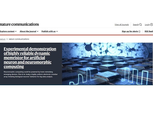
See-On Park, Hakcheon Jeong, Jong-Yong Park - a team of researchers under the leadership of Professor Shinhyun Choi of the School of Electrical Engineering, developed a highly reliable variable resistor (memristor) array that simulates the behavior of neurons using a metal oxide layer with an oxygen concentration gradient, and published their work in Nature Communications. The study was selected as the Nature Communications' Editor's highlight, and as the featured article posted on the main page of the journal's website.
Link : https://www.nature.com/ncomms/
[ Figure 1. The featured image on the main page of the Nature Communications' website introducing the research by Professor Choi's team on the memristor for artificial neurons ]
Thesis title: Experimental demonstration of highly reliable dynamic memristor for artificial neuron and neuromorphic computing.
( https://doi.org/10.1038/s41467-022-30539-6 )
At KAIST, their research was introduced on the 2022 Fall issue of Breakthroughs, the biannual newsletter published by KAIST College of Engineering.
This research was conducted with the support from the Samsung Research Funding & Incubation Center of Samsung Electronics.
2022.11.01 View 10122
Professor Shinhyun Choi’s team, selected for Nature Communications Editors’ highlight
[ From left, Ph.D. candidates See-On Park and Hakcheon Jeong, along with Master's student Jong-Yong Park and Professor Shinhyun Choi ]
See-On Park, Hakcheon Jeong, Jong-Yong Park - a team of researchers under the leadership of Professor Shinhyun Choi of the School of Electrical Engineering, developed a highly reliable variable resistor (memristor) array that simulates the behavior of neurons using a metal oxide layer with an oxygen concentration gradient, and published their work in Nature Communications. The study was selected as the Nature Communications' Editor's highlight, and as the featured article posted on the main page of the journal's website.
Link : https://www.nature.com/ncomms/
[ Figure 1. The featured image on the main page of the Nature Communications' website introducing the research by Professor Choi's team on the memristor for artificial neurons ]
Thesis title: Experimental demonstration of highly reliable dynamic memristor for artificial neuron and neuromorphic computing.
( https://doi.org/10.1038/s41467-022-30539-6 )
At KAIST, their research was introduced on the 2022 Fall issue of Breakthroughs, the biannual newsletter published by KAIST College of Engineering.
This research was conducted with the support from the Samsung Research Funding & Incubation Center of Samsung Electronics.
2022.11.01 View 10122 -
 New Chiral Nanostructures to Extend the Material Platform
Researchers observed a wide window of chiroptical activity from nanomaterials
A research team transferred chirality from the molecular scale to a microscale to extend material platforms and applications. The optical activity from this novel chiral material encompasses to short-wave infrared region.
This platform could serve as a powerful strategy for hierarchical chirality transfer through self-assembly, generating broad optical activity and providing immense applications including bio, telecommunication, and imaging technique. This is the first observation of such a wide window of chiroptical activity from nanomaterials.
“We synthesized chiral copper sulfides using cysteine, as the stabilizer, and transferring the chirality from molecular to the microscale through self-assembly,” explained Professor Jihyeon Yeom from the Department of Materials Science and Engineering, who led the research. The result was reported in ACS Nano on September 14.
Chiral nanomaterials provide a rich platform for versatile applications. Tuning the wavelength of polarization rotation maxima in the broad range is a promising candidate for infrared neural stimulation, imaging, and nanothermometry. However, the majority of previously developed chiral nanomaterials revealed the optical activity in a relatively shorter wavelength range, not in short-wave infrared.
To achieve chiroptical activity in the short-wave infrared region, materials should be in sub-micrometer dimensions, which are compatible with the wavelength of short-wave infrared region light for strong light-matter interaction. They also should have the optical property of short-wave infrared region absorption while forming a structure with chirality.
Professor Yeom’s team induced self-assembly of the chiral nanoparticles by controlling the attraction and repulsion forces between the building block nanoparticles. During this process, molecular chirality of cysteine was transferred to the nanoscale chirality of nanoparticles, and then transferred to the micrometer scale chirality of nanoflowers with 1.5-2 2 μm dimensions formed by the self-assembly.
“We will work to expand the wavelength range of chiroptical activity to the short-wave infrared region, thus reshaping our daily lives in the form of a bio-barcode that can store vast amount of information under the skin,” said Professor Yeom.
This study was funded by the Ministry of Science and ICT, the Ministry of Health and Welfare, the Ministry of Food and Drug Safety, the National Research Foundation of Korea,the KAIST URP Program, the KAIST Creative Challenging Research Program, Samsung and POSCO Science Fellowship.
-PublicationKi Hyun Park, Junyoung Kwon, Uichang Jeong, Ji-Young Kim, Nicholas A.Kotov, Jihyeon Yeom, “Broad Chrioptical Activity from Ultraviolet to Short-Wave Infrared by Chirality Transfer from Molecular to Micrometer Scale," September 14, 2021 ACS Nano (https://doi.org/10.1021/acsnano.1c05888)
-ProfileProfessor Jihyeon YeomNovel Nanomaterials for New Platforms LaboratoryDepartment of Materials Science and EngineeringKAIST
2021.10.22 View 11450
New Chiral Nanostructures to Extend the Material Platform
Researchers observed a wide window of chiroptical activity from nanomaterials
A research team transferred chirality from the molecular scale to a microscale to extend material platforms and applications. The optical activity from this novel chiral material encompasses to short-wave infrared region.
This platform could serve as a powerful strategy for hierarchical chirality transfer through self-assembly, generating broad optical activity and providing immense applications including bio, telecommunication, and imaging technique. This is the first observation of such a wide window of chiroptical activity from nanomaterials.
“We synthesized chiral copper sulfides using cysteine, as the stabilizer, and transferring the chirality from molecular to the microscale through self-assembly,” explained Professor Jihyeon Yeom from the Department of Materials Science and Engineering, who led the research. The result was reported in ACS Nano on September 14.
Chiral nanomaterials provide a rich platform for versatile applications. Tuning the wavelength of polarization rotation maxima in the broad range is a promising candidate for infrared neural stimulation, imaging, and nanothermometry. However, the majority of previously developed chiral nanomaterials revealed the optical activity in a relatively shorter wavelength range, not in short-wave infrared.
To achieve chiroptical activity in the short-wave infrared region, materials should be in sub-micrometer dimensions, which are compatible with the wavelength of short-wave infrared region light for strong light-matter interaction. They also should have the optical property of short-wave infrared region absorption while forming a structure with chirality.
Professor Yeom’s team induced self-assembly of the chiral nanoparticles by controlling the attraction and repulsion forces between the building block nanoparticles. During this process, molecular chirality of cysteine was transferred to the nanoscale chirality of nanoparticles, and then transferred to the micrometer scale chirality of nanoflowers with 1.5-2 2 μm dimensions formed by the self-assembly.
“We will work to expand the wavelength range of chiroptical activity to the short-wave infrared region, thus reshaping our daily lives in the form of a bio-barcode that can store vast amount of information under the skin,” said Professor Yeom.
This study was funded by the Ministry of Science and ICT, the Ministry of Health and Welfare, the Ministry of Food and Drug Safety, the National Research Foundation of Korea,the KAIST URP Program, the KAIST Creative Challenging Research Program, Samsung and POSCO Science Fellowship.
-PublicationKi Hyun Park, Junyoung Kwon, Uichang Jeong, Ji-Young Kim, Nicholas A.Kotov, Jihyeon Yeom, “Broad Chrioptical Activity from Ultraviolet to Short-Wave Infrared by Chirality Transfer from Molecular to Micrometer Scale," September 14, 2021 ACS Nano (https://doi.org/10.1021/acsnano.1c05888)
-ProfileProfessor Jihyeon YeomNovel Nanomaterials for New Platforms LaboratoryDepartment of Materials Science and EngineeringKAIST
2021.10.22 View 11450 -
 Flexible Sensor-Integrated RFA Needle Leads to Smarter Medical Treatment
Clinical trial of flexible sensor-integrated radiofrequency ablation (RFA) needle tip monitors physical changes and steam pop
Researchers have designed a thin polymeric sensor platform on a radiofrequency ablation needle to monitor temperature and pressure in real time. The sensors integrated onto 1.5 mm diameter needle tip have proven their efficacy during clinical tests and expect to provide a new opportunity for safer and more effective medical practices. The research was reported in Advanced Science as the frontispiece on August 5.
Radiofrequency ablation (RFA) is a minimally invasive surgery technique for removing tumors and treating cardiovascular disease. During a procedure, an unintended audible explosion called ‘steam pop’ can occur due to the increased internal steam pressure in the ablation region. This phenomenon has been cited as a cause of various negative thermal and mechanical effects on neighboring tissue. Even more, the relationship between steam pop and cancer recurrence is still being investigated.
Professor Inkyu Park said that his team’s integrated sensors reliably detected the occurrence of steam pop. The sensors also monitor rapidly spreading hot steam in tissue. It is expected that the diverse properties of tissue undergoing RFA could be checked by utilizing the physical sensors integrated on the needle.
“We believe that the integrated sensors can provide useful information about a variety of medical procedures and accompanying environmental changes in the human body, and help develop more effective and safer surgical procedures,” said Professor Park.
Professor Park’s team built a thin film type pressure and temperature sensor stack with a thickness of less than 10 μm using a microfabrication process. For the pressure sensor, the team used contact resistance changes between metal electrodes and a carbon nanotube coated polymeric membrane. The entire sensor array was thoroughly insulated with medical tubes to minimize any exposure of the sensor materials to external tissue and maximize its biocompatibility.
During the clinical trial, the research team found that the accumulated hot steam is suddenly released during steam pops and this hot air spreads to neighboring tissue, which accelerates the ablation process. Furthermore, using in-situ ultrasound imaging and computational simulations, the research team could confirm the non-uniform temperature distribution around the RFA needle can be one of the primary reasons for the steam popping.
Professor Park explained that various physical and chemical sensors for different targets can be added to create other medical devices and industrial tools.
“This result will expand the usability and applicability of current flexible sensor technologies. We are also trying to integrate this sensor onto a 0.3mm diameter needle for in-vivo diagnosis applications and expect that this approach can be applied to other medical treatments as well as the industrial field,” added Professor Park. This study was supported by the National Research Foundation of Korea.
-PublicationJaeho Park, Jinwoo Lee, Hyo Keun Lim, Inkyu Park et al. “Real-Time Internal Steam Pop Detection during Radiofrequency Ablation with a Radiofrequency Ablation Needle Integrated with a Temperature and Pressure Sensor: Preclinical and clinical pilot tests," Advanced Science (https://doi/org/10.1002/advs.202100725) on August 5, 2021
-ProfileProfessor Inkyu ParkMicro & Nano Tranducers Laboratory http://mintlab1.kaist.ac.kr/
Department of Mechanical EngineeringCollege of EngineeringKAIST
2021.10.20 View 9942
Flexible Sensor-Integrated RFA Needle Leads to Smarter Medical Treatment
Clinical trial of flexible sensor-integrated radiofrequency ablation (RFA) needle tip monitors physical changes and steam pop
Researchers have designed a thin polymeric sensor platform on a radiofrequency ablation needle to monitor temperature and pressure in real time. The sensors integrated onto 1.5 mm diameter needle tip have proven their efficacy during clinical tests and expect to provide a new opportunity for safer and more effective medical practices. The research was reported in Advanced Science as the frontispiece on August 5.
Radiofrequency ablation (RFA) is a minimally invasive surgery technique for removing tumors and treating cardiovascular disease. During a procedure, an unintended audible explosion called ‘steam pop’ can occur due to the increased internal steam pressure in the ablation region. This phenomenon has been cited as a cause of various negative thermal and mechanical effects on neighboring tissue. Even more, the relationship between steam pop and cancer recurrence is still being investigated.
Professor Inkyu Park said that his team’s integrated sensors reliably detected the occurrence of steam pop. The sensors also monitor rapidly spreading hot steam in tissue. It is expected that the diverse properties of tissue undergoing RFA could be checked by utilizing the physical sensors integrated on the needle.
“We believe that the integrated sensors can provide useful information about a variety of medical procedures and accompanying environmental changes in the human body, and help develop more effective and safer surgical procedures,” said Professor Park.
Professor Park’s team built a thin film type pressure and temperature sensor stack with a thickness of less than 10 μm using a microfabrication process. For the pressure sensor, the team used contact resistance changes between metal electrodes and a carbon nanotube coated polymeric membrane. The entire sensor array was thoroughly insulated with medical tubes to minimize any exposure of the sensor materials to external tissue and maximize its biocompatibility.
During the clinical trial, the research team found that the accumulated hot steam is suddenly released during steam pops and this hot air spreads to neighboring tissue, which accelerates the ablation process. Furthermore, using in-situ ultrasound imaging and computational simulations, the research team could confirm the non-uniform temperature distribution around the RFA needle can be one of the primary reasons for the steam popping.
Professor Park explained that various physical and chemical sensors for different targets can be added to create other medical devices and industrial tools.
“This result will expand the usability and applicability of current flexible sensor technologies. We are also trying to integrate this sensor onto a 0.3mm diameter needle for in-vivo diagnosis applications and expect that this approach can be applied to other medical treatments as well as the industrial field,” added Professor Park. This study was supported by the National Research Foundation of Korea.
-PublicationJaeho Park, Jinwoo Lee, Hyo Keun Lim, Inkyu Park et al. “Real-Time Internal Steam Pop Detection during Radiofrequency Ablation with a Radiofrequency Ablation Needle Integrated with a Temperature and Pressure Sensor: Preclinical and clinical pilot tests," Advanced Science (https://doi/org/10.1002/advs.202100725) on August 5, 2021
-ProfileProfessor Inkyu ParkMicro & Nano Tranducers Laboratory http://mintlab1.kaist.ac.kr/
Department of Mechanical EngineeringCollege of EngineeringKAIST
2021.10.20 View 9942 -
 Quantum Emitters: Beyond Crystal Clear to Single-Photon Pure
‘Nanoscale Focus Pinspot’ can quench only the background noise without changing the optical properties of the quantum emitter and the built-in photonic structure
Photons, fundamental particles of light, are carrying these words to your eyes via the light from your computer screen or phone. Photons play a key role in the next-generation quantum information technology, such as quantum computing and communications. A quantum emitter, capable of producing a single, pure photon, is the crux of such technology but has many issues that have yet to be solved, according to KAIST researchers.
A research team under Professor Yong-Hoon Cho has developed a technique that can isolate the desired quality emitter by reducing the noise surrounding the target with what they have dubbed a ‘nanoscale focus pinspot.’ They published their results on June 24 in ACS Nano.
“The nanoscale focus pinspot is a structurally nondestructive technique under an extremely low dose ion beam and is generally applicable for various platforms to improve their single-photon purity while retaining the integrated photonic structures,” said lead author Yong-Hoon Cho from the Department of Physics at KAIST.
To produce single photons from solid state materials, the researchers used wide-bandgap semiconductor quantum dots — fabricated nanoparticles with specialized potential properties, such as the ability to directly inject current into a small chip and to operate at room temperature for practical applications. By making a quantum dot in a photonic structure that propagates light, and then irradiating it with helium ions, researchers theorized that they could develop a quantum emitter that could reduce the unwanted noisy background and produce a single, pure photon on demand.
Professor Cho explained, “Despite its high resolution and versatility, a focused ion beam typically suppresses the optical properties around the bombarded area due to the accelerated ion beam’s high momentum. We focused on the fact that, if the focused ion beam is well controlled, only the background noise can be selectively quenched with high spatial resolution without destroying the structure.”
In other words, the researchers focused the ion beam on a mere pin prick, effectively cutting off the interactions around the quantum dot and removing the physical properties that could negatively interact with and degrade the photon purity emitted from the quantum dot.
“It is the first developed technique that can quench the background noise without changing the optical properties of the quantum emitter and the built-in photonic structure,” Professor Cho asserted.
Professor Cho compared it to stimulated emission depletion microscopy, a technique used to decrease the light around the area of focus, but leaving the focal point illuminated. The result is increased resolution of the desired visual target.
“By adjusting the focused ion beam-irradiated region, we can select the target emitter with nanoscale resolution by quenching the surrounding emitter,” Professor Cho said. “This nanoscale selective-quenching technique can be applied to various material and structural platforms and further extended for applications such as optical memory and high-resolution micro displays.” Korea’s National Research Foundation and the Samsung Science and Technology Foundation supported this work.
-PublicationMinho Choi, Seongmoon Jun, and Yong-Hoon Cho et al. ACS Nano‘Nanoscale Focus Pinspot for High-Purity Quantum Emitters via Focused-Ion-Beam-Induced Luminescence Quenching,’(https://pubs.acs.org/doi/10.1021/acsnano.1c00587)
-ProfileProfessor Yong-Hoon ChoQuantum & Nanobio Photonics Laboratoryhttp://qnp.kaist.ac.kr/
Department of PhysicsKAIST
2021.09.02 View 12013
Quantum Emitters: Beyond Crystal Clear to Single-Photon Pure
‘Nanoscale Focus Pinspot’ can quench only the background noise without changing the optical properties of the quantum emitter and the built-in photonic structure
Photons, fundamental particles of light, are carrying these words to your eyes via the light from your computer screen or phone. Photons play a key role in the next-generation quantum information technology, such as quantum computing and communications. A quantum emitter, capable of producing a single, pure photon, is the crux of such technology but has many issues that have yet to be solved, according to KAIST researchers.
A research team under Professor Yong-Hoon Cho has developed a technique that can isolate the desired quality emitter by reducing the noise surrounding the target with what they have dubbed a ‘nanoscale focus pinspot.’ They published their results on June 24 in ACS Nano.
“The nanoscale focus pinspot is a structurally nondestructive technique under an extremely low dose ion beam and is generally applicable for various platforms to improve their single-photon purity while retaining the integrated photonic structures,” said lead author Yong-Hoon Cho from the Department of Physics at KAIST.
To produce single photons from solid state materials, the researchers used wide-bandgap semiconductor quantum dots — fabricated nanoparticles with specialized potential properties, such as the ability to directly inject current into a small chip and to operate at room temperature for practical applications. By making a quantum dot in a photonic structure that propagates light, and then irradiating it with helium ions, researchers theorized that they could develop a quantum emitter that could reduce the unwanted noisy background and produce a single, pure photon on demand.
Professor Cho explained, “Despite its high resolution and versatility, a focused ion beam typically suppresses the optical properties around the bombarded area due to the accelerated ion beam’s high momentum. We focused on the fact that, if the focused ion beam is well controlled, only the background noise can be selectively quenched with high spatial resolution without destroying the structure.”
In other words, the researchers focused the ion beam on a mere pin prick, effectively cutting off the interactions around the quantum dot and removing the physical properties that could negatively interact with and degrade the photon purity emitted from the quantum dot.
“It is the first developed technique that can quench the background noise without changing the optical properties of the quantum emitter and the built-in photonic structure,” Professor Cho asserted.
Professor Cho compared it to stimulated emission depletion microscopy, a technique used to decrease the light around the area of focus, but leaving the focal point illuminated. The result is increased resolution of the desired visual target.
“By adjusting the focused ion beam-irradiated region, we can select the target emitter with nanoscale resolution by quenching the surrounding emitter,” Professor Cho said. “This nanoscale selective-quenching technique can be applied to various material and structural platforms and further extended for applications such as optical memory and high-resolution micro displays.” Korea’s National Research Foundation and the Samsung Science and Technology Foundation supported this work.
-PublicationMinho Choi, Seongmoon Jun, and Yong-Hoon Cho et al. ACS Nano‘Nanoscale Focus Pinspot for High-Purity Quantum Emitters via Focused-Ion-Beam-Induced Luminescence Quenching,’(https://pubs.acs.org/doi/10.1021/acsnano.1c00587)
-ProfileProfessor Yong-Hoon ChoQuantum & Nanobio Photonics Laboratoryhttp://qnp.kaist.ac.kr/
Department of PhysicsKAIST
2021.09.02 View 12013 -
 Brain-Inspired Highly Scalable Neuromorphic Hardware Presented
Neurons and synapses based on single transistor can dramatically reduce the hardware cost and accelerate the commercialization of neuromorphic hardware
KAIST researchers fabricated a brain-inspired highly scalable neuromorphic hardware by co-integrating single transistor neurons and synapses. Using standard silicon complementary metal-oxide-semiconductor (CMOS) technology, the neuromorphic hardware is expected to reduce chip cost and simplify fabrication procedures.
The research team led by Yang-Kyu Choi and Sung-Yool Choi produced a neurons and synapses based on single transistor for highly scalable neuromorphic hardware and showed the ability to recognize text and face images. This research was featured in Science Advances on August 4.
Neuromorphic hardware has attracted a great deal of attention because of its artificial intelligence functions, but consuming ultra-low power of less than 20 watts by mimicking the human brain. To make neuromorphic hardware work, a neuron that generates a spike when integrating a certain signal, and a synapse remembering the connection between two neurons are necessary, just like the biological brain. However, since neurons and synapses constructed on digital or analog circuits occupy a large space, there is a limit in terms of hardware efficiency and costs. Since the human brain consists of about 1011 neurons and 1014 synapses, it is necessary to improve the hardware cost in order to apply it to mobile and IoT devices.
To solve the problem, the research team mimicked the behavior of biological neurons and synapses with a single transistor, and co-integrated them onto an 8-inch wafer. The manufactured neuromorphic transistors have the same structure as the transistors for memory and logic that are currently mass-produced. In addition, the neuromorphic transistors proved for the first time that they can be implemented with a ‘Janus structure’ that functions as both neuron and synapse, just like coins have heads and tails.
Professor Yang-Kyu Choi said that this work can dramatically reduce the hardware cost by replacing the neurons and synapses that were based on complex digital and analog circuits with a single transistor. "We have demonstrated that neurons and synapses can be implemented using a single transistor," said Joon-Kyu Han, the first author. "By co-integrating single transistor neurons and synapses on the same wafer using a standard CMOS process, the hardware cost of the neuromorphic hardware has been improved, which will accelerate the commercialization of neuromorphic hardware,” Han added.This research was supported by the National Research Foundation (NRF) and IC Design Education Center (IDEC).
-PublicationJoon-Kyu Han, Sung-Yool Choi, Yang-Kyu Choi, et al.“Cointegration of single-transistor neurons and synapses by nanoscale CMOS fabrication for highly scalable neuromorphic hardware,” Science Advances (DOI: 10.1126/sciadv.abg8836)
-ProfileProfessor Yang-Kyu ChoiNano-Oriented Bio-Electronics Labhttps://sites.google.com/view/nobelab/
School of Electrical EngineeringKAIST
Professor Sung-Yool ChoiMolecular and Nano Device Laboratoryhttps://www.mndl.kaist.ac.kr/
School of Electrical EngineeringKAIST
2021.08.05 View 12386
Brain-Inspired Highly Scalable Neuromorphic Hardware Presented
Neurons and synapses based on single transistor can dramatically reduce the hardware cost and accelerate the commercialization of neuromorphic hardware
KAIST researchers fabricated a brain-inspired highly scalable neuromorphic hardware by co-integrating single transistor neurons and synapses. Using standard silicon complementary metal-oxide-semiconductor (CMOS) technology, the neuromorphic hardware is expected to reduce chip cost and simplify fabrication procedures.
The research team led by Yang-Kyu Choi and Sung-Yool Choi produced a neurons and synapses based on single transistor for highly scalable neuromorphic hardware and showed the ability to recognize text and face images. This research was featured in Science Advances on August 4.
Neuromorphic hardware has attracted a great deal of attention because of its artificial intelligence functions, but consuming ultra-low power of less than 20 watts by mimicking the human brain. To make neuromorphic hardware work, a neuron that generates a spike when integrating a certain signal, and a synapse remembering the connection between two neurons are necessary, just like the biological brain. However, since neurons and synapses constructed on digital or analog circuits occupy a large space, there is a limit in terms of hardware efficiency and costs. Since the human brain consists of about 1011 neurons and 1014 synapses, it is necessary to improve the hardware cost in order to apply it to mobile and IoT devices.
To solve the problem, the research team mimicked the behavior of biological neurons and synapses with a single transistor, and co-integrated them onto an 8-inch wafer. The manufactured neuromorphic transistors have the same structure as the transistors for memory and logic that are currently mass-produced. In addition, the neuromorphic transistors proved for the first time that they can be implemented with a ‘Janus structure’ that functions as both neuron and synapse, just like coins have heads and tails.
Professor Yang-Kyu Choi said that this work can dramatically reduce the hardware cost by replacing the neurons and synapses that were based on complex digital and analog circuits with a single transistor. "We have demonstrated that neurons and synapses can be implemented using a single transistor," said Joon-Kyu Han, the first author. "By co-integrating single transistor neurons and synapses on the same wafer using a standard CMOS process, the hardware cost of the neuromorphic hardware has been improved, which will accelerate the commercialization of neuromorphic hardware,” Han added.This research was supported by the National Research Foundation (NRF) and IC Design Education Center (IDEC).
-PublicationJoon-Kyu Han, Sung-Yool Choi, Yang-Kyu Choi, et al.“Cointegration of single-transistor neurons and synapses by nanoscale CMOS fabrication for highly scalable neuromorphic hardware,” Science Advances (DOI: 10.1126/sciadv.abg8836)
-ProfileProfessor Yang-Kyu ChoiNano-Oriented Bio-Electronics Labhttps://sites.google.com/view/nobelab/
School of Electrical EngineeringKAIST
Professor Sung-Yool ChoiMolecular and Nano Device Laboratoryhttps://www.mndl.kaist.ac.kr/
School of Electrical EngineeringKAIST
2021.08.05 View 12386 -
 Quantum Laser Turns Energy Loss into Gain
A new laser that generates quantum particles can recycle lost energy for highly efficient, low threshold laser applications
Scientists at KAIST have fabricated a laser system that generates highly interactive quantum particles at room temperature. Their findings, published in the journal Nature Photonics, could lead to a single microcavity laser system that requires lower threshold energy as its energy loss increases.
The system, developed by KAIST physicist Yong-Hoon Cho and colleagues, involves shining light through a single hexagonal-shaped microcavity treated with a loss-modulated silicon nitride substrate. The system design leads to the generation of a polariton laser at room temperature, which is exciting because this usually requires cryogenic temperatures.
The researchers found another unique and counter-intuitive feature of this design. Normally, energy is lost during laser operation. But in this system, as energy loss increased, the amount of energy needed to induce lasing decreased. Exploiting this phenomenon could lead to the development of high efficiency, low threshold lasers for future quantum optical devices.
“This system applies a concept of quantum physics known as parity-time reversal symmetry,” explains Professor Cho. “This is an important platform that allows energy loss to be used as gain. It can be used to reduce laser threshold energy for classical optical devices and sensors, as well as quantum devices and controlling the direction of light.”
The key is the design and materials. The hexagonal microcavity divides light particles into two different modes: one that passes through the upward-facing triangle of the hexagon and another that passes through its downward-facing triangle. Both modes of light particles have the same energy and path but don’t interact with each other.
However, the light particles do interact with other particles called excitons, provided by the hexagonal microcavity, which is made of semiconductors. This interaction leads to the generation of new quantum particles called polaritons that then interact with each other to generate the polariton laser. By controlling the degree of loss between the microcavity and the semiconductor substrate, an intriguing phenomenon arises, with the threshold energy becoming smaller as energy loss increases. This research was supported by the Samsung Science and Technology Foundation and Korea’s National Research Foundation.
-PublicationSong,H.G, Choi, M, Woo, K.Y. Yong-Hoon Cho Room-temperature polaritonic non-Hermitian system with single microcavityNature Photonics (https://doi.org/10.1038/s41566-021-00820-z)
-ProfileProfessor Yong-Hoon ChoQuantum & Nanobio Photonics Laboratoryhttp://qnp.kaist.ac.kr/
Department of PhysicsKAIST
2021.07.07 View 11554
Quantum Laser Turns Energy Loss into Gain
A new laser that generates quantum particles can recycle lost energy for highly efficient, low threshold laser applications
Scientists at KAIST have fabricated a laser system that generates highly interactive quantum particles at room temperature. Their findings, published in the journal Nature Photonics, could lead to a single microcavity laser system that requires lower threshold energy as its energy loss increases.
The system, developed by KAIST physicist Yong-Hoon Cho and colleagues, involves shining light through a single hexagonal-shaped microcavity treated with a loss-modulated silicon nitride substrate. The system design leads to the generation of a polariton laser at room temperature, which is exciting because this usually requires cryogenic temperatures.
The researchers found another unique and counter-intuitive feature of this design. Normally, energy is lost during laser operation. But in this system, as energy loss increased, the amount of energy needed to induce lasing decreased. Exploiting this phenomenon could lead to the development of high efficiency, low threshold lasers for future quantum optical devices.
“This system applies a concept of quantum physics known as parity-time reversal symmetry,” explains Professor Cho. “This is an important platform that allows energy loss to be used as gain. It can be used to reduce laser threshold energy for classical optical devices and sensors, as well as quantum devices and controlling the direction of light.”
The key is the design and materials. The hexagonal microcavity divides light particles into two different modes: one that passes through the upward-facing triangle of the hexagon and another that passes through its downward-facing triangle. Both modes of light particles have the same energy and path but don’t interact with each other.
However, the light particles do interact with other particles called excitons, provided by the hexagonal microcavity, which is made of semiconductors. This interaction leads to the generation of new quantum particles called polaritons that then interact with each other to generate the polariton laser. By controlling the degree of loss between the microcavity and the semiconductor substrate, an intriguing phenomenon arises, with the threshold energy becoming smaller as energy loss increases. This research was supported by the Samsung Science and Technology Foundation and Korea’s National Research Foundation.
-PublicationSong,H.G, Choi, M, Woo, K.Y. Yong-Hoon Cho Room-temperature polaritonic non-Hermitian system with single microcavityNature Photonics (https://doi.org/10.1038/s41566-021-00820-z)
-ProfileProfessor Yong-Hoon ChoQuantum & Nanobio Photonics Laboratoryhttp://qnp.kaist.ac.kr/
Department of PhysicsKAIST
2021.07.07 View 11554