Micro
-
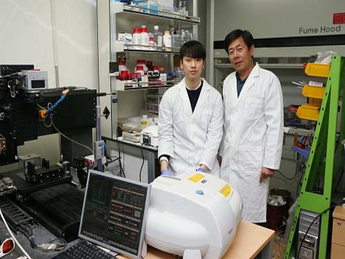 Easier Way to Produce High Performing, Flexible Micro-Supercapacitor
(Professor Minyang Yang and PhD Student Jae Hak Lee)
Professor Minyang Yang from the Department of Mechanical Engineering and his team developed a high-energy, flexible micro-supercapacitor in a simple and cost-effective way.
Compared to conventional micro-batteries, such as lithium-ion batteries, these new batteries, also called supercapacitors, are significantly faster to charge and semi-permanent.
Thin, flexible micro-supercapacitors can be a power source directly attached to wearable and flexible electronics.
However, fabrication of these micro-supercapacitors requires a complex patterning process, such as lithography techniques and vacuum evaporation. Hence, the process requires expensive instruments and toxic chemicals.
To simplify the fabrication of micro-supercapacitors in an eco-friendly manner, the team developed laser growth sintering technology. This technology manufactures superporous silver electrodes and applies them to the supercapacitors’ electrodes.
The team used a laser to form micro-patterns and generated nanoporous structures inside. This laser-induced growth sintering contributed to shortening the manufacturing process from ten steps to one.
Moreover, the team explored this unique laser growth sintering process –nucleation, growth, and sintering –by employing a particle-free, organometallic solution, which is not costly compared to typical laser-sintering methods for metallic nanoparticle solutions used in the printing of micro-electrodes.
Finally, unlike the typical supercapacitors comprised of a single substance, the team applied an asymmetric electrode configuration of nanoporous gold and manganese dioxide, which exhibits a highly-specific capacitance, to operate at a high voltage.
This method allows the team to develop energy storage with a high capacity. This developed micro-supercapacitor only requires four seconds to be charged and passed more than 5,000 durability tests.
Professor Yang said, “This research outcome can be used as energy storage installed in wearable and flexible electronic devices. Through this research, we are one step closer to realizing a complete version of flexible electronic devices by incorporating a power supply.”
This research, led by PhD candidate Jae Hak Lee, was selected as the cover of Journal of Materials Chemistry A on December 21, 2017.
Figure 1. Cover of the Journal Materials Chemistry A
Figure 2. Manufactured micro-supercapacitor and its performance
Figure 3. Laser growth sintering mechanism
Figure 4. Structural change of the silver conductor according to the irradiated laser energy
2018.01.18 View 8201
Easier Way to Produce High Performing, Flexible Micro-Supercapacitor
(Professor Minyang Yang and PhD Student Jae Hak Lee)
Professor Minyang Yang from the Department of Mechanical Engineering and his team developed a high-energy, flexible micro-supercapacitor in a simple and cost-effective way.
Compared to conventional micro-batteries, such as lithium-ion batteries, these new batteries, also called supercapacitors, are significantly faster to charge and semi-permanent.
Thin, flexible micro-supercapacitors can be a power source directly attached to wearable and flexible electronics.
However, fabrication of these micro-supercapacitors requires a complex patterning process, such as lithography techniques and vacuum evaporation. Hence, the process requires expensive instruments and toxic chemicals.
To simplify the fabrication of micro-supercapacitors in an eco-friendly manner, the team developed laser growth sintering technology. This technology manufactures superporous silver electrodes and applies them to the supercapacitors’ electrodes.
The team used a laser to form micro-patterns and generated nanoporous structures inside. This laser-induced growth sintering contributed to shortening the manufacturing process from ten steps to one.
Moreover, the team explored this unique laser growth sintering process –nucleation, growth, and sintering –by employing a particle-free, organometallic solution, which is not costly compared to typical laser-sintering methods for metallic nanoparticle solutions used in the printing of micro-electrodes.
Finally, unlike the typical supercapacitors comprised of a single substance, the team applied an asymmetric electrode configuration of nanoporous gold and manganese dioxide, which exhibits a highly-specific capacitance, to operate at a high voltage.
This method allows the team to develop energy storage with a high capacity. This developed micro-supercapacitor only requires four seconds to be charged and passed more than 5,000 durability tests.
Professor Yang said, “This research outcome can be used as energy storage installed in wearable and flexible electronic devices. Through this research, we are one step closer to realizing a complete version of flexible electronic devices by incorporating a power supply.”
This research, led by PhD candidate Jae Hak Lee, was selected as the cover of Journal of Materials Chemistry A on December 21, 2017.
Figure 1. Cover of the Journal Materials Chemistry A
Figure 2. Manufactured micro-supercapacitor and its performance
Figure 3. Laser growth sintering mechanism
Figure 4. Structural change of the silver conductor according to the irradiated laser energy
2018.01.18 View 8201 -
 Novel Photolithographic Technology Enabling 3D Control over Functional Shapes of Microstructures
Professor Shin-Hyun Kim and his research team in the Department of Chemical and Biomolecular Engineering at KAIST have developed a novel photolithographic technology enabling control over the functional shapes of micropatterns using oxygen diffusion.
The research was published online in the March 13th issue of Nature Communications and was selected as a featured image for the journal.
Photolithography is a standard optical process for transferring micropatterns on to a substrate by exposing specific regions of the photoresist layer to ultraviolet (UV) light. It is used widely throughout industries that require micropatterns, especially in the semiconductor manufacturing industry.
Conventional photolithography relied on photomasks which protected certain regions of the substrate from the input UV light. Areas covered by the photomasks remain intact with the base layer while the areas exposed to the UV light are washed away, thus creating a micropattern. This technology was limited to a two-dimensional, disc-shaped design as the boundaries between the exposed and roofed regions are always in a parallel arrangement with the direction of the light.
Professor Kim’s research team discovered that: 1) the areas exposed to UV light lowered the concentration of oxygen and thus resulted in oxygen diffusion; and 2) manipulation of the diffusion speed and direction allowed control of the growth, shape and size of the polymers. Based on these findings, the team developed a new photolithographic technology that enabled the production of micropatterns with three-dimensional structures in various shapes and sizes.
Oxygen was considered an inhibitor during photopolymerization. Photoresist under UV light creates radicals which initialize a chemical reaction. These radicals are eliminated with the presence of oxygen and thus prevents the reaction. This suggests that the photoresist must be exposed to UV light for an extended time to completely remove oxygen for a chemical reaction to begin.
The research team, however, exploited the presence of oxygen. While the region affected by the UV light lowered oxygen concentration, the concentration in the untouched region remained unchanged. This difference in the concentrations caused a diffusion of oxygen to the region under UV light.
When the speed of the oxygen flow is slow, the diffusion occurs in parallel with the direction of the UV light. When fast, the diffusion process develops horizontally, outward from the area affected by the UV light. Professor Kim and his team proved this phenomenon both empirically and theoretically. Furthermore, by injecting an external oxygen source, the team was able to manipulate diffusion strength and direction, and thus control the shape and size of the polymer. The use of the polymerization inhibitors enabled and facilitated the fabrication of complex, three-dimensional micropatterns.
Professor Kim said, “While 3D printing is considered an innovative manufacturing technology, it cannot be used for mass-production of microscopic products. The new photolithographic technology will have a broad impact on both the academia and industry especially because existing, conventional photolithographic equipment can be used for the development of more complex micropatterns.” His newest technology will enhance the manufacturing process of three-dimensional polymers which were considered difficult to be commercialized.
The research was also dedicated to the late Professor Seung-Man Yang of the Department of Chemical and Biomolecular Engineering at KAIST. He was considered one of the greatest scholars in Korea in the field of hydrodynamics and colloids.
Picture 1: Featured Image of Nature Communications, March 2015
Picture 2: Polymers with various shapes and sizes produced with the new photolithographic technology developed by Professor Kim
2015.04.06 View 11064
Novel Photolithographic Technology Enabling 3D Control over Functional Shapes of Microstructures
Professor Shin-Hyun Kim and his research team in the Department of Chemical and Biomolecular Engineering at KAIST have developed a novel photolithographic technology enabling control over the functional shapes of micropatterns using oxygen diffusion.
The research was published online in the March 13th issue of Nature Communications and was selected as a featured image for the journal.
Photolithography is a standard optical process for transferring micropatterns on to a substrate by exposing specific regions of the photoresist layer to ultraviolet (UV) light. It is used widely throughout industries that require micropatterns, especially in the semiconductor manufacturing industry.
Conventional photolithography relied on photomasks which protected certain regions of the substrate from the input UV light. Areas covered by the photomasks remain intact with the base layer while the areas exposed to the UV light are washed away, thus creating a micropattern. This technology was limited to a two-dimensional, disc-shaped design as the boundaries between the exposed and roofed regions are always in a parallel arrangement with the direction of the light.
Professor Kim’s research team discovered that: 1) the areas exposed to UV light lowered the concentration of oxygen and thus resulted in oxygen diffusion; and 2) manipulation of the diffusion speed and direction allowed control of the growth, shape and size of the polymers. Based on these findings, the team developed a new photolithographic technology that enabled the production of micropatterns with three-dimensional structures in various shapes and sizes.
Oxygen was considered an inhibitor during photopolymerization. Photoresist under UV light creates radicals which initialize a chemical reaction. These radicals are eliminated with the presence of oxygen and thus prevents the reaction. This suggests that the photoresist must be exposed to UV light for an extended time to completely remove oxygen for a chemical reaction to begin.
The research team, however, exploited the presence of oxygen. While the region affected by the UV light lowered oxygen concentration, the concentration in the untouched region remained unchanged. This difference in the concentrations caused a diffusion of oxygen to the region under UV light.
When the speed of the oxygen flow is slow, the diffusion occurs in parallel with the direction of the UV light. When fast, the diffusion process develops horizontally, outward from the area affected by the UV light. Professor Kim and his team proved this phenomenon both empirically and theoretically. Furthermore, by injecting an external oxygen source, the team was able to manipulate diffusion strength and direction, and thus control the shape and size of the polymer. The use of the polymerization inhibitors enabled and facilitated the fabrication of complex, three-dimensional micropatterns.
Professor Kim said, “While 3D printing is considered an innovative manufacturing technology, it cannot be used for mass-production of microscopic products. The new photolithographic technology will have a broad impact on both the academia and industry especially because existing, conventional photolithographic equipment can be used for the development of more complex micropatterns.” His newest technology will enhance the manufacturing process of three-dimensional polymers which were considered difficult to be commercialized.
The research was also dedicated to the late Professor Seung-Man Yang of the Department of Chemical and Biomolecular Engineering at KAIST. He was considered one of the greatest scholars in Korea in the field of hydrodynamics and colloids.
Picture 1: Featured Image of Nature Communications, March 2015
Picture 2: Polymers with various shapes and sizes produced with the new photolithographic technology developed by Professor Kim
2015.04.06 View 11064 -
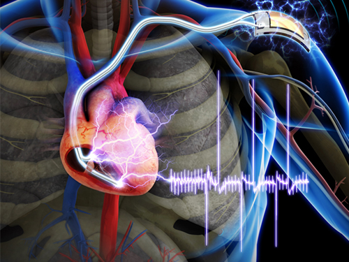 The First Demonstration of a Self-powered Cardiac Pacemaker
As the number of pacemakers implanted each year reaches into the millions worldwide, improving the lifespan of pacemaker batteries has been of great concern for developers and manufacturers. Currently, pacemaker batteries last seven years on average, requiring frequent replacements, which may pose patients to a potential risk involved in medical procedures.
A research team from the Korea Advanced Institute of Science and Technology (KAIST), headed by Professor Keon Jae Lee of the Department of Materials Science and Engineering at KAIST and Professor Boyoung Joung, M.D. of the Division of Cardiology at Severance Hospital of Yonsei University, has developed a self-powered artificial cardiac pacemaker that is operated semi-permanently by a flexible piezoelectric nanogenerator.
The artificial cardiac pacemaker is widely acknowledged as medical equipment that is integrated into the human body to regulate the heartbeats through electrical stimulation to contract the cardiac muscles of people who suffer from arrhythmia. However, repeated surgeries to replace pacemaker batteries have exposed elderly patients to health risks such as infections or severe bleeding during operations.
The team’s newly designed flexible piezoelectric nanogenerator directly stimulated a living rat’s heart using electrical energy converted from the small body movements of the rat. This technology could facilitate the use of self-powered flexible energy harvesters, not only prolonging the lifetime of cardiac pacemakers but also realizing real-time heart monitoring.
The research team fabricated high-performance flexible nanogenerators utilizing a bulk single-crystal PMN-PT thin film (iBULe Photonics). The harvested energy reached up to 8.2 V and 0.22 mA by bending and pushing motions, which were high enough values to directly stimulate the rat’s heart.
Professor Keon Jae Lee said:
“For clinical purposes, the current achievement will benefit the development of self-powered cardiac pacemakers as well as prevent heart attacks via the real-time diagnosis of heart arrhythmia. In addition, the flexible piezoelectric nanogenerator could also be utilized as an electrical source for various implantable medical devices.”
This research result was described in the April online issue of Advanced Materials (“Self-Powered Cardiac Pacemaker Enabled by Flexible Single Crystalline PMN-PT Piezoelectric Energy Harvester”: http://onlinelibrary.wiley.com/doi/10.1002/adma.201400562/abstract).
Youtube link: http://www.youtube.com/watch?v=ZWYT2cU_Mog&feature=youtu.be
Picture Caption: A self-powered cardiac pacemaker is enabled by a flexible piezoelectric energy harvester.
2014.06.25 View 17459
The First Demonstration of a Self-powered Cardiac Pacemaker
As the number of pacemakers implanted each year reaches into the millions worldwide, improving the lifespan of pacemaker batteries has been of great concern for developers and manufacturers. Currently, pacemaker batteries last seven years on average, requiring frequent replacements, which may pose patients to a potential risk involved in medical procedures.
A research team from the Korea Advanced Institute of Science and Technology (KAIST), headed by Professor Keon Jae Lee of the Department of Materials Science and Engineering at KAIST and Professor Boyoung Joung, M.D. of the Division of Cardiology at Severance Hospital of Yonsei University, has developed a self-powered artificial cardiac pacemaker that is operated semi-permanently by a flexible piezoelectric nanogenerator.
The artificial cardiac pacemaker is widely acknowledged as medical equipment that is integrated into the human body to regulate the heartbeats through electrical stimulation to contract the cardiac muscles of people who suffer from arrhythmia. However, repeated surgeries to replace pacemaker batteries have exposed elderly patients to health risks such as infections or severe bleeding during operations.
The team’s newly designed flexible piezoelectric nanogenerator directly stimulated a living rat’s heart using electrical energy converted from the small body movements of the rat. This technology could facilitate the use of self-powered flexible energy harvesters, not only prolonging the lifetime of cardiac pacemakers but also realizing real-time heart monitoring.
The research team fabricated high-performance flexible nanogenerators utilizing a bulk single-crystal PMN-PT thin film (iBULe Photonics). The harvested energy reached up to 8.2 V and 0.22 mA by bending and pushing motions, which were high enough values to directly stimulate the rat’s heart.
Professor Keon Jae Lee said:
“For clinical purposes, the current achievement will benefit the development of self-powered cardiac pacemakers as well as prevent heart attacks via the real-time diagnosis of heart arrhythmia. In addition, the flexible piezoelectric nanogenerator could also be utilized as an electrical source for various implantable medical devices.”
This research result was described in the April online issue of Advanced Materials (“Self-Powered Cardiac Pacemaker Enabled by Flexible Single Crystalline PMN-PT Piezoelectric Energy Harvester”: http://onlinelibrary.wiley.com/doi/10.1002/adma.201400562/abstract).
Youtube link: http://www.youtube.com/watch?v=ZWYT2cU_Mog&feature=youtu.be
Picture Caption: A self-powered cardiac pacemaker is enabled by a flexible piezoelectric energy harvester.
2014.06.25 View 17459 -
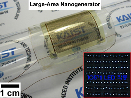 KAIST Made Great Improvements of Nanogenerator Power Efficiency
The energy efficiency of a piezoelectric nanogenerator developed by KAIST has increased by almost 40 times, one step closer toward the commercialization of flexible energy harvesters that can supply power infinitely to wearable, implantable electronic devices.
NANOGENERATORS are innovative self-powered energy harvesters that convert kinetic energy created from vibrational and mechanical sources into electrical power, removing the need of external circuits or batteries for electronic devices. This innovation is vital in realizing sustainable energy generation in isolated, inaccessible, or indoor environments and even in the human body.
Nanogenerators, a flexible and lightweight energy harvester on a plastic substrate, can scavenge energy from the extremely tiny movements of natural resources and human body such as wind, water flow, heartbeats, and diaphragm and respiration activities to generate electrical signals. The generators are not only self-powered, flexible devices but also can provide permanent power sources to implantable biomedical devices, including cardiac pacemakers and deep brain stimulators.
However, poor energy efficiency and a complex fabrication process have posed challenges to the commercialization of nanogenerators. Keon Jae Lee, Associate Professor of Materials Science and Engineering at KAIST, and his colleagues have recently proposed a solution by developing a robust technique to transfer a high-quality piezoelectric thin film from bulk sapphire substrates to plastic substrates using laser lift-off (LLO).
Applying the inorganic-based laser lift-off (LLO) process, the research team produced a large-area PZT thin film nanogenerators on flexible substrates (2cm x 2cm).
“We were able to convert a high-output performance of ~250 V from the slight mechanical deformation of a single thin plastic substrate. Such output power is just enough to turn on 100 LED lights,” Keon Jae Lee explained.
The self-powered nanogenerators can also work with finger and foot motions. For example, under the irregular and slight bending motions of a human finger, the measured current signals had a high electric power of ~8.7 μA. In addition, the piezoelectric nanogenerator has world-record power conversion efficiency, almost 40 times higher than previously reported similar research results, solving the drawbacks related to the fabrication complexity and low energy efficiency.
Lee further commented,
“Building on this concept, it is highly expected that tiny mechanical motions, including human body movements of muscle contraction and relaxation, can be readily converted into electrical energy and, furthermore, acted as eternal power sources.”
The research team is currently studying a method to build three-dimensional stacking of flexible piezoelectric thin films to enhance output power, as well as conducting a clinical experiment with a flexible nanogenerator.
This research result, entitled “Highly-efficient, Flexible Piezoelectric PZT Thin Film Nanogenerator on Plastic Substrates,” was published as the cover article of the April issue of Advanced Materials. (http://onlinelibrary.wiley.com/doi/10.1002/adma.201305659/abstract)
YouTube Link: http://www.youtube.com/watch?v=G_Fny7Xb9ig
Over 100 LEDs operated by self-powered flexible piezoelectric thin film nanogenerator
Flexible PZT thin film nanogenerator using inorganic-based laser lift-off process
Photograph of large-area PZT thin film nanogenerator (3.5cm × 3.5cm) on a curved glass tube and 105 commercial LEDs operated by self-powered flexible piezoelectric energy harvester
2014.05.19 View 15228
KAIST Made Great Improvements of Nanogenerator Power Efficiency
The energy efficiency of a piezoelectric nanogenerator developed by KAIST has increased by almost 40 times, one step closer toward the commercialization of flexible energy harvesters that can supply power infinitely to wearable, implantable electronic devices.
NANOGENERATORS are innovative self-powered energy harvesters that convert kinetic energy created from vibrational and mechanical sources into electrical power, removing the need of external circuits or batteries for electronic devices. This innovation is vital in realizing sustainable energy generation in isolated, inaccessible, or indoor environments and even in the human body.
Nanogenerators, a flexible and lightweight energy harvester on a plastic substrate, can scavenge energy from the extremely tiny movements of natural resources and human body such as wind, water flow, heartbeats, and diaphragm and respiration activities to generate electrical signals. The generators are not only self-powered, flexible devices but also can provide permanent power sources to implantable biomedical devices, including cardiac pacemakers and deep brain stimulators.
However, poor energy efficiency and a complex fabrication process have posed challenges to the commercialization of nanogenerators. Keon Jae Lee, Associate Professor of Materials Science and Engineering at KAIST, and his colleagues have recently proposed a solution by developing a robust technique to transfer a high-quality piezoelectric thin film from bulk sapphire substrates to plastic substrates using laser lift-off (LLO).
Applying the inorganic-based laser lift-off (LLO) process, the research team produced a large-area PZT thin film nanogenerators on flexible substrates (2cm x 2cm).
“We were able to convert a high-output performance of ~250 V from the slight mechanical deformation of a single thin plastic substrate. Such output power is just enough to turn on 100 LED lights,” Keon Jae Lee explained.
The self-powered nanogenerators can also work with finger and foot motions. For example, under the irregular and slight bending motions of a human finger, the measured current signals had a high electric power of ~8.7 μA. In addition, the piezoelectric nanogenerator has world-record power conversion efficiency, almost 40 times higher than previously reported similar research results, solving the drawbacks related to the fabrication complexity and low energy efficiency.
Lee further commented,
“Building on this concept, it is highly expected that tiny mechanical motions, including human body movements of muscle contraction and relaxation, can be readily converted into electrical energy and, furthermore, acted as eternal power sources.”
The research team is currently studying a method to build three-dimensional stacking of flexible piezoelectric thin films to enhance output power, as well as conducting a clinical experiment with a flexible nanogenerator.
This research result, entitled “Highly-efficient, Flexible Piezoelectric PZT Thin Film Nanogenerator on Plastic Substrates,” was published as the cover article of the April issue of Advanced Materials. (http://onlinelibrary.wiley.com/doi/10.1002/adma.201305659/abstract)
YouTube Link: http://www.youtube.com/watch?v=G_Fny7Xb9ig
Over 100 LEDs operated by self-powered flexible piezoelectric thin film nanogenerator
Flexible PZT thin film nanogenerator using inorganic-based laser lift-off process
Photograph of large-area PZT thin film nanogenerator (3.5cm × 3.5cm) on a curved glass tube and 105 commercial LEDs operated by self-powered flexible piezoelectric energy harvester
2014.05.19 View 15228 -
 Immune Evasion Mechanism of Hepatitis C Virus Revealed
Professor Ui-Cheol Shin
Inhibiting major histocompatibility complex [MHC] class I protein expression, T cell immune response is evaded.
The research will be a great help to the development of C hepatitis vaccine.
Roughly 1-2% of the population in Korea is known to be infected with Hepatitis C. Most Hepatitis C Virus (HCV) infections progress to a chronic disease and can cause liver cirrhosis or liver cancer, which may lead to death.
Unlike Hepatitis type A or B, there is no vaccine for Hepatitis C Virus and therefore avoiding exposure to the virus is the best known method of prevention. However, a team of researchers at KAIST has produced research results, which may contribute significantly to the vaccine development.
KAIST Graduate School of Medical Sciences & Engineering’ Professor Ui-Cheol Shin and his team have successfully identified why Hepatitis C Virus does not cause an immune response within the human body. The research results were published in the May edition of The Journal of Gastroenterology, a world-renowned journal in the field of gastroenterology.
The immune response occurs to eliminate the virus that has invaded our body. During this process, a major histocompatibility complex [MHC] class I plays a key role in inducing T cell response, which is needed for the elimination of virus-infected cells.
When a cell is infected by a virus, a substance called interferon causes the increased expression of major histocompatibility complex class I. T cell recognizes the increased MHC class I and therefore finds the virus-infected cells.
However, the effect that Hepatitis C Virus has on major histocompatibility complex class I has not been clearly identified until now.
The research team has revealed, using a cell culture for infection systems, that the Hepatitis C Virus suppresses the expression of major histocompatibility complex class I. Also, the mechanism to prove that HCV activates a protein called PKR within the cell to inhibit MHC class I protein expression was identified at a molecular level.
In this study, researchers established the hypothesis that regulating PKR protein in the cell can enhance the T cell immune response, which was then proved through experiments.
Professor Ui-Cheol Shin said, “There are a lot of new drugs to treat Hepatitis C Virus, while its vaccine has not been developed yet. Revealing the HCV immune evasion mechanism will help stimulate momentum for the HCV vaccine development.”
The first author of the journal, Dr. Won-Seok Kang is a graduate from Yonsei College of Medicine. After earning his medical degree, he has continued his training as a ‘doctor-scientist’ at KAIST Graduate School of Medical Sciences & Engineering to study Hepatitis C Virus immune evasion mechanism in this research.
Hepatitis C Virus activates PKR-eIF2a pathway, which inhibits the major histocompatibility complex class I, and therefore weakens the T cell activation to the viral activity.
2014.05.19 View 11514
Immune Evasion Mechanism of Hepatitis C Virus Revealed
Professor Ui-Cheol Shin
Inhibiting major histocompatibility complex [MHC] class I protein expression, T cell immune response is evaded.
The research will be a great help to the development of C hepatitis vaccine.
Roughly 1-2% of the population in Korea is known to be infected with Hepatitis C. Most Hepatitis C Virus (HCV) infections progress to a chronic disease and can cause liver cirrhosis or liver cancer, which may lead to death.
Unlike Hepatitis type A or B, there is no vaccine for Hepatitis C Virus and therefore avoiding exposure to the virus is the best known method of prevention. However, a team of researchers at KAIST has produced research results, which may contribute significantly to the vaccine development.
KAIST Graduate School of Medical Sciences & Engineering’ Professor Ui-Cheol Shin and his team have successfully identified why Hepatitis C Virus does not cause an immune response within the human body. The research results were published in the May edition of The Journal of Gastroenterology, a world-renowned journal in the field of gastroenterology.
The immune response occurs to eliminate the virus that has invaded our body. During this process, a major histocompatibility complex [MHC] class I plays a key role in inducing T cell response, which is needed for the elimination of virus-infected cells.
When a cell is infected by a virus, a substance called interferon causes the increased expression of major histocompatibility complex class I. T cell recognizes the increased MHC class I and therefore finds the virus-infected cells.
However, the effect that Hepatitis C Virus has on major histocompatibility complex class I has not been clearly identified until now.
The research team has revealed, using a cell culture for infection systems, that the Hepatitis C Virus suppresses the expression of major histocompatibility complex class I. Also, the mechanism to prove that HCV activates a protein called PKR within the cell to inhibit MHC class I protein expression was identified at a molecular level.
In this study, researchers established the hypothesis that regulating PKR protein in the cell can enhance the T cell immune response, which was then proved through experiments.
Professor Ui-Cheol Shin said, “There are a lot of new drugs to treat Hepatitis C Virus, while its vaccine has not been developed yet. Revealing the HCV immune evasion mechanism will help stimulate momentum for the HCV vaccine development.”
The first author of the journal, Dr. Won-Seok Kang is a graduate from Yonsei College of Medicine. After earning his medical degree, he has continued his training as a ‘doctor-scientist’ at KAIST Graduate School of Medical Sciences & Engineering to study Hepatitis C Virus immune evasion mechanism in this research.
Hepatitis C Virus activates PKR-eIF2a pathway, which inhibits the major histocompatibility complex class I, and therefore weakens the T cell activation to the viral activity.
2014.05.19 View 11514 -
 Mechanism in regulation of cancer-related key enzyme, ATM, for DNA damage and repair revealed
Professor Kwang-Wook Choi
A research team led by Professor Kwang-Wook Choi and Dr. Seong-Tae Hong from the Department of Biological Sciences at KAIST has successfully investigated the operational mechanism of the protein Ataxia Telangiectasia Mutated (ATM), an essential protein to the function of a crucial key enzyme that repairs the damaged DNA which stores biometric information. The results were published on December 19th Nature Communications online edition.
All organisms, including humans, constantly strive to protect the information within their DNA from damages posed by a number of factors, such as carbonized materials in our daily food intake, radioactive materials such as radon emitting from the cement of buildings or ultraviolet of the sunlight, which could be a trigger for cancer.
In order to keep the DNA information safe, the organisms are always carrying out complex and sophisticated DNA repair work, which involves the crucial DNA damage repair protein ATM. Consequently, a faulty ATM leads to higher risks of cancer.
Until now, academia predicted that the Translationally Controlled Tumor Protein (TCTP) will play an important role in regulating the function of ATM. However, since most of main research regarding TCTP has only been conducted in cultured cells, it was unable to identify exactly what mechanisms TCTP employs to control ATM.
The KAIST research team identified that TCTP can combine with ATM or increase the enzymatic activity of ATM. In addition, Drosophilia, one of the most widely used model organisms for molecular genetics, has been used to identify that TCTP and ATM play a very important role in repairing the DNA damaged by radiation. This information has allowed the researchers to establish TCTP’s essential function in maintaining the DNA information in cell cultures and even in higher organisms, and to provide specific and important clues to the regulation of ATM by TCTP.
Professor Kwang-Wook Choi said, “Our research is a good example that basic research using Drosophilia can make important contributions to understanding the process of diseases, such as cancer, and to developing adequate treatment.”
The research has been funded by the Ministry of Science, ICT and Future Planning, Republic of Korea, and the National Research Foundation of Korea.
Figure 1. When the amount of TCTP protein is reduced, cells of the Drosophila's eye are abnormally deformed by radiation. Scale bars = 200mm
Figure 2. When the amount of TCTP protein is reduced, the chromosomes of Drosophilia are easily broken by radiation. Scale bars = 10 mm.
Figure 3. When gene expressions of TCTP and ATM are reduced, large defects occur in the normal development of the eye. (Left: normal Drosophilia's eye, right: development-deficient eye)
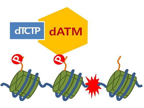
Figure 4. ATM marks the position of the broken DNA, with TCTP helping to facilitate this reaction. DNA (blue line) within the cell nucleus is coiled around the histone protein (green cylinder). When DNA is broken, ATM protein attaches a phosphate group (P). Multiple DNA repair protein recognizes the phosphate as a signal that requires repair and gathers at the site.
2014.01.07 View 14329
Mechanism in regulation of cancer-related key enzyme, ATM, for DNA damage and repair revealed
Professor Kwang-Wook Choi
A research team led by Professor Kwang-Wook Choi and Dr. Seong-Tae Hong from the Department of Biological Sciences at KAIST has successfully investigated the operational mechanism of the protein Ataxia Telangiectasia Mutated (ATM), an essential protein to the function of a crucial key enzyme that repairs the damaged DNA which stores biometric information. The results were published on December 19th Nature Communications online edition.
All organisms, including humans, constantly strive to protect the information within their DNA from damages posed by a number of factors, such as carbonized materials in our daily food intake, radioactive materials such as radon emitting from the cement of buildings or ultraviolet of the sunlight, which could be a trigger for cancer.
In order to keep the DNA information safe, the organisms are always carrying out complex and sophisticated DNA repair work, which involves the crucial DNA damage repair protein ATM. Consequently, a faulty ATM leads to higher risks of cancer.
Until now, academia predicted that the Translationally Controlled Tumor Protein (TCTP) will play an important role in regulating the function of ATM. However, since most of main research regarding TCTP has only been conducted in cultured cells, it was unable to identify exactly what mechanisms TCTP employs to control ATM.
The KAIST research team identified that TCTP can combine with ATM or increase the enzymatic activity of ATM. In addition, Drosophilia, one of the most widely used model organisms for molecular genetics, has been used to identify that TCTP and ATM play a very important role in repairing the DNA damaged by radiation. This information has allowed the researchers to establish TCTP’s essential function in maintaining the DNA information in cell cultures and even in higher organisms, and to provide specific and important clues to the regulation of ATM by TCTP.
Professor Kwang-Wook Choi said, “Our research is a good example that basic research using Drosophilia can make important contributions to understanding the process of diseases, such as cancer, and to developing adequate treatment.”
The research has been funded by the Ministry of Science, ICT and Future Planning, Republic of Korea, and the National Research Foundation of Korea.
Figure 1. When the amount of TCTP protein is reduced, cells of the Drosophila's eye are abnormally deformed by radiation. Scale bars = 200mm
Figure 2. When the amount of TCTP protein is reduced, the chromosomes of Drosophilia are easily broken by radiation. Scale bars = 10 mm.
Figure 3. When gene expressions of TCTP and ATM are reduced, large defects occur in the normal development of the eye. (Left: normal Drosophilia's eye, right: development-deficient eye)
Figure 4. ATM marks the position of the broken DNA, with TCTP helping to facilitate this reaction. DNA (blue line) within the cell nucleus is coiled around the histone protein (green cylinder). When DNA is broken, ATM protein attaches a phosphate group (P). Multiple DNA repair protein recognizes the phosphate as a signal that requires repair and gathers at the site.
2014.01.07 View 14329 -
 Nanowire Made of Diverse Materials May Become Marketable
- Technology to commercialize nanowire developed after 2 years of industrial-academic joint research -
- 2 million strands of 50nm-width, 20 cm-length nanowire mass producible in 2 hours –
A South Korean joint industrial-academic research team has developed the technology to put forward the commercialization of nanowire that is only a few nanometers wide. It is expected to be applied in various fields such as semiconductors, high performance sensors, and biodevices.
In cooperation with LG Innotek and the National Nanofab center, Professor Jun-Bo Yoon, from KAIST Department of Electrical Engineering, developed the technology to mass produce nanowire at any length with various materials. The research results are published on the online edition of Nano Letters on July 30th.
Nanowire has a long linear structure with its width at 100 nanometers at maximum. It is a multifunctional material that has yet undiscovered thermal, electric, and mechanical properties. Nanowire is highly acclaimed as a cutting-edge material with unique nano-level properties that can be applied in semiconductors, energy, biodevices, and optic devices.
Previously, nanowires had an extremely low synthesis rate that required three or four days to grow few millimeters. It was therefore difficult to produce the desired products using nanowires. Moreover, nanowires needed to be evenly arranged for practical application, but the traditional technology required complex post-treatment, not to mention the arrangement was not immaculate.
The research team applied semiconductor process instead of chemical synthesis to resolve these issues. The team first formed a pattern greater that of the target frequency by using a photo-engraving process on a silicon wafer board whose diameter was 20 centimeters, then repeatedly reduced the frequency to produce 100 nm ultrafine linear grid pattern. Based on this pattern, the research team applied the sputtering process to mass-produce nanowires in perfect shapes of 50 nm width and 20 cm maximum length.
The new technology requires neither a lengthy synthesis process nor post-cleaning to attain a perfectly aligned state. Thus, academic and industrial circles consider the technology has high possibilities for commercialization.
“The significance is in resolving the issues in traditional technology, such as low productivity, long manufacturing time, restrictions in material synthesis, and nanowire alignment,” commented Professor Yoon on this research. “Nanowires have not been widely applied in the industry, but this technology will bring forward the commercialization of high performance semiconductors, optic devices, and biodevices that make use of nanowires.”
2013.10.18 View 10029
Nanowire Made of Diverse Materials May Become Marketable
- Technology to commercialize nanowire developed after 2 years of industrial-academic joint research -
- 2 million strands of 50nm-width, 20 cm-length nanowire mass producible in 2 hours –
A South Korean joint industrial-academic research team has developed the technology to put forward the commercialization of nanowire that is only a few nanometers wide. It is expected to be applied in various fields such as semiconductors, high performance sensors, and biodevices.
In cooperation with LG Innotek and the National Nanofab center, Professor Jun-Bo Yoon, from KAIST Department of Electrical Engineering, developed the technology to mass produce nanowire at any length with various materials. The research results are published on the online edition of Nano Letters on July 30th.
Nanowire has a long linear structure with its width at 100 nanometers at maximum. It is a multifunctional material that has yet undiscovered thermal, electric, and mechanical properties. Nanowire is highly acclaimed as a cutting-edge material with unique nano-level properties that can be applied in semiconductors, energy, biodevices, and optic devices.
Previously, nanowires had an extremely low synthesis rate that required three or four days to grow few millimeters. It was therefore difficult to produce the desired products using nanowires. Moreover, nanowires needed to be evenly arranged for practical application, but the traditional technology required complex post-treatment, not to mention the arrangement was not immaculate.
The research team applied semiconductor process instead of chemical synthesis to resolve these issues. The team first formed a pattern greater that of the target frequency by using a photo-engraving process on a silicon wafer board whose diameter was 20 centimeters, then repeatedly reduced the frequency to produce 100 nm ultrafine linear grid pattern. Based on this pattern, the research team applied the sputtering process to mass-produce nanowires in perfect shapes of 50 nm width and 20 cm maximum length.
The new technology requires neither a lengthy synthesis process nor post-cleaning to attain a perfectly aligned state. Thus, academic and industrial circles consider the technology has high possibilities for commercialization.
“The significance is in resolving the issues in traditional technology, such as low productivity, long manufacturing time, restrictions in material synthesis, and nanowire alignment,” commented Professor Yoon on this research. “Nanowires have not been widely applied in the industry, but this technology will bring forward the commercialization of high performance semiconductors, optic devices, and biodevices that make use of nanowires.”
2013.10.18 View 10029 -
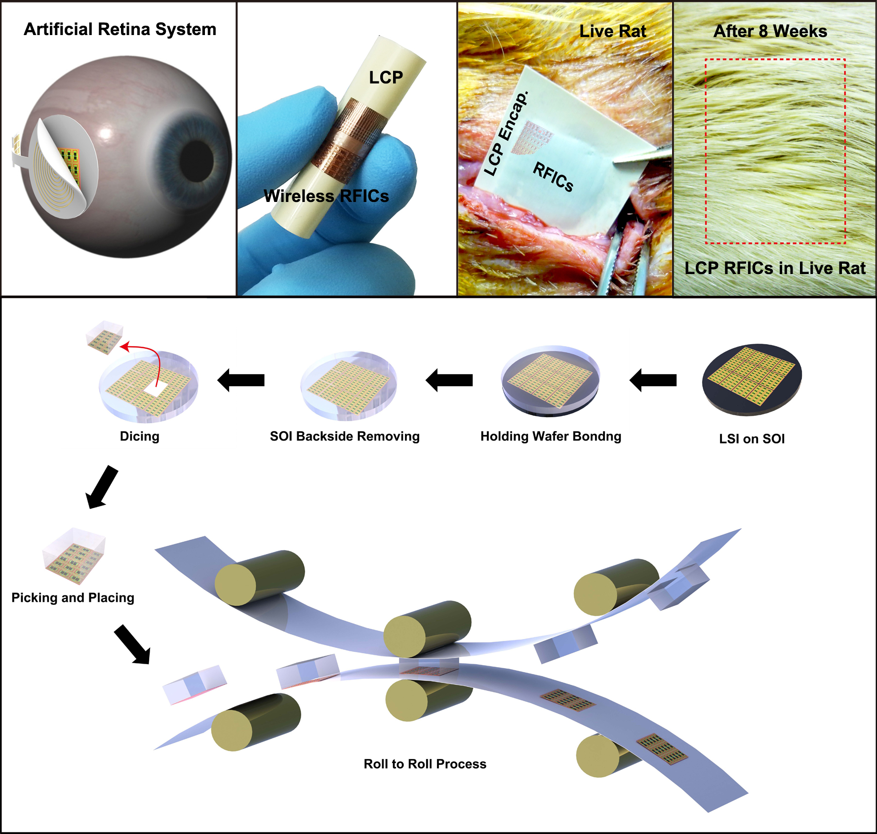 A KAIST research team developed in vivo flexible large scale integrated circuits
Daejeon, Republic of Korea, May 6th, 2013–-A team led by Professor Keon Jae Lee from the Department of Materials Science and Engineering at KAIST has developed in vivo silicon-based flexible large scale integrated circuits (LSI) for bio-medical wireless communication.
Silicon-based semiconductors have played significant roles in signal processing, nerve stimulation, memory storage, and wireless communication in implantable electronics. However, the rigid and bulky LSI chips have limited uses in in vivo devices due to incongruent contact with the curvilinear surfaces of human organs. Especially, artificial retinas recently approved by the Food and Drug Administration (refer to the press release of FDA"s artificial retina approval) require extremely flexible and slim LSI to incorporate it within the cramped area of the human eye.
Although several research teams have fabricated flexible integrated circuits (ICs, tens of interconnected transistors) on plastics, their inaccurate nano-scale alignment on plastics has restricted the demonstration of flexible nano-transistors and their large scale interconnection for in vivo LSI applications such as main process unit (MPU), high density memory and wireless communication. Professor Lee"s team previously demonstrated fully functional flexible memory using ultrathin silicon membranes (Nano Letters, Flexible Memristive Memory Array on Plastic Substrates), however, its integration level and transistor size (over micron scale) have limited functional applications for flexible consumer electronics.
Professor Keon Jae Lee"s team fabricated radio frequency integrated circuits (RFICs) interconnected with thousand nano-transistors on silicon wafer by state-of-the-art CMOS process, and then they removed the entire bottom substrate except top 100 nm active circuit layer by wet chemical etching. The flexible RF switches for wireless communication were monolithically encapsulated with biocompatible liquid crystal polymers (LCPs) for in vivo bio-medical applications. Finally, they implanted the LCP encapsulated RFICs into live rats to demonstrate the stable operation of flexible devices under in vivo circumstances.
Professor Lee said, "This work could provide an approach to flexible LSI for an ideal artificial retina system and other bio-medical devices. Moreover, the result represents an exciting technology with the strong potential to realize fully flexible consumer electronics such as application processor (AP) for mobile operating system, high-capacity memory, and wireless communication in the near future."
This result was published in the May online issue of the American Chemical Society"s journal, ACS Nano (In vivo Flexible RFICs Monolithically Encapsulated with LCP). They are currently engaged in commercializing efforts of roll-to-roll printing of flexible LSI on large area plastic substrates.
Movie at Youtube Link: Fabrication process for flexible LSI for flexible display, wearable computer and artificial retina for in vivo biomedical application
http://www.youtube.com/watch?v=5PpbM7m2PPs&feature=youtu.be
Applications of in Vivo Flexible Large Scale Integrated Circuits
Top: In vivo flexible large scale integrated circuits (LSI); Bottom: Schematic of roll-to-roll printing of flexible LSI on large area plastics.
2013.06.09 View 14545
A KAIST research team developed in vivo flexible large scale integrated circuits
Daejeon, Republic of Korea, May 6th, 2013–-A team led by Professor Keon Jae Lee from the Department of Materials Science and Engineering at KAIST has developed in vivo silicon-based flexible large scale integrated circuits (LSI) for bio-medical wireless communication.
Silicon-based semiconductors have played significant roles in signal processing, nerve stimulation, memory storage, and wireless communication in implantable electronics. However, the rigid and bulky LSI chips have limited uses in in vivo devices due to incongruent contact with the curvilinear surfaces of human organs. Especially, artificial retinas recently approved by the Food and Drug Administration (refer to the press release of FDA"s artificial retina approval) require extremely flexible and slim LSI to incorporate it within the cramped area of the human eye.
Although several research teams have fabricated flexible integrated circuits (ICs, tens of interconnected transistors) on plastics, their inaccurate nano-scale alignment on plastics has restricted the demonstration of flexible nano-transistors and their large scale interconnection for in vivo LSI applications such as main process unit (MPU), high density memory and wireless communication. Professor Lee"s team previously demonstrated fully functional flexible memory using ultrathin silicon membranes (Nano Letters, Flexible Memristive Memory Array on Plastic Substrates), however, its integration level and transistor size (over micron scale) have limited functional applications for flexible consumer electronics.
Professor Keon Jae Lee"s team fabricated radio frequency integrated circuits (RFICs) interconnected with thousand nano-transistors on silicon wafer by state-of-the-art CMOS process, and then they removed the entire bottom substrate except top 100 nm active circuit layer by wet chemical etching. The flexible RF switches for wireless communication were monolithically encapsulated with biocompatible liquid crystal polymers (LCPs) for in vivo bio-medical applications. Finally, they implanted the LCP encapsulated RFICs into live rats to demonstrate the stable operation of flexible devices under in vivo circumstances.
Professor Lee said, "This work could provide an approach to flexible LSI for an ideal artificial retina system and other bio-medical devices. Moreover, the result represents an exciting technology with the strong potential to realize fully flexible consumer electronics such as application processor (AP) for mobile operating system, high-capacity memory, and wireless communication in the near future."
This result was published in the May online issue of the American Chemical Society"s journal, ACS Nano (In vivo Flexible RFICs Monolithically Encapsulated with LCP). They are currently engaged in commercializing efforts of roll-to-roll printing of flexible LSI on large area plastic substrates.
Movie at Youtube Link: Fabrication process for flexible LSI for flexible display, wearable computer and artificial retina for in vivo biomedical application
http://www.youtube.com/watch?v=5PpbM7m2PPs&feature=youtu.be
Applications of in Vivo Flexible Large Scale Integrated Circuits
Top: In vivo flexible large scale integrated circuits (LSI); Bottom: Schematic of roll-to-roll printing of flexible LSI on large area plastics.
2013.06.09 View 14545 -
 Professor Lee Jeong Yong Receives 2012 'KAISTian of the Year' Award
Professor Lee Jeong Yong (Department of Material Science and Engineering) received the 2012 ‘KAISTian of the Year’ Award.
Professor Lee had successfully developed a technique that allowed the observation and analysis of liquid in atomic scale.
The technique is expected to have great impact on nano-material synthesis in solution, explaining electrode and electrolyte reaction, liquid and catalysis reaction research, and etc. and was therefore named as the best experimental accomplishment in KAIST in 2012.
Professor Lee and his team’s finding has been published in the April edition of Science magazine and has had attracted the attention of the world. In addition, BBC News, and Science & Environment reported on the findings as their respective top articles.
The optical microscope is incapable of atomic scale observation and the electron microscopes are capable but because of the vacuum state all liquids undergo evaporation making it impossible to observe liquids in an atomic scale.
Professor Lee’s team wrapped the liquid with a layer of grapheme to prevent evaporation and successfully observed real time the platinum growth process in solution.
Professor Lee’s findings were introduced as an example of exemplar research case in the Presidential address for ‘Science Day’ in April.
2013.01.22 View 9922
Professor Lee Jeong Yong Receives 2012 'KAISTian of the Year' Award
Professor Lee Jeong Yong (Department of Material Science and Engineering) received the 2012 ‘KAISTian of the Year’ Award.
Professor Lee had successfully developed a technique that allowed the observation and analysis of liquid in atomic scale.
The technique is expected to have great impact on nano-material synthesis in solution, explaining electrode and electrolyte reaction, liquid and catalysis reaction research, and etc. and was therefore named as the best experimental accomplishment in KAIST in 2012.
Professor Lee and his team’s finding has been published in the April edition of Science magazine and has had attracted the attention of the world. In addition, BBC News, and Science & Environment reported on the findings as their respective top articles.
The optical microscope is incapable of atomic scale observation and the electron microscopes are capable but because of the vacuum state all liquids undergo evaporation making it impossible to observe liquids in an atomic scale.
Professor Lee’s team wrapped the liquid with a layer of grapheme to prevent evaporation and successfully observed real time the platinum growth process in solution.
Professor Lee’s findings were introduced as an example of exemplar research case in the Presidential address for ‘Science Day’ in April.
2013.01.22 View 9922 -
 Professor Cho Young-ho wins 'E2 Star' award
Professor Cho Young-ho from the Department of Bio and Brain Engineering at KAIST was chosen as the ‘E2 Star’ at the ‘2012 Engineering Education Festa’ in academics. The ‘2012 Engineering Education Festa’ hosted by the Ministry of Education, Science and Technology was held to display outstanding research results and to conceptualize the future of science education.
The ‘E2 star’ award is given to renowned figures in industry, academia and society. A total of 35 candidates were recommended for the 3 fields and Professor Cho received the first place in the online voting.
Professor Cho received high marks for his work in engineering education, research development and increasing the communication between academia and industry, as well as the commercialization of science and technology. Professor Cho was especially praised for the specialization of engineering education in integrated fields and the joint research with US and Swiss universities.
Professor Cho Young-ho(Department of Bio and Brain Engineering, KAIST)
2012.12.26 View 11369
Professor Cho Young-ho wins 'E2 Star' award
Professor Cho Young-ho from the Department of Bio and Brain Engineering at KAIST was chosen as the ‘E2 Star’ at the ‘2012 Engineering Education Festa’ in academics. The ‘2012 Engineering Education Festa’ hosted by the Ministry of Education, Science and Technology was held to display outstanding research results and to conceptualize the future of science education.
The ‘E2 star’ award is given to renowned figures in industry, academia and society. A total of 35 candidates were recommended for the 3 fields and Professor Cho received the first place in the online voting.
Professor Cho received high marks for his work in engineering education, research development and increasing the communication between academia and industry, as well as the commercialization of science and technology. Professor Cho was especially praised for the specialization of engineering education in integrated fields and the joint research with US and Swiss universities.
Professor Cho Young-ho(Department of Bio and Brain Engineering, KAIST)
2012.12.26 View 11369 -
Flexible Nanogenerator Technology
KAIST research team successfully developed the foundation technology that will enable to fabrication of low cost, large area nanogenerator.
Professor Lee Gun Jae’s team (Department of Materials Science and Engineering) published a dissertation on a nanogenerator using nanocomplexes as the cover dissertation of the June edition of Advanced Materials.
The developed technology is receiving rave reviews for having overcome the complex and size limitations of the nanogenerator fabrication process.
A nanogenerator is an electricity generator that uses materials in the nanoscale and uses piezoelectricity that creates electricity with the application of physical force.
The generation technology using piezoelectricity was appointed as one of top 10 promising technologies by MIT in 2009 and was included in the 45 innovative technologies that will shake the world by Popular Science Magazine in 2010.
The only nanogenerator thus far was the ZnO model suggested by Georgia Tech’s Professor Zhong Lin Wang in 2005.
Professor Lee’s team used ceramic thin film material BaTiO3 which has 15~20 times greater piezoelectric capacity than ZnO and thus improved the overall performance of the device. The use of a nanocomplex allows large scale production and the simplification of the fabrication process itself.
The team created a mixture of PDMS (polydimethylsiloxane) with BaTiO3 and either of CNT (Carbon Nanotube) or RGO (Reduced Graphene Oxide) which has high electrical conductivity and applied this mixture to create a large scale nanogenerator.
2012.06.18 View 14465
-
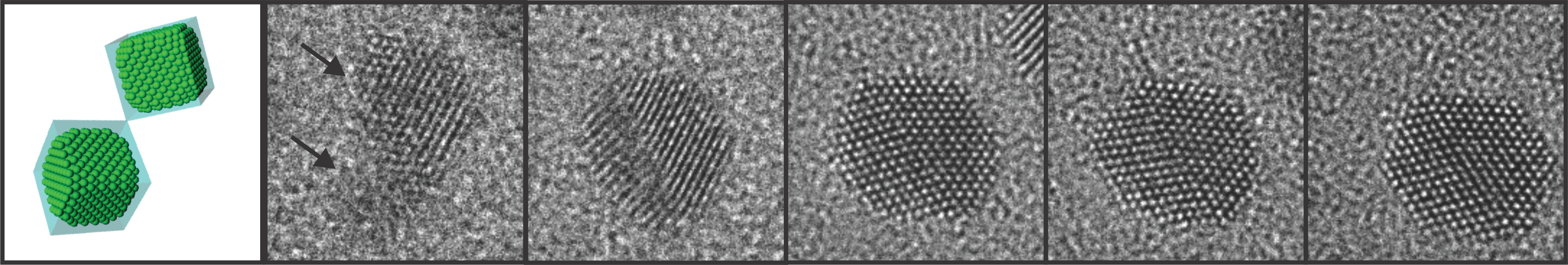 High-resolution Atomic Imaging of Specimens in Liquid Observed by Transmission Electron Microscopes Using Graphene Liquid Cells
Looking into specimens in liquid at the atomic level to understand nanoscale processes so far regarded as impossible to witnessThe Korea Advanced Institute of Science and Technology (KAIST) announced that a research team from the Department of Materials Science and Engineering has developed a technology that enables scientists and engineers to observe processes occurring in liquid media on the smallest possible scale which is less than a nanometer.
Professor Jeong Yong Lee and Researcher Jong Min Yuk, in collaboration with Professors Paul Alivisatos’s and Alex Zettl’s groups at the University of California, Berkeley, succeeded in making a graphene liquid cell or capsule, confining an ultra-thin liquid film between layers of graphene, for real-time and in situ imagining of nanoscale processes in fluids with atomic-level resolution by a transmission electron microscope (TEM). Their research was published in the April 6, 2012 issue of Science. (http://www.sciencemag.org/content/336/6077/61.abstract)
The graphene liquid cell (GLC) is composed of two sheets of graphene sandwiched to create a sealed chamber where a platinum growth solution is encapsulated in the form of a thin slice. Each graphene layer has a thickness of one carbon atom, the thinnest membrane that has ever been used to fabricate a liquid cell required for TEM.
The research team peered inside the GLC to observe the growth and dynamics of platinum nanocrystals in solution as they coalesced into a larger size, during which the graphene membrane with the encapsulated liquid remained intact. The researchers from KAIST and the UC Berkeley identified important features in the ongoing process of the nanocrystals’ coalescence and their expansion through coalescence to form certain shapes by imaging the phenomena with atomic-level resolution.
Professor Lee said,
“It has now become possible for scientists to observe what is happening in liquids on an atomic level under transmission electron microscopes.”
Researcher Yuk, one of the first authors of the paper, explained his research work.
“This research will promote other fields of study related to materials in a fluid stage including physical, chemical, and biological phenomena at the atomic level and promises numerous applications in the future. Pending further studies on liquid microscopy, the full application of a graphene-liquid-cell (GLC) TEM to biological samples is yet to be confirmed. Nonetheless, the GLC is the most effective technique developed today to sustain the natural state of fluid samples or species suspended in the liquid for a TEM imaging.”
The transmission electron microscope (TEM), first introduced in the 1930s, produces images at a significantly higher resolution than light microscopes, allowing users to examine the smallest level of physical, chemical, and biological phenomena. Observations by TEM with atomic resolution, however, have been limited to solid and/or frozen samples, and thus it has previously been impossible to study the real time fluid dynamics of liquid phases.
TEM imaging is performed in a high vacuum chamber in which a thin slice of the imaged sample is situated, and an electron beam passes through the slice to create an image. In this process, a liquid medium, unlike solid or frozen samples, evaporates, making it difficult to observe under TEM.
Attempts to produce a liquid capsule have thus far been made with electron-transparent membranes of such materials as silicon nitride or silicon oxide; such liquid capsules are relatively thick (tens to one hundred nanometers), however, resulting in poor electron transmittance with a reduced resolution of only a few nanometers. Silicon nitride is 25 nanometers thick, whereas graphene is only 0.34 nanometers.
Graphene, most commonly found in bulk graphite, is the thinnest material made out of carbon atoms. It has unique properties such as mechanical tensile strength, high flexibility, impermeability to small molecules, and high electrical conductivity. Graphene is an excellent material to hold micro- and nanoscopic objects for observation in a transmission electron microscope by minimizing scattering of the electron beam that irradiates a liquid sample while reducing charging and heating effects.
###
Figure 1. Schematic illustration of graphene liquid cells. Sandwiched two sheets of graphene encapsulate a platinum growth solution.
Figure 2. In-situ TEM observation of nanocrystal growth and shape evolution. TEM images of platinum nanocrystal coalescence and their faceting in the growth solution.
2012.04.23 View 12693
High-resolution Atomic Imaging of Specimens in Liquid Observed by Transmission Electron Microscopes Using Graphene Liquid Cells
Looking into specimens in liquid at the atomic level to understand nanoscale processes so far regarded as impossible to witnessThe Korea Advanced Institute of Science and Technology (KAIST) announced that a research team from the Department of Materials Science and Engineering has developed a technology that enables scientists and engineers to observe processes occurring in liquid media on the smallest possible scale which is less than a nanometer.
Professor Jeong Yong Lee and Researcher Jong Min Yuk, in collaboration with Professors Paul Alivisatos’s and Alex Zettl’s groups at the University of California, Berkeley, succeeded in making a graphene liquid cell or capsule, confining an ultra-thin liquid film between layers of graphene, for real-time and in situ imagining of nanoscale processes in fluids with atomic-level resolution by a transmission electron microscope (TEM). Their research was published in the April 6, 2012 issue of Science. (http://www.sciencemag.org/content/336/6077/61.abstract)
The graphene liquid cell (GLC) is composed of two sheets of graphene sandwiched to create a sealed chamber where a platinum growth solution is encapsulated in the form of a thin slice. Each graphene layer has a thickness of one carbon atom, the thinnest membrane that has ever been used to fabricate a liquid cell required for TEM.
The research team peered inside the GLC to observe the growth and dynamics of platinum nanocrystals in solution as they coalesced into a larger size, during which the graphene membrane with the encapsulated liquid remained intact. The researchers from KAIST and the UC Berkeley identified important features in the ongoing process of the nanocrystals’ coalescence and their expansion through coalescence to form certain shapes by imaging the phenomena with atomic-level resolution.
Professor Lee said,
“It has now become possible for scientists to observe what is happening in liquids on an atomic level under transmission electron microscopes.”
Researcher Yuk, one of the first authors of the paper, explained his research work.
“This research will promote other fields of study related to materials in a fluid stage including physical, chemical, and biological phenomena at the atomic level and promises numerous applications in the future. Pending further studies on liquid microscopy, the full application of a graphene-liquid-cell (GLC) TEM to biological samples is yet to be confirmed. Nonetheless, the GLC is the most effective technique developed today to sustain the natural state of fluid samples or species suspended in the liquid for a TEM imaging.”
The transmission electron microscope (TEM), first introduced in the 1930s, produces images at a significantly higher resolution than light microscopes, allowing users to examine the smallest level of physical, chemical, and biological phenomena. Observations by TEM with atomic resolution, however, have been limited to solid and/or frozen samples, and thus it has previously been impossible to study the real time fluid dynamics of liquid phases.
TEM imaging is performed in a high vacuum chamber in which a thin slice of the imaged sample is situated, and an electron beam passes through the slice to create an image. In this process, a liquid medium, unlike solid or frozen samples, evaporates, making it difficult to observe under TEM.
Attempts to produce a liquid capsule have thus far been made with electron-transparent membranes of such materials as silicon nitride or silicon oxide; such liquid capsules are relatively thick (tens to one hundred nanometers), however, resulting in poor electron transmittance with a reduced resolution of only a few nanometers. Silicon nitride is 25 nanometers thick, whereas graphene is only 0.34 nanometers.
Graphene, most commonly found in bulk graphite, is the thinnest material made out of carbon atoms. It has unique properties such as mechanical tensile strength, high flexibility, impermeability to small molecules, and high electrical conductivity. Graphene is an excellent material to hold micro- and nanoscopic objects for observation in a transmission electron microscope by minimizing scattering of the electron beam that irradiates a liquid sample while reducing charging and heating effects.
###
Figure 1. Schematic illustration of graphene liquid cells. Sandwiched two sheets of graphene encapsulate a platinum growth solution.
Figure 2. In-situ TEM observation of nanocrystal growth and shape evolution. TEM images of platinum nanocrystal coalescence and their faceting in the growth solution.
2012.04.23 View 12693