electron
-
 Atomically-Smooth Gold Crystals Help to Compress Light for Nanophotonic Applications
Highly compressed mid-infrared optical waves in a thin dielectric crystal on monocrystalline gold substrate investigated for the first time using a high-resolution scattering-type scanning near-field optical microscope.
KAIST researchers and their collaborators at home and abroad have successfully demonstrated a new platform for guiding the compressed light waves in very thin van der Waals crystals. Their method to guide the mid-infrared light with minimal loss will provide a breakthrough for the practical applications of ultra-thin dielectric crystals in next-generation optoelectronic devices based on strong light-matter interactions at the nanoscale.
Phonon-polaritons are collective oscillations of ions in polar dielectrics coupled to electromagnetic waves of light, whose electromagnetic field is much more compressed compared to the light wavelength. Recently, it was demonstrated that the phonon-polaritons in thin van der Waals crystals can be compressed even further when the material is placed on top of a highly conductive metal. In such a configuration, charges in the polaritonic crystal are “reflected” in the metal, and their coupling with light results in a new type of polariton waves called the image phonon-polaritons. Highly compressed image modes provide strong light-matter interactions, but are very sensitive to the substrate roughness, which hinders their practical application.
Challenged by these limitations, four research groups combined their efforts to develop a unique experimental platform using advanced fabrication and measurement methods. Their findings were published in Science Advances on July 13.
A KAIST research team led by Professor Min Seok Jang from the School of Electrical Engineering used a highly sensitive scanning near-field optical microscope (SNOM) to directly measure the optical fields of the hyperbolic image phonon-polaritons (HIP) propagating in a 63 nm-thick slab of hexagonal boron nitride (h-BN) on a monocrystalline gold substrate, showing the mid-infrared light waves in dielectric crystal compressed by a hundred times.
Professor Jang and a research professor in his group, Sergey Menabde, successfully obtained direct images of HIP waves propagating for many wavelengths, and detected a signal from the ultra-compressed high-order HIP in a regular h-BN crystals for the first time. They showed that the phonon-polaritons in van der Waals crystals can be significantly more compressed without sacrificing their lifetime.
This became possible due to the atomically-smooth surfaces of the home-grown gold crystals used as a substrate for the h-BN. Practically zero surface scattering and extremely small ohmic loss in gold at mid-infrared frequencies provide a low-loss environment for the HIP propagation. The HIP mode probed by the researchers was 2.4 times more compressed and yet exhibited a similar lifetime compared to the phonon-polaritons with a low-loss dielectric substrate, resulting in a twice higher figure of merit in terms of the normalized propagation length.
The ultra-smooth monocrystalline gold flakes used in the experiment were chemically grown by the team of Professor N. Asger Mortensen from the Center for Nano Optics at the University of Southern Denmark.
Mid-infrared spectrum is particularly important for sensing applications since many important organic molecules have absorption lines in the mid-infrared. However, a large number of molecules is required by the conventional detection methods for successful operation, whereas the ultra-compressed phonon-polariton fields can provide strong light-matter interactions at the microscopic level, thus significantly improving the detection limit down to a single molecule. The long lifetime of the HIP on monocrystalline gold will further improve the detection performance.
Furthermore, the study conducted by Professor Jang and the team demonstrated the striking similarity between the HIP and the image graphene plasmons. Both image modes possess significantly more confined electromagnetic field, yet their lifetime remains unaffected by the shorter polariton wavelength. This observation provides a broader perspective on image polaritons in general, and highlights their superiority in terms of the nanolight waveguiding compared to the conventional low-dimensional polaritons in van der Waals crystals on a dielectric substrate.
Professor Jang said, “Our research demonstrated the advantages of image polaritons, and especially the image phonon-polaritons. These optical modes can be used in the future optoelectronic devices where both the low-loss propagation and the strong light-matter interaction are necessary. I hope that our results will pave the way for the realization of more efficient nanophotonic devices such as metasurfaces, optical switches, sensors, and other applications operating at infrared frequencies.”
This research was funded by the Samsung Research Funding & Incubation Center of Samsung Electronics and the National Research Foundation of Korea (NRF). The Korea Institute of Science and Technology, Ministry of Education, Culture, Sports, Science and Technology of Japan, and The Villum Foundation, Denmark, also supported the work.
Figure. Nano-tip is used for the ultra-high-resolution imaging of the image phonon-polaritons in hBN launched by the gold crystal edge.
Publication:
Menabde, S. G., et al. (2022) Near-field probing of image phonon-polaritons in hexagonal boron nitride on gold crystals. Science Advances 8, Article ID: eabn0627. Available online at https://science.org/doi/10.1126/sciadv.abn0627.
Profile:
Min Seok Jang, MS, PhD
Associate Professor
jang.minseok@kaist.ac.kr
http://janglab.org/
Min Seok Jang Research Group
School of Electrical Engineering
http://kaist.ac.kr/en/
Korea Advanced Institute of Science and Technology (KAIST)
Daejeon, Republic of Korea
2022.07.13 View 16614
Atomically-Smooth Gold Crystals Help to Compress Light for Nanophotonic Applications
Highly compressed mid-infrared optical waves in a thin dielectric crystal on monocrystalline gold substrate investigated for the first time using a high-resolution scattering-type scanning near-field optical microscope.
KAIST researchers and their collaborators at home and abroad have successfully demonstrated a new platform for guiding the compressed light waves in very thin van der Waals crystals. Their method to guide the mid-infrared light with minimal loss will provide a breakthrough for the practical applications of ultra-thin dielectric crystals in next-generation optoelectronic devices based on strong light-matter interactions at the nanoscale.
Phonon-polaritons are collective oscillations of ions in polar dielectrics coupled to electromagnetic waves of light, whose electromagnetic field is much more compressed compared to the light wavelength. Recently, it was demonstrated that the phonon-polaritons in thin van der Waals crystals can be compressed even further when the material is placed on top of a highly conductive metal. In such a configuration, charges in the polaritonic crystal are “reflected” in the metal, and their coupling with light results in a new type of polariton waves called the image phonon-polaritons. Highly compressed image modes provide strong light-matter interactions, but are very sensitive to the substrate roughness, which hinders their practical application.
Challenged by these limitations, four research groups combined their efforts to develop a unique experimental platform using advanced fabrication and measurement methods. Their findings were published in Science Advances on July 13.
A KAIST research team led by Professor Min Seok Jang from the School of Electrical Engineering used a highly sensitive scanning near-field optical microscope (SNOM) to directly measure the optical fields of the hyperbolic image phonon-polaritons (HIP) propagating in a 63 nm-thick slab of hexagonal boron nitride (h-BN) on a monocrystalline gold substrate, showing the mid-infrared light waves in dielectric crystal compressed by a hundred times.
Professor Jang and a research professor in his group, Sergey Menabde, successfully obtained direct images of HIP waves propagating for many wavelengths, and detected a signal from the ultra-compressed high-order HIP in a regular h-BN crystals for the first time. They showed that the phonon-polaritons in van der Waals crystals can be significantly more compressed without sacrificing their lifetime.
This became possible due to the atomically-smooth surfaces of the home-grown gold crystals used as a substrate for the h-BN. Practically zero surface scattering and extremely small ohmic loss in gold at mid-infrared frequencies provide a low-loss environment for the HIP propagation. The HIP mode probed by the researchers was 2.4 times more compressed and yet exhibited a similar lifetime compared to the phonon-polaritons with a low-loss dielectric substrate, resulting in a twice higher figure of merit in terms of the normalized propagation length.
The ultra-smooth monocrystalline gold flakes used in the experiment were chemically grown by the team of Professor N. Asger Mortensen from the Center for Nano Optics at the University of Southern Denmark.
Mid-infrared spectrum is particularly important for sensing applications since many important organic molecules have absorption lines in the mid-infrared. However, a large number of molecules is required by the conventional detection methods for successful operation, whereas the ultra-compressed phonon-polariton fields can provide strong light-matter interactions at the microscopic level, thus significantly improving the detection limit down to a single molecule. The long lifetime of the HIP on monocrystalline gold will further improve the detection performance.
Furthermore, the study conducted by Professor Jang and the team demonstrated the striking similarity between the HIP and the image graphene plasmons. Both image modes possess significantly more confined electromagnetic field, yet their lifetime remains unaffected by the shorter polariton wavelength. This observation provides a broader perspective on image polaritons in general, and highlights their superiority in terms of the nanolight waveguiding compared to the conventional low-dimensional polaritons in van der Waals crystals on a dielectric substrate.
Professor Jang said, “Our research demonstrated the advantages of image polaritons, and especially the image phonon-polaritons. These optical modes can be used in the future optoelectronic devices where both the low-loss propagation and the strong light-matter interaction are necessary. I hope that our results will pave the way for the realization of more efficient nanophotonic devices such as metasurfaces, optical switches, sensors, and other applications operating at infrared frequencies.”
This research was funded by the Samsung Research Funding & Incubation Center of Samsung Electronics and the National Research Foundation of Korea (NRF). The Korea Institute of Science and Technology, Ministry of Education, Culture, Sports, Science and Technology of Japan, and The Villum Foundation, Denmark, also supported the work.
Figure. Nano-tip is used for the ultra-high-resolution imaging of the image phonon-polaritons in hBN launched by the gold crystal edge.
Publication:
Menabde, S. G., et al. (2022) Near-field probing of image phonon-polaritons in hexagonal boron nitride on gold crystals. Science Advances 8, Article ID: eabn0627. Available online at https://science.org/doi/10.1126/sciadv.abn0627.
Profile:
Min Seok Jang, MS, PhD
Associate Professor
jang.minseok@kaist.ac.kr
http://janglab.org/
Min Seok Jang Research Group
School of Electrical Engineering
http://kaist.ac.kr/en/
Korea Advanced Institute of Science and Technology (KAIST)
Daejeon, Republic of Korea
2022.07.13 View 16614 -
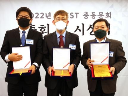 KAA Recognizes 4 Distinguished Alumni of the Year
The KAIST Alumni Association (KAA) recognized four distinguished alumni of the year during a ceremony on February 25 in Seoul. The four Distinguished Alumni Awardees are Distinguished Professor Sukbok Chang from the KAIST Department of Chemistry, Hyunshil Ahn, head of the AI Economy Institute and an editorial writer at The Korea Economic Daily, CEO Hwan-ho Sung of PSTech, and President Hark Kyu Park of Samsung Electronics.
Distinguished Professor Sukbok Chang who received his MS from the Department of Chemistry in 1985 has been a pioneer in the novel field of ‘carbon-hydrogen bond activation reactions’. He has significantly contributed to raising Korea’s international reputation in natural sciences and received the Kyungam Academic Award in 2013, the 14th Korea Science Award in 2015, the 1st Science and Technology Prize of Korea Toray in 2018, and the Best Scientist/Engineer Award Korea in 2019. Furthermore, he was named as a Highly Cited Researcher who ranked in the top 1% of citations by field and publication year in the Web of Science citation index for seven consecutive years from 2015 to 2021, demonstrating his leadership as a global scholar.
Hyunshil Ahn, a graduate of the School of Business and Technology Management with an MS in 1985 and a PhD in 1987, was appointed as the first head of the AI Economy Institute when The Korea Economic Daily was the first Korean media outlet to establish an AI economy lab. He has contributed to creating new roles for the press and media in the 4th industrial revolution, and added to the popularization of AI technology through regulation reform and consulting on industrial policies.
PSTech CEO Hwan-ho Sung is a graduate of the School of Electrical Engineering where he received an MS in 1988 and a PhD in EMBA in 2008. He has run the electronics company PSTech for over 20 years and successfully localized the production of power equipment, which previously depended on foreign technology. His development of the world’s first power equipment that can be applied to new industries including semiconductors and displays was recognized through this award.
Samsung Electronics President Hark Kyu Park graduated from the School of Business and Technology Management with an MS in 1986. He not only enhanced Korea’s national competitiveness by expanding the semiconductor industry, but also established contract-based semiconductor departments at Korean universities including KAIST, Sungkyunkwan University, Yonsei University, and Postech, and semiconductor track courses at KAIST, Sogang University, Seoul National University, and Postech to nurture professional talents. He also led the national semiconductor coexistence system by leading private sector-government-academia collaborations to strengthen competence in semiconductors, and continues to make unconditional investments in strong small businesses.
KAA President Chilhee Chung said, “Thanks to our alumni contributing at the highest levels of our society, the name of our alma mater shines brighter. As role models for our younger alumni, I hope greater honours will follow our awardees in the future.”
2022.03.03 View 9442
KAA Recognizes 4 Distinguished Alumni of the Year
The KAIST Alumni Association (KAA) recognized four distinguished alumni of the year during a ceremony on February 25 in Seoul. The four Distinguished Alumni Awardees are Distinguished Professor Sukbok Chang from the KAIST Department of Chemistry, Hyunshil Ahn, head of the AI Economy Institute and an editorial writer at The Korea Economic Daily, CEO Hwan-ho Sung of PSTech, and President Hark Kyu Park of Samsung Electronics.
Distinguished Professor Sukbok Chang who received his MS from the Department of Chemistry in 1985 has been a pioneer in the novel field of ‘carbon-hydrogen bond activation reactions’. He has significantly contributed to raising Korea’s international reputation in natural sciences and received the Kyungam Academic Award in 2013, the 14th Korea Science Award in 2015, the 1st Science and Technology Prize of Korea Toray in 2018, and the Best Scientist/Engineer Award Korea in 2019. Furthermore, he was named as a Highly Cited Researcher who ranked in the top 1% of citations by field and publication year in the Web of Science citation index for seven consecutive years from 2015 to 2021, demonstrating his leadership as a global scholar.
Hyunshil Ahn, a graduate of the School of Business and Technology Management with an MS in 1985 and a PhD in 1987, was appointed as the first head of the AI Economy Institute when The Korea Economic Daily was the first Korean media outlet to establish an AI economy lab. He has contributed to creating new roles for the press and media in the 4th industrial revolution, and added to the popularization of AI technology through regulation reform and consulting on industrial policies.
PSTech CEO Hwan-ho Sung is a graduate of the School of Electrical Engineering where he received an MS in 1988 and a PhD in EMBA in 2008. He has run the electronics company PSTech for over 20 years and successfully localized the production of power equipment, which previously depended on foreign technology. His development of the world’s first power equipment that can be applied to new industries including semiconductors and displays was recognized through this award.
Samsung Electronics President Hark Kyu Park graduated from the School of Business and Technology Management with an MS in 1986. He not only enhanced Korea’s national competitiveness by expanding the semiconductor industry, but also established contract-based semiconductor departments at Korean universities including KAIST, Sungkyunkwan University, Yonsei University, and Postech, and semiconductor track courses at KAIST, Sogang University, Seoul National University, and Postech to nurture professional talents. He also led the national semiconductor coexistence system by leading private sector-government-academia collaborations to strengthen competence in semiconductors, and continues to make unconditional investments in strong small businesses.
KAA President Chilhee Chung said, “Thanks to our alumni contributing at the highest levels of our society, the name of our alma mater shines brighter. As role models for our younger alumni, I hope greater honours will follow our awardees in the future.”
2022.03.03 View 9442 -
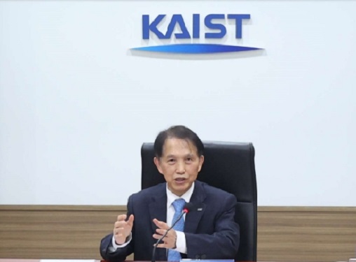 President Lee Presents Plans to Nurture Next-Generation Talents
President Lee stressed that nurturing medical scientists, semiconductor R&D personnel, startup entrepreneurs, and global innovators are key missions he will continue to pursue during a news conference
KAIST President Kwang Hyung Lee said that nurturing medical scientists, semiconductor R&D personnel, startup entrepreneurs, and global innovators are key missions he will continue to pursue during an online news conference marking the 1st anniversary of him becoming the president on February 15.
He said that nurturing physician-scientists is the most critical mission for KAIST to help the nation create a new growth engine. He said KAIST will help the nation drive the bio-industry and provide medical science resources for the nation’s health sector. To this end, he said that KAIST will open its Medical Science and Technology School by 2026.
“We plan to expand the current Graduate School of Medical Science and Engineering into a new Medical Science and Technology School that will focus entirely on a condensed MD-PhD course converging the fields of AI, bio, and physics,” he said.
The school aims to foster medical scientists whose research results will eventually be commercialized. He said that the university is now discussing revisions to related laws and regulations with the government and other universities.
To supply human resources to the semiconductor industry, President Lee said the university will add a campus in Pyongtaek City that will serve as an advanced convergence research hub in the field of next generation semiconductors in collaboration with Samsung Electronics and the city of Pyongtaek. The three-stage opening plan projected the final opening of the campus by 2036. During the first stage, which will be completed by 2026, it will construct the campus infrastructure in Pyongtaek city where Samsung Semiconductors runs two massive semiconductor complexes. By 2031, it plans to launch the open research platform including a future cities research center and future vehicles research center. The campus will open the global industrial collaboration cluster hub by 2036.
In the global arena, President Lee said he is working to open the New York campus with stakeholders in the United States. He announced the plan last December that was endorsed by New York-based entrepreneur Hee-Nam Bae, the chairman of Big Continent Inc. President Lee and Chairman Lee signed an MOU for the funding to open the campus in New York.
“We are discussing how to facilitate the plan and best accommodate the interests and potential of our students. Many ideas and plans are on the table and we think it will take longer than expected to finalize the plan,” explained President Lee.
However, he added that the basic idea is to offer art tech and health technology programs as well as an AI-based finance MBA at the New York campus, in addition to it serving as the startup accelerator of KAIST.
President Lee stressed the importance of technology commercialization when successfully launching KAIST Holdings last month to help spinoffs of KAIST labs accelerate their end results. He said that KAIST Holdings will build a virtuous supporting system to commercialize the technology startups coming from KAIST.
“We plan to list at least 10 KAIST startups on the KOSDAQ and two on the NASDAQ by 2031. KAIST Holdings also aims to nurture companies valued at a total of one billion KRW and earn 100 billion KRW in technology fees by 2031.
2022.02.17 View 13609
President Lee Presents Plans to Nurture Next-Generation Talents
President Lee stressed that nurturing medical scientists, semiconductor R&D personnel, startup entrepreneurs, and global innovators are key missions he will continue to pursue during a news conference
KAIST President Kwang Hyung Lee said that nurturing medical scientists, semiconductor R&D personnel, startup entrepreneurs, and global innovators are key missions he will continue to pursue during an online news conference marking the 1st anniversary of him becoming the president on February 15.
He said that nurturing physician-scientists is the most critical mission for KAIST to help the nation create a new growth engine. He said KAIST will help the nation drive the bio-industry and provide medical science resources for the nation’s health sector. To this end, he said that KAIST will open its Medical Science and Technology School by 2026.
“We plan to expand the current Graduate School of Medical Science and Engineering into a new Medical Science and Technology School that will focus entirely on a condensed MD-PhD course converging the fields of AI, bio, and physics,” he said.
The school aims to foster medical scientists whose research results will eventually be commercialized. He said that the university is now discussing revisions to related laws and regulations with the government and other universities.
To supply human resources to the semiconductor industry, President Lee said the university will add a campus in Pyongtaek City that will serve as an advanced convergence research hub in the field of next generation semiconductors in collaboration with Samsung Electronics and the city of Pyongtaek. The three-stage opening plan projected the final opening of the campus by 2036. During the first stage, which will be completed by 2026, it will construct the campus infrastructure in Pyongtaek city where Samsung Semiconductors runs two massive semiconductor complexes. By 2031, it plans to launch the open research platform including a future cities research center and future vehicles research center. The campus will open the global industrial collaboration cluster hub by 2036.
In the global arena, President Lee said he is working to open the New York campus with stakeholders in the United States. He announced the plan last December that was endorsed by New York-based entrepreneur Hee-Nam Bae, the chairman of Big Continent Inc. President Lee and Chairman Lee signed an MOU for the funding to open the campus in New York.
“We are discussing how to facilitate the plan and best accommodate the interests and potential of our students. Many ideas and plans are on the table and we think it will take longer than expected to finalize the plan,” explained President Lee.
However, he added that the basic idea is to offer art tech and health technology programs as well as an AI-based finance MBA at the New York campus, in addition to it serving as the startup accelerator of KAIST.
President Lee stressed the importance of technology commercialization when successfully launching KAIST Holdings last month to help spinoffs of KAIST labs accelerate their end results. He said that KAIST Holdings will build a virtuous supporting system to commercialize the technology startups coming from KAIST.
“We plan to list at least 10 KAIST startups on the KOSDAQ and two on the NASDAQ by 2031. KAIST Holdings also aims to nurture companies valued at a total of one billion KRW and earn 100 billion KRW in technology fees by 2031.
2022.02.17 View 13609 -
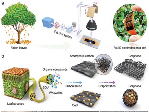 Eco-Friendly Micro-Supercapacitors Using Fallen Leaves
Green micro-supercapacitors on a single leaf could easily be applied in wearable electronics, smart houses, and IoTs
A KAIST research team has developed graphene-inorganic-hybrid micro-supercapacitors made of fallen leaves using femtosecond laser direct writing. The rapid development of wearable electronics requires breakthrough innovations in flexible energy storage devices in which micro-supercapacitors have drawn a great deal of interest due to their high power density, long lifetimes, and short charging times. Recently, there has been an enormous increase in waste batteries owing to the growing demand and the shortened replacement cycle in consumer electronics. The safety and environmental issues involved in the collection, recycling, and processing of such waste batteries are creating a number of challenges.
Forests cover about 30 percent of the Earth’s surface and produce a huge amount of fallen leaves. This naturally occurring biomass comes in large quantities and is completely biodegradable, which makes it an attractive sustainable resource. Nevertheless, if the fallen leaves are left neglected instead of being used efficiently, they can contribute to fire hazards, air pollution, and global warming.
To solve both problems at once, a research team led by Professor Young-Jin Kim from the Department of Mechanical Engineering and Dr. Hana Yoon from the Korea Institute of Energy Research developed a novel technology that can create 3D porous graphene microelectrodes with high electrical conductivity by irradiating femtosecond laser pulses on the leaves in ambient air. This one-step fabrication does not require any additional materials or pre-treatment.
They showed that this technique could quickly and easily produce porous graphene electrodes at a low price, and demonstrated potential applications by fabricating graphene micro-supercapacitors to power an LED and an electronic watch. These results open up a new possibility for the mass production of flexible and green graphene-based electronic devices.
Professor Young-Jin Kim said, “Leaves create forest biomass that comes in unmanageable quantities, so using them for next-generation energy storage devices makes it possible for us to reuse waste resources, thereby establishing a virtuous cycle.”
This research was published in Advanced Functional Materials last month and was sponsored by the Ministry of Agriculture Food and Rural Affairs, the Korea Forest Service, and the Korea Institute of Energy Research.
-Publication
Truong-Son Dinh Le, Yeong A. Lee, Han Ku Nam, Kyu Yeon Jang, Dongwook Yang, Byunggi Kim, Kanghoon Yim, Seung Woo Kim, Hana Yoon, and Young-jin Kim, “Green Flexible Graphene-Inorganic-Hybrid Micro-Supercapacitors Made of Fallen Leaves Enabled by Ultrafast Laser Pulses," December 05, 2021, Advanced Functional Materials (doi.org/10.1002/adfm.202107768)
-ProfileProfessor Young-Jin KimUltra-Precision Metrology and Manufacturing (UPM2) LaboratoryDepartment of Mechanical EngineeringKAIST
2022.01.27 View 14724
Eco-Friendly Micro-Supercapacitors Using Fallen Leaves
Green micro-supercapacitors on a single leaf could easily be applied in wearable electronics, smart houses, and IoTs
A KAIST research team has developed graphene-inorganic-hybrid micro-supercapacitors made of fallen leaves using femtosecond laser direct writing. The rapid development of wearable electronics requires breakthrough innovations in flexible energy storage devices in which micro-supercapacitors have drawn a great deal of interest due to their high power density, long lifetimes, and short charging times. Recently, there has been an enormous increase in waste batteries owing to the growing demand and the shortened replacement cycle in consumer electronics. The safety and environmental issues involved in the collection, recycling, and processing of such waste batteries are creating a number of challenges.
Forests cover about 30 percent of the Earth’s surface and produce a huge amount of fallen leaves. This naturally occurring biomass comes in large quantities and is completely biodegradable, which makes it an attractive sustainable resource. Nevertheless, if the fallen leaves are left neglected instead of being used efficiently, they can contribute to fire hazards, air pollution, and global warming.
To solve both problems at once, a research team led by Professor Young-Jin Kim from the Department of Mechanical Engineering and Dr. Hana Yoon from the Korea Institute of Energy Research developed a novel technology that can create 3D porous graphene microelectrodes with high electrical conductivity by irradiating femtosecond laser pulses on the leaves in ambient air. This one-step fabrication does not require any additional materials or pre-treatment.
They showed that this technique could quickly and easily produce porous graphene electrodes at a low price, and demonstrated potential applications by fabricating graphene micro-supercapacitors to power an LED and an electronic watch. These results open up a new possibility for the mass production of flexible and green graphene-based electronic devices.
Professor Young-Jin Kim said, “Leaves create forest biomass that comes in unmanageable quantities, so using them for next-generation energy storage devices makes it possible for us to reuse waste resources, thereby establishing a virtuous cycle.”
This research was published in Advanced Functional Materials last month and was sponsored by the Ministry of Agriculture Food and Rural Affairs, the Korea Forest Service, and the Korea Institute of Energy Research.
-Publication
Truong-Son Dinh Le, Yeong A. Lee, Han Ku Nam, Kyu Yeon Jang, Dongwook Yang, Byunggi Kim, Kanghoon Yim, Seung Woo Kim, Hana Yoon, and Young-jin Kim, “Green Flexible Graphene-Inorganic-Hybrid Micro-Supercapacitors Made of Fallen Leaves Enabled by Ultrafast Laser Pulses," December 05, 2021, Advanced Functional Materials (doi.org/10.1002/adfm.202107768)
-ProfileProfessor Young-Jin KimUltra-Precision Metrology and Manufacturing (UPM2) LaboratoryDepartment of Mechanical EngineeringKAIST
2022.01.27 View 14724 -
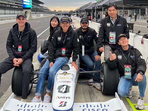 Team KAIST to Race at CES 2022 Autonomous Challenge
Five top university autonomous racing teams will compete in a head-to-head passing competition in Las Vegas
A self-driving racing team from the KAIST Unmanned System Research Group (USRG) advised by Professor Hyunchul Shim will compete at the Autonomous Challenge at the Consumer Electronic Show (CES) on January 7, 2022. The head-to-head, high speed autonomous racecar passing competition at the Las Vegas Motor Speedway will feature the finalists and semifinalists from the Indy Autonomous Challenge in October of this year. Team KAIST qualified as a semifinalist at the Indy Autonomous Challenge and will join four other university teams including the winner of the competition, Technische Universität München.
Team KAIST’s AV-21 vehicle is capable of driving on its own at more than 200km/h will be expected to show a speed of more than 300 km/h at the race.The participating teams are:1. KAIST2. EuroRacing : University of Modena and Reggio Emilia (Italy), University of Pisa (Italy), ETH Zürich (Switzerland), Polish Academy of Sciences (Poland) 3. MIT-PITT-RW, Massachusetts Institute of Technology, University of Pittsburgh, Rochester Institute of Technology, University of Waterloo (Canada)4.PoliMOVE – Politecnico di Milano (Italy), University of Alabama 5.TUM Autonomous Motorsport – Technische Universität München (Germany)
Professor Shim’s team is dedicated to the development and validation of cutting edge technologies for highly autonomous vehicles. In recognition of his pioneering research in unmanned system technologies, Professor Shim was honored with the Grand Prize of the Minister of Science and ICT on December 9.
“We began autonomous vehicle research in 2009 when we signed up for Hyundai Motor Company’s Autonomous Driving Challenge. For this, we developed a complete set of in-house technologies such as low-level vehicle control, perception, localization, and decision making.” In 2019, the team came in third place in the Challenge and they finally won this year.
For years, his team has participated in many unmanned systems challenges at home and abroad, gaining recognition around the world. The team won the inaugural 2016 IROS autonomous drone racing and placed second in the 2018 IROS Autonomous Drone Racing Competition. They also competed in 2017 MBZIRC, ranking fourth in Missions 2 and 3, and fifth in the Grand Challenge.
Most recently, the team won the first round of Lockheed Martin’s Alpha Pilot AI Drone Innovation Challenge. The team is now participating in the DARPA Subterranean Challenge as a member of Team CoSTAR with NASA JPL, MIT, and Caltech.
“We have accumulated plenty of first-hand experience developing autonomous vehicles with the support of domestic companies such as Hyundai Motor Company, Samsung, LG, and NAVER. In 2017, the autonomous vehicle platform “EureCar” that we developed in-house was authorized by the Korean government to lawfully conduct autonomous driving experiment on public roads,” said Professor Shim.
The team has developed various key technologies and algorithms related to unmanned systems that can be categorized into three major components: perception, planning, and control. Considering the characteristics of the algorithms that make up each module, their technology operates using a distributed computing system.
Since 2015, the team has been actively using deep learning algorithms in the form of perception subsystems. Contextual information extracted from multi-modal sensory data gathered via cameras, lidar, radar, GPS, IMU, etc. is forwarded to the planning subsystem. The planning module is responsible for the decision making and planning required for autonomous driving such as lane change determination and trajectory planning, emergency stops, and velocity command generation. The results from the planner are fed into the controller to follow the planned high-level command. The team has also developed and verified the possibility of an end-to-end deep learning based autonomous driving approach that replaces a complex system with one single AI network.
2021.12.17 View 13442
Team KAIST to Race at CES 2022 Autonomous Challenge
Five top university autonomous racing teams will compete in a head-to-head passing competition in Las Vegas
A self-driving racing team from the KAIST Unmanned System Research Group (USRG) advised by Professor Hyunchul Shim will compete at the Autonomous Challenge at the Consumer Electronic Show (CES) on January 7, 2022. The head-to-head, high speed autonomous racecar passing competition at the Las Vegas Motor Speedway will feature the finalists and semifinalists from the Indy Autonomous Challenge in October of this year. Team KAIST qualified as a semifinalist at the Indy Autonomous Challenge and will join four other university teams including the winner of the competition, Technische Universität München.
Team KAIST’s AV-21 vehicle is capable of driving on its own at more than 200km/h will be expected to show a speed of more than 300 km/h at the race.The participating teams are:1. KAIST2. EuroRacing : University of Modena and Reggio Emilia (Italy), University of Pisa (Italy), ETH Zürich (Switzerland), Polish Academy of Sciences (Poland) 3. MIT-PITT-RW, Massachusetts Institute of Technology, University of Pittsburgh, Rochester Institute of Technology, University of Waterloo (Canada)4.PoliMOVE – Politecnico di Milano (Italy), University of Alabama 5.TUM Autonomous Motorsport – Technische Universität München (Germany)
Professor Shim’s team is dedicated to the development and validation of cutting edge technologies for highly autonomous vehicles. In recognition of his pioneering research in unmanned system technologies, Professor Shim was honored with the Grand Prize of the Minister of Science and ICT on December 9.
“We began autonomous vehicle research in 2009 when we signed up for Hyundai Motor Company’s Autonomous Driving Challenge. For this, we developed a complete set of in-house technologies such as low-level vehicle control, perception, localization, and decision making.” In 2019, the team came in third place in the Challenge and they finally won this year.
For years, his team has participated in many unmanned systems challenges at home and abroad, gaining recognition around the world. The team won the inaugural 2016 IROS autonomous drone racing and placed second in the 2018 IROS Autonomous Drone Racing Competition. They also competed in 2017 MBZIRC, ranking fourth in Missions 2 and 3, and fifth in the Grand Challenge.
Most recently, the team won the first round of Lockheed Martin’s Alpha Pilot AI Drone Innovation Challenge. The team is now participating in the DARPA Subterranean Challenge as a member of Team CoSTAR with NASA JPL, MIT, and Caltech.
“We have accumulated plenty of first-hand experience developing autonomous vehicles with the support of domestic companies such as Hyundai Motor Company, Samsung, LG, and NAVER. In 2017, the autonomous vehicle platform “EureCar” that we developed in-house was authorized by the Korean government to lawfully conduct autonomous driving experiment on public roads,” said Professor Shim.
The team has developed various key technologies and algorithms related to unmanned systems that can be categorized into three major components: perception, planning, and control. Considering the characteristics of the algorithms that make up each module, their technology operates using a distributed computing system.
Since 2015, the team has been actively using deep learning algorithms in the form of perception subsystems. Contextual information extracted from multi-modal sensory data gathered via cameras, lidar, radar, GPS, IMU, etc. is forwarded to the planning subsystem. The planning module is responsible for the decision making and planning required for autonomous driving such as lane change determination and trajectory planning, emergency stops, and velocity command generation. The results from the planner are fed into the controller to follow the planned high-level command. The team has also developed and verified the possibility of an end-to-end deep learning based autonomous driving approach that replaces a complex system with one single AI network.
2021.12.17 View 13442 -
 Scientists Develop Wireless Networks that Allow Brain Circuits to Be Controlled Remotely through the Internet
Wireless implantable devices and IoT could manipulate the brains of animals from anywhere around the world due to their minimalistic hardware, low setup cost, ease of use, and customizable versatility
A new study shows that researchers can remotely control the brain circuits of numerous animals simultaneously and independently through the internet. The scientists believe this newly developed technology can speed up brain research and various neuroscience studies to uncover basic brain functions as well as the underpinnings of various neuropsychiatric and neurological disorders.
A multidisciplinary team of researchers at KAIST, Washington University in St. Louis, and the University of Colorado, Boulder, created a wireless ecosystem with its own wireless implantable devices and Internet of Things (IoT) infrastructure to enable high-throughput neuroscience experiments over the internet. This innovative technology could enable scientists to manipulate the brains of animals from anywhere around the world. The study was published in the journal Nature Biomedical Engineering on November 25
“This novel technology is highly versatile and adaptive. It can remotely control numerous neural implants and laboratory tools in real-time or in a scheduled way without direct human interactions,” said Professor Jae-Woong Jeong of the School of Electrical Engineering at KAIST and a senior author of the study. “These wireless neural devices and equipment integrated with IoT technology have enormous potential for science and medicine.”
The wireless ecosystem only requires a mini-computer that can be purchased for under $45, which connects to the internet and communicates with wireless multifunctional brain probes or other types of conventional laboratory equipment using IoT control modules. By optimally integrating the versatility and modular construction of both unique IoT hardware and software within a single ecosystem, this wireless technology offers new applications that have not been demonstrated before by a single standalone technology. This includes, but is not limited to minimalistic hardware, global remote access, selective and scheduled experiments, customizable automation, and high-throughput scalability.
“As long as researchers have internet access, they are able to trigger, customize, stop, validate, and store the outcomes of large experiments at any time and from anywhere in the world. They can remotely perform large-scale neuroscience experiments in animals deployed in multiple countries,” said one of the lead authors, Dr. Raza Qazi, a researcher with KAIST and the University of Colorado, Boulder. “The low cost of this system allows it to be easily adopted and can further fuel innovation across many laboratories,” Dr. Qazi added.
One of the significant advantages of this IoT neurotechnology is its ability to be mass deployed across the globe due to its minimalistic hardware, low setup cost, ease of use, and customizable versatility. Scientists across the world can quickly implement this technology within their existing laboratories with minimal budget concerns to achieve globally remote access, scalable experimental automation, or both, thus potentially reducing the time needed to unravel various neuroscientific challenges such as those associated with intractable neurological conditions.
Another senior author on the study, Professor Jordan McCall from the Department of Anesthesiology and Center for Clinical Pharmacology at Washington University in St. Louis, said this technology has the potential to change how basic neuroscience studies are performed. “One of the biggest limitations when trying to understand how the mammalian brain works is that we have to study these functions in unnatural conditions. This technology brings us one step closer to performing important studies without direct human interaction with the study subjects.”
The ability to remotely schedule experiments moves toward automating these types of experiments. Dr. Kyle Parker, an instructor at Washington University in St. Louis and another lead author on the study added, “This experimental automation can potentially help us reduce the number of animals used in biomedical research by reducing the variability introduced by various experimenters. This is especially important given our moral imperative to seek research designs that enable this reduction.”
The researchers believe this wireless technology may open new opportunities for many applications including brain research, pharmaceuticals, and telemedicine to treat diseases in the brain and other organs remotely. This remote automation technology could become even more valuable when many labs need to shut down, such as during the height of the COVID-19 pandemic.
This work was supported by grants from the KAIST Global Singularity Research Program, the National Research Foundation of Korea, the United States National Institute of Health, and Oak Ridge Associated Universities.
-PublicationRaza Qazi, Kyle Parker, Choong Yeon Kim, Jordan McCall, Jae-Woong Jeong et al. “Scalable and modular wireless-network infrastructure for large-scale behavioral neuroscience,” Nature Biomedical Engineering, November 25 2021 (doi.org/10.1038/s41551-021-00814-w)
-ProfileProfessor Jae-Woong JeongBio-Integrated Electronics and Systems LabSchool of Electrical EngineeringKAIST
2021.11.29 View 18270
Scientists Develop Wireless Networks that Allow Brain Circuits to Be Controlled Remotely through the Internet
Wireless implantable devices and IoT could manipulate the brains of animals from anywhere around the world due to their minimalistic hardware, low setup cost, ease of use, and customizable versatility
A new study shows that researchers can remotely control the brain circuits of numerous animals simultaneously and independently through the internet. The scientists believe this newly developed technology can speed up brain research and various neuroscience studies to uncover basic brain functions as well as the underpinnings of various neuropsychiatric and neurological disorders.
A multidisciplinary team of researchers at KAIST, Washington University in St. Louis, and the University of Colorado, Boulder, created a wireless ecosystem with its own wireless implantable devices and Internet of Things (IoT) infrastructure to enable high-throughput neuroscience experiments over the internet. This innovative technology could enable scientists to manipulate the brains of animals from anywhere around the world. The study was published in the journal Nature Biomedical Engineering on November 25
“This novel technology is highly versatile and adaptive. It can remotely control numerous neural implants and laboratory tools in real-time or in a scheduled way without direct human interactions,” said Professor Jae-Woong Jeong of the School of Electrical Engineering at KAIST and a senior author of the study. “These wireless neural devices and equipment integrated with IoT technology have enormous potential for science and medicine.”
The wireless ecosystem only requires a mini-computer that can be purchased for under $45, which connects to the internet and communicates with wireless multifunctional brain probes or other types of conventional laboratory equipment using IoT control modules. By optimally integrating the versatility and modular construction of both unique IoT hardware and software within a single ecosystem, this wireless technology offers new applications that have not been demonstrated before by a single standalone technology. This includes, but is not limited to minimalistic hardware, global remote access, selective and scheduled experiments, customizable automation, and high-throughput scalability.
“As long as researchers have internet access, they are able to trigger, customize, stop, validate, and store the outcomes of large experiments at any time and from anywhere in the world. They can remotely perform large-scale neuroscience experiments in animals deployed in multiple countries,” said one of the lead authors, Dr. Raza Qazi, a researcher with KAIST and the University of Colorado, Boulder. “The low cost of this system allows it to be easily adopted and can further fuel innovation across many laboratories,” Dr. Qazi added.
One of the significant advantages of this IoT neurotechnology is its ability to be mass deployed across the globe due to its minimalistic hardware, low setup cost, ease of use, and customizable versatility. Scientists across the world can quickly implement this technology within their existing laboratories with minimal budget concerns to achieve globally remote access, scalable experimental automation, or both, thus potentially reducing the time needed to unravel various neuroscientific challenges such as those associated with intractable neurological conditions.
Another senior author on the study, Professor Jordan McCall from the Department of Anesthesiology and Center for Clinical Pharmacology at Washington University in St. Louis, said this technology has the potential to change how basic neuroscience studies are performed. “One of the biggest limitations when trying to understand how the mammalian brain works is that we have to study these functions in unnatural conditions. This technology brings us one step closer to performing important studies without direct human interaction with the study subjects.”
The ability to remotely schedule experiments moves toward automating these types of experiments. Dr. Kyle Parker, an instructor at Washington University in St. Louis and another lead author on the study added, “This experimental automation can potentially help us reduce the number of animals used in biomedical research by reducing the variability introduced by various experimenters. This is especially important given our moral imperative to seek research designs that enable this reduction.”
The researchers believe this wireless technology may open new opportunities for many applications including brain research, pharmaceuticals, and telemedicine to treat diseases in the brain and other organs remotely. This remote automation technology could become even more valuable when many labs need to shut down, such as during the height of the COVID-19 pandemic.
This work was supported by grants from the KAIST Global Singularity Research Program, the National Research Foundation of Korea, the United States National Institute of Health, and Oak Ridge Associated Universities.
-PublicationRaza Qazi, Kyle Parker, Choong Yeon Kim, Jordan McCall, Jae-Woong Jeong et al. “Scalable and modular wireless-network infrastructure for large-scale behavioral neuroscience,” Nature Biomedical Engineering, November 25 2021 (doi.org/10.1038/s41551-021-00814-w)
-ProfileProfessor Jae-Woong JeongBio-Integrated Electronics and Systems LabSchool of Electrical EngineeringKAIST
2021.11.29 View 18270 -
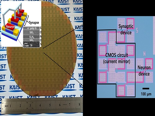 Brain-Inspired Highly Scalable Neuromorphic Hardware Presented
Neurons and synapses based on single transistor can dramatically reduce the hardware cost and accelerate the commercialization of neuromorphic hardware
KAIST researchers fabricated a brain-inspired highly scalable neuromorphic hardware by co-integrating single transistor neurons and synapses. Using standard silicon complementary metal-oxide-semiconductor (CMOS) technology, the neuromorphic hardware is expected to reduce chip cost and simplify fabrication procedures.
The research team led by Yang-Kyu Choi and Sung-Yool Choi produced a neurons and synapses based on single transistor for highly scalable neuromorphic hardware and showed the ability to recognize text and face images. This research was featured in Science Advances on August 4.
Neuromorphic hardware has attracted a great deal of attention because of its artificial intelligence functions, but consuming ultra-low power of less than 20 watts by mimicking the human brain. To make neuromorphic hardware work, a neuron that generates a spike when integrating a certain signal, and a synapse remembering the connection between two neurons are necessary, just like the biological brain. However, since neurons and synapses constructed on digital or analog circuits occupy a large space, there is a limit in terms of hardware efficiency and costs. Since the human brain consists of about 1011 neurons and 1014 synapses, it is necessary to improve the hardware cost in order to apply it to mobile and IoT devices.
To solve the problem, the research team mimicked the behavior of biological neurons and synapses with a single transistor, and co-integrated them onto an 8-inch wafer. The manufactured neuromorphic transistors have the same structure as the transistors for memory and logic that are currently mass-produced. In addition, the neuromorphic transistors proved for the first time that they can be implemented with a ‘Janus structure’ that functions as both neuron and synapse, just like coins have heads and tails.
Professor Yang-Kyu Choi said that this work can dramatically reduce the hardware cost by replacing the neurons and synapses that were based on complex digital and analog circuits with a single transistor. "We have demonstrated that neurons and synapses can be implemented using a single transistor," said Joon-Kyu Han, the first author. "By co-integrating single transistor neurons and synapses on the same wafer using a standard CMOS process, the hardware cost of the neuromorphic hardware has been improved, which will accelerate the commercialization of neuromorphic hardware,” Han added.This research was supported by the National Research Foundation (NRF) and IC Design Education Center (IDEC).
-PublicationJoon-Kyu Han, Sung-Yool Choi, Yang-Kyu Choi, et al.“Cointegration of single-transistor neurons and synapses by nanoscale CMOS fabrication for highly scalable neuromorphic hardware,” Science Advances (DOI: 10.1126/sciadv.abg8836)
-ProfileProfessor Yang-Kyu ChoiNano-Oriented Bio-Electronics Labhttps://sites.google.com/view/nobelab/
School of Electrical EngineeringKAIST
Professor Sung-Yool ChoiMolecular and Nano Device Laboratoryhttps://www.mndl.kaist.ac.kr/
School of Electrical EngineeringKAIST
2021.08.05 View 13358
Brain-Inspired Highly Scalable Neuromorphic Hardware Presented
Neurons and synapses based on single transistor can dramatically reduce the hardware cost and accelerate the commercialization of neuromorphic hardware
KAIST researchers fabricated a brain-inspired highly scalable neuromorphic hardware by co-integrating single transistor neurons and synapses. Using standard silicon complementary metal-oxide-semiconductor (CMOS) technology, the neuromorphic hardware is expected to reduce chip cost and simplify fabrication procedures.
The research team led by Yang-Kyu Choi and Sung-Yool Choi produced a neurons and synapses based on single transistor for highly scalable neuromorphic hardware and showed the ability to recognize text and face images. This research was featured in Science Advances on August 4.
Neuromorphic hardware has attracted a great deal of attention because of its artificial intelligence functions, but consuming ultra-low power of less than 20 watts by mimicking the human brain. To make neuromorphic hardware work, a neuron that generates a spike when integrating a certain signal, and a synapse remembering the connection between two neurons are necessary, just like the biological brain. However, since neurons and synapses constructed on digital or analog circuits occupy a large space, there is a limit in terms of hardware efficiency and costs. Since the human brain consists of about 1011 neurons and 1014 synapses, it is necessary to improve the hardware cost in order to apply it to mobile and IoT devices.
To solve the problem, the research team mimicked the behavior of biological neurons and synapses with a single transistor, and co-integrated them onto an 8-inch wafer. The manufactured neuromorphic transistors have the same structure as the transistors for memory and logic that are currently mass-produced. In addition, the neuromorphic transistors proved for the first time that they can be implemented with a ‘Janus structure’ that functions as both neuron and synapse, just like coins have heads and tails.
Professor Yang-Kyu Choi said that this work can dramatically reduce the hardware cost by replacing the neurons and synapses that were based on complex digital and analog circuits with a single transistor. "We have demonstrated that neurons and synapses can be implemented using a single transistor," said Joon-Kyu Han, the first author. "By co-integrating single transistor neurons and synapses on the same wafer using a standard CMOS process, the hardware cost of the neuromorphic hardware has been improved, which will accelerate the commercialization of neuromorphic hardware,” Han added.This research was supported by the National Research Foundation (NRF) and IC Design Education Center (IDEC).
-PublicationJoon-Kyu Han, Sung-Yool Choi, Yang-Kyu Choi, et al.“Cointegration of single-transistor neurons and synapses by nanoscale CMOS fabrication for highly scalable neuromorphic hardware,” Science Advances (DOI: 10.1126/sciadv.abg8836)
-ProfileProfessor Yang-Kyu ChoiNano-Oriented Bio-Electronics Labhttps://sites.google.com/view/nobelab/
School of Electrical EngineeringKAIST
Professor Sung-Yool ChoiMolecular and Nano Device Laboratoryhttps://www.mndl.kaist.ac.kr/
School of Electrical EngineeringKAIST
2021.08.05 View 13358 -
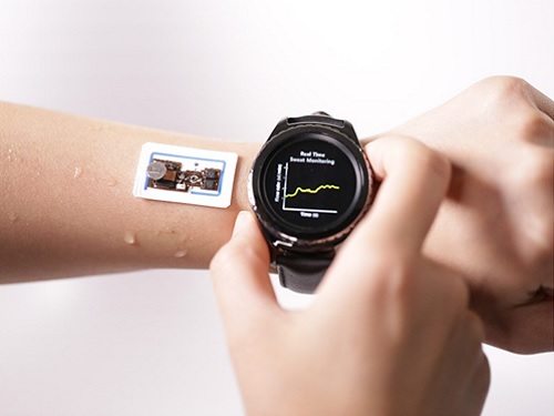 Wearable Device to Monitor Sweat in Real Time
An on-skin platform for the wireless monitoring of flow rate, cumulative loss, and temperature of sweat in real time
An electronic patch can monitor your sweating and check your health status. Even more, the soft microfluidic device that adheres to the surface of the skin, captures, stores, and performs biomarker analysis of sweat as it is released through the eccrine glands.
This wearable and wireless electronic device developed by Professor Kyeongha Kwon and her collaborators is a digital and wireless platform that could help track the so-called ‘filling process’ of sweat without having to visually examine the device. The platform was integrated with microfluidic systems to analyze the sweat’s components.
To monitor the sweat release rate in real time, the researchers created a ‘thermal flow sensing module.’ They designed a sophisticated microfluidic channel to allow the collected sweat to flow through a narrow passage and a heat source was placed on the outer surface of the channel to induce a heat exchange between the sweat and the heated channel.
As a result, the researchers could develop a wireless electronic patch that can measure the temperature difference in a specific location upstream and downstream of the heat source with an electronic circuit and convert it into a digital signal to measure the sweat release rate in real time. The patch accurately measured the perspiration rate in the range of 0-5 microliters/minute (μl/min), which was considered physiologically significant. The sensor can measure the flow of sweat directly and then use the information it collected to quantify total sweat loss. Moreover, the device features advanced microfluidic systems and colorimetric chemical reagents to gather pH measurements and determine the concentration of chloride, creatinine, and glucose in a user's sweat.
Professor Kwon said that these indicators could be used to diagnose various diseases related with sweating such as cystic fibrosis, diabetes, kidney dysfunction, and metabolic alkalosis. “As the sweat flowing in the microfluidic channel is completely separated from the electronic circuit, the new patch overcame the shortcomings of existing flow rate measuring devices, which were vulnerable to corrosion and aging,” she explained.
The patch can be easily attached to the skin with flexible circuit board printing technology and silicone sealing technology. It has an additional sensor that detects changes in skin temperature. Using a smartphone app, a user can check the data measured by the wearable patch in real time.
Professor Kwon added, “This patch can be widely used for personal hydration strategies, the detection of dehydration symptoms, and other health management purposes. It can also be used in a systematic drug delivery system, such as for measuring the blood flow rate in blood vessels near the skin’s surface or measuring a drug’s release rate in real time to calculate the exact dosage.”
-PublicationKyeongha Kwon, Jong Uk Kim, John A. Rogers, et al. “An on-skin platform for wireless monitoring of flow rate, cumulative loss and temperature of sweat in real time.” Nature Electronics (doi.org/10.1038/s41928-021-00556-2)
-ProfileProfessor Kyeongha KwonSchool of Electrical EngineeringKAIST
2021.06.25 View 13034
Wearable Device to Monitor Sweat in Real Time
An on-skin platform for the wireless monitoring of flow rate, cumulative loss, and temperature of sweat in real time
An electronic patch can monitor your sweating and check your health status. Even more, the soft microfluidic device that adheres to the surface of the skin, captures, stores, and performs biomarker analysis of sweat as it is released through the eccrine glands.
This wearable and wireless electronic device developed by Professor Kyeongha Kwon and her collaborators is a digital and wireless platform that could help track the so-called ‘filling process’ of sweat without having to visually examine the device. The platform was integrated with microfluidic systems to analyze the sweat’s components.
To monitor the sweat release rate in real time, the researchers created a ‘thermal flow sensing module.’ They designed a sophisticated microfluidic channel to allow the collected sweat to flow through a narrow passage and a heat source was placed on the outer surface of the channel to induce a heat exchange between the sweat and the heated channel.
As a result, the researchers could develop a wireless electronic patch that can measure the temperature difference in a specific location upstream and downstream of the heat source with an electronic circuit and convert it into a digital signal to measure the sweat release rate in real time. The patch accurately measured the perspiration rate in the range of 0-5 microliters/minute (μl/min), which was considered physiologically significant. The sensor can measure the flow of sweat directly and then use the information it collected to quantify total sweat loss. Moreover, the device features advanced microfluidic systems and colorimetric chemical reagents to gather pH measurements and determine the concentration of chloride, creatinine, and glucose in a user's sweat.
Professor Kwon said that these indicators could be used to diagnose various diseases related with sweating such as cystic fibrosis, diabetes, kidney dysfunction, and metabolic alkalosis. “As the sweat flowing in the microfluidic channel is completely separated from the electronic circuit, the new patch overcame the shortcomings of existing flow rate measuring devices, which were vulnerable to corrosion and aging,” she explained.
The patch can be easily attached to the skin with flexible circuit board printing technology and silicone sealing technology. It has an additional sensor that detects changes in skin temperature. Using a smartphone app, a user can check the data measured by the wearable patch in real time.
Professor Kwon added, “This patch can be widely used for personal hydration strategies, the detection of dehydration symptoms, and other health management purposes. It can also be used in a systematic drug delivery system, such as for measuring the blood flow rate in blood vessels near the skin’s surface or measuring a drug’s release rate in real time to calculate the exact dosage.”
-PublicationKyeongha Kwon, Jong Uk Kim, John A. Rogers, et al. “An on-skin platform for wireless monitoring of flow rate, cumulative loss and temperature of sweat in real time.” Nature Electronics (doi.org/10.1038/s41928-021-00556-2)
-ProfileProfessor Kyeongha KwonSchool of Electrical EngineeringKAIST
2021.06.25 View 13034 -
 Observing Individual Atoms in 3D Nanomaterials and Their Surfaces
Atoms are the basic building blocks for all materials. To tailor functional properties, it is essential to accurately determine their atomic structures. KAIST researchers observed the 3D atomic structure of a nanoparticle at the atom level via neural network-assisted atomic electron tomography.
Using a platinum nanoparticle as a model system, a research team led by Professor Yongsoo Yang demonstrated that an atomicity-based deep learning approach can reliably identify the 3D surface atomic structure with a precision of 15 picometers (only about 1/3 of a hydrogen atom’s radius). The atomic displacement, strain, and facet analysis revealed that the surface atomic structure and strain are related to both the shape of the nanoparticle and the particle-substrate interface.
Combined with quantum mechanical calculations such as density functional theory, the ability to precisely identify surface atomic structure will serve as a powerful key for understanding catalytic performance and oxidation effect.
“We solved the problem of determining the 3D surface atomic structure of nanomaterials in a reliable manner. It has been difficult to accurately measure the surface atomic structures due to the ‘missing wedge problem’ in electron tomography, which arises from geometrical limitations, allowing only part of a full tomographic angular range to be measured. We resolved the problem using a deep learning-based approach,” explained Professor Yang.
The missing wedge problem results in elongation and ringing artifacts, negatively affecting the accuracy of the atomic structure determined from the tomogram, especially for identifying the surface structures. The missing wedge problem has been the main roadblock for the precise determination of the 3D surface atomic structures of nanomaterials.
The team used atomic electron tomography (AET), which is basically a very high-resolution CT scan for nanomaterials using transmission electron microscopes. AET allows individual atom level 3D atomic structural determination.
“The main idea behind this deep learning-based approach is atomicity—the fact that all matter is composed of atoms. This means that true atomic resolution electron tomogram should only contain sharp 3D atomic potentials convolved with the electron beam profile,” said Professor Yang.
“A deep neural network can be trained using simulated tomograms that suffer from missing wedges as inputs, and the ground truth 3D atomic volumes as targets. The trained deep learning network effectively augments the imperfect tomograms and removes the artifacts resulting from the missing wedge problem.”
The precision of 3D atomic structure can be enhanced by nearly 70% by applying the deep learning-based augmentation. The accuracy of surface atom identification was also significantly improved.
Structure-property relationships of functional nanomaterials, especially the ones that strongly depend on the surface structures, such as catalytic properties for fuel-cell applications, can now be revealed at one of the most fundamental scales: the atomic scale.
Professor Yang concluded, “We would like to fully map out the 3D atomic structure with higher precision and better elemental specificity. And not being limited to atomic structures, we aim to measure the physical, chemical, and functional properties of nanomaterials at the 3D atomic scale by further advancing electron tomography techniques.”
This research, reported at Nature Communications, was funded by the National Research Foundation of Korea and the KAIST Global Singularity Research M3I3 Project.
-Publication
Juhyeok Lee, Chaehwa Jeong & Yongsoo Yang
“Single-atom level determination of 3-dimensional surface atomic structure via neural network-assisted atomic electron tomography”
Nature Communications
-Profile
Professor Yongsoo Yang
Department of Physics
Multi-Dimensional Atomic Imaging Lab (MDAIL)
http://mdail.kaist.ac.kr
KAIST
2021.05.12 View 14798
Observing Individual Atoms in 3D Nanomaterials and Their Surfaces
Atoms are the basic building blocks for all materials. To tailor functional properties, it is essential to accurately determine their atomic structures. KAIST researchers observed the 3D atomic structure of a nanoparticle at the atom level via neural network-assisted atomic electron tomography.
Using a platinum nanoparticle as a model system, a research team led by Professor Yongsoo Yang demonstrated that an atomicity-based deep learning approach can reliably identify the 3D surface atomic structure with a precision of 15 picometers (only about 1/3 of a hydrogen atom’s radius). The atomic displacement, strain, and facet analysis revealed that the surface atomic structure and strain are related to both the shape of the nanoparticle and the particle-substrate interface.
Combined with quantum mechanical calculations such as density functional theory, the ability to precisely identify surface atomic structure will serve as a powerful key for understanding catalytic performance and oxidation effect.
“We solved the problem of determining the 3D surface atomic structure of nanomaterials in a reliable manner. It has been difficult to accurately measure the surface atomic structures due to the ‘missing wedge problem’ in electron tomography, which arises from geometrical limitations, allowing only part of a full tomographic angular range to be measured. We resolved the problem using a deep learning-based approach,” explained Professor Yang.
The missing wedge problem results in elongation and ringing artifacts, negatively affecting the accuracy of the atomic structure determined from the tomogram, especially for identifying the surface structures. The missing wedge problem has been the main roadblock for the precise determination of the 3D surface atomic structures of nanomaterials.
The team used atomic electron tomography (AET), which is basically a very high-resolution CT scan for nanomaterials using transmission electron microscopes. AET allows individual atom level 3D atomic structural determination.
“The main idea behind this deep learning-based approach is atomicity—the fact that all matter is composed of atoms. This means that true atomic resolution electron tomogram should only contain sharp 3D atomic potentials convolved with the electron beam profile,” said Professor Yang.
“A deep neural network can be trained using simulated tomograms that suffer from missing wedges as inputs, and the ground truth 3D atomic volumes as targets. The trained deep learning network effectively augments the imperfect tomograms and removes the artifacts resulting from the missing wedge problem.”
The precision of 3D atomic structure can be enhanced by nearly 70% by applying the deep learning-based augmentation. The accuracy of surface atom identification was also significantly improved.
Structure-property relationships of functional nanomaterials, especially the ones that strongly depend on the surface structures, such as catalytic properties for fuel-cell applications, can now be revealed at one of the most fundamental scales: the atomic scale.
Professor Yang concluded, “We would like to fully map out the 3D atomic structure with higher precision and better elemental specificity. And not being limited to atomic structures, we aim to measure the physical, chemical, and functional properties of nanomaterials at the 3D atomic scale by further advancing electron tomography techniques.”
This research, reported at Nature Communications, was funded by the National Research Foundation of Korea and the KAIST Global Singularity Research M3I3 Project.
-Publication
Juhyeok Lee, Chaehwa Jeong & Yongsoo Yang
“Single-atom level determination of 3-dimensional surface atomic structure via neural network-assisted atomic electron tomography”
Nature Communications
-Profile
Professor Yongsoo Yang
Department of Physics
Multi-Dimensional Atomic Imaging Lab (MDAIL)
http://mdail.kaist.ac.kr
KAIST
2021.05.12 View 14798 -
 Acoustic Graphene Plasmons Study Paves Way for Optoelectronic Applications
- The first images of mid-infrared optical waves compressed 1,000 times captured using a highly sensitive scattering-type scanning near-field optical microscope. -
KAIST researchers and their collaborators at home and abroad have successfully demonstrated a new methodology for direct near-field optical imaging of acoustic graphene plasmon fields. This strategy will provide a breakthrough for the practical applications of acoustic graphene plasmon platforms in next-generation, high-performance, graphene-based optoelectronic devices with enhanced light-matter interactions and lower propagation loss.
It was recently demonstrated that ‘graphene plasmons’ – collective oscillations of free electrons in graphene coupled to electromagnetic waves of light – can be used to trap and compress optical waves inside a very thin dielectric layer separating graphene from a metallic sheet. In such a configuration, graphene’s conduction electrons are “reflected” in the metal, so when the light waves “push” the electrons in graphene, their image charges in metal also start to oscillate. This new type of collective electronic oscillation mode is called ‘acoustic graphene plasmon (AGP)’.
The existence of AGP could previously be observed only via indirect methods such as far-field infrared spectroscopy and photocurrent mapping. This indirect observation was the price that researchers had to pay for the strong compression of optical waves inside nanometer-thin structures. It was believed that the intensity of electromagnetic fields outside the device was insufficient for direct near-field optical imaging of AGP.
Challenged by these limitations, three research groups combined their efforts to bring together a unique experimental technique using advanced nanofabrication methods. Their findings were published in Nature Communications on February 19.
A KAIST research team led by Professor Min Seok Jang from the School of Electrical Engineering used a highly sensitive scattering-type scanning near-field optical microscope (s-SNOM) to directly measure the optical fields of the AGP waves propagating in a nanometer-thin waveguide, visualizing thousand-fold compression of mid-infrared light for the first time.
Professor Jang and a post-doc researcher in his group, Sergey G. Menabde, successfully obtained direct images of AGP waves by taking advantage of their rapidly decaying yet always present electric field above graphene. They showed that AGPs are detectable even when most of their energy is flowing inside the dielectric below the graphene.
This became possible due to the ultra-smooth surfaces inside the nano-waveguides where plasmonic waves can propagate at longer distances. The AGP mode probed by the researchers was up to 2.3 times more confined and exhibited a 1.4 times higher figure of merit in terms of the normalized propagation length compared to the graphene surface plasmon under similar conditions.
These ultra-smooth nanostructures of the waveguides used in the experiment were created using a template-stripping method by Professor Sang-Hyun Oh and a post-doc researcher, In-Ho Lee, from the Department of Electrical and Computer Engineering at the University of Minnesota.
Professor Young Hee Lee and his researchers at the Center for Integrated Nanostructure Physics (CINAP) of the Institute of Basic Science (IBS) at Sungkyunkwan University synthesized the graphene with a monocrystalline structure, and this high-quality, large-area graphene enabled low-loss plasmonic propagation.
The chemical and physical properties of many important organic molecules can be detected and evaluated by their absorption signatures in the mid-infrared spectrum. However, conventional detection methods require a large number of molecules for successful detection, whereas the ultra-compressed AGP fields can provide strong light-matter interactions at the microscopic level, thus significantly improving the detection sensitivity down to a single molecule.
Furthermore, the study conducted by Professor Jang and the team demonstrated that the mid-infrared AGPs are inherently less sensitive to losses in graphene due to their fields being mostly confined within the dielectric. The research team’s reported results suggest that AGPs could become a promising platform for electrically tunable graphene-based optoelectronic devices that typically suffer from higher absorption rates in graphene such as metasurfaces, optical switches, photovoltaics, and other optoelectronic applications operating at infrared frequencies.
Professor Jang said, “Our research revealed that the ultra-compressed electromagnetic fields of acoustic graphene plasmons can be directly accessed through near-field optical microscopy methods. I hope this realization will motivate other researchers to apply AGPs to various problems where strong light-matter interactions and lower propagation loss are needed.”
This research was primarily funded by the Samsung Research Funding & Incubation Center of Samsung Electronics. The National Research Foundation of Korea (NRF), the U.S. National Science Foundation (NSF), Samsung Global Research Outreach (GRO) Program, and Institute for Basic Science of Korea (IBS) also supported the work.
Publication:
Menabde, S. G., et al. (2021) Real-space imaging of acoustic plasmons in large-area graphene grown by chemical vapor deposition. Nature Communications 12, Article No. 938. Available online at https://doi.org/10.1038/s41467-021-21193-5
Profile:
Min Seok Jang, MS, PhD
Associate Professorjang.minseok@kaist.ac.krhttp://jlab.kaist.ac.kr/
Min Seok Jang Research GroupSchool of Electrical Engineering
http://kaist.ac.kr/en/Korea Advanced Institute of Science and Technology (KAIST)Daejeon, Republic of Korea
(END)
2021.03.16 View 16856
Acoustic Graphene Plasmons Study Paves Way for Optoelectronic Applications
- The first images of mid-infrared optical waves compressed 1,000 times captured using a highly sensitive scattering-type scanning near-field optical microscope. -
KAIST researchers and their collaborators at home and abroad have successfully demonstrated a new methodology for direct near-field optical imaging of acoustic graphene plasmon fields. This strategy will provide a breakthrough for the practical applications of acoustic graphene plasmon platforms in next-generation, high-performance, graphene-based optoelectronic devices with enhanced light-matter interactions and lower propagation loss.
It was recently demonstrated that ‘graphene plasmons’ – collective oscillations of free electrons in graphene coupled to electromagnetic waves of light – can be used to trap and compress optical waves inside a very thin dielectric layer separating graphene from a metallic sheet. In such a configuration, graphene’s conduction electrons are “reflected” in the metal, so when the light waves “push” the electrons in graphene, their image charges in metal also start to oscillate. This new type of collective electronic oscillation mode is called ‘acoustic graphene plasmon (AGP)’.
The existence of AGP could previously be observed only via indirect methods such as far-field infrared spectroscopy and photocurrent mapping. This indirect observation was the price that researchers had to pay for the strong compression of optical waves inside nanometer-thin structures. It was believed that the intensity of electromagnetic fields outside the device was insufficient for direct near-field optical imaging of AGP.
Challenged by these limitations, three research groups combined their efforts to bring together a unique experimental technique using advanced nanofabrication methods. Their findings were published in Nature Communications on February 19.
A KAIST research team led by Professor Min Seok Jang from the School of Electrical Engineering used a highly sensitive scattering-type scanning near-field optical microscope (s-SNOM) to directly measure the optical fields of the AGP waves propagating in a nanometer-thin waveguide, visualizing thousand-fold compression of mid-infrared light for the first time.
Professor Jang and a post-doc researcher in his group, Sergey G. Menabde, successfully obtained direct images of AGP waves by taking advantage of their rapidly decaying yet always present electric field above graphene. They showed that AGPs are detectable even when most of their energy is flowing inside the dielectric below the graphene.
This became possible due to the ultra-smooth surfaces inside the nano-waveguides where plasmonic waves can propagate at longer distances. The AGP mode probed by the researchers was up to 2.3 times more confined and exhibited a 1.4 times higher figure of merit in terms of the normalized propagation length compared to the graphene surface plasmon under similar conditions.
These ultra-smooth nanostructures of the waveguides used in the experiment were created using a template-stripping method by Professor Sang-Hyun Oh and a post-doc researcher, In-Ho Lee, from the Department of Electrical and Computer Engineering at the University of Minnesota.
Professor Young Hee Lee and his researchers at the Center for Integrated Nanostructure Physics (CINAP) of the Institute of Basic Science (IBS) at Sungkyunkwan University synthesized the graphene with a monocrystalline structure, and this high-quality, large-area graphene enabled low-loss plasmonic propagation.
The chemical and physical properties of many important organic molecules can be detected and evaluated by their absorption signatures in the mid-infrared spectrum. However, conventional detection methods require a large number of molecules for successful detection, whereas the ultra-compressed AGP fields can provide strong light-matter interactions at the microscopic level, thus significantly improving the detection sensitivity down to a single molecule.
Furthermore, the study conducted by Professor Jang and the team demonstrated that the mid-infrared AGPs are inherently less sensitive to losses in graphene due to their fields being mostly confined within the dielectric. The research team’s reported results suggest that AGPs could become a promising platform for electrically tunable graphene-based optoelectronic devices that typically suffer from higher absorption rates in graphene such as metasurfaces, optical switches, photovoltaics, and other optoelectronic applications operating at infrared frequencies.
Professor Jang said, “Our research revealed that the ultra-compressed electromagnetic fields of acoustic graphene plasmons can be directly accessed through near-field optical microscopy methods. I hope this realization will motivate other researchers to apply AGPs to various problems where strong light-matter interactions and lower propagation loss are needed.”
This research was primarily funded by the Samsung Research Funding & Incubation Center of Samsung Electronics. The National Research Foundation of Korea (NRF), the U.S. National Science Foundation (NSF), Samsung Global Research Outreach (GRO) Program, and Institute for Basic Science of Korea (IBS) also supported the work.
Publication:
Menabde, S. G., et al. (2021) Real-space imaging of acoustic plasmons in large-area graphene grown by chemical vapor deposition. Nature Communications 12, Article No. 938. Available online at https://doi.org/10.1038/s41467-021-21193-5
Profile:
Min Seok Jang, MS, PhD
Associate Professorjang.minseok@kaist.ac.krhttp://jlab.kaist.ac.kr/
Min Seok Jang Research GroupSchool of Electrical Engineering
http://kaist.ac.kr/en/Korea Advanced Institute of Science and Technology (KAIST)Daejeon, Republic of Korea
(END)
2021.03.16 View 16856 -
 Attachable Skin Monitors that Wick the Sweat Away
- A silicone membrane for wearable devices is more comfortable and breathable thanks to better-sized pores made with the help of citric acid crystals. -
A new preparation technique fabricates thin, silicone-based patches that rapidly wick water away from the skin. The technique could reduce the redness and itching caused by wearable biosensors that trap sweat beneath them. The technique was developed by bioengineer and professor Young-Ho Cho and his colleagues at KAIST and reported in the journal Scientific Reports last month.
“Wearable bioelectronics are becoming more attractive for the day-to-day monitoring of biological compounds found in sweat, like hormones or glucose, as well as body temperature, heart rate, and energy expenditure,” Professor Cho explained. “But currently available materials can cause skin irritation, so scientists are looking for ways to improve them,” he added.
Attachable biosensors often use a silicone-based compound called polydimethylsiloxane (PDMS), as it has a relatively high water vapour transmission rate compared to other materials. Still, this rate is only two-thirds that of skin’s water evaporation rate, meaning sweat still gets trapped underneath it.
Current fabrication approaches mix PDMS with beads or solutes, such as sugars or salts, and then remove them to leave pores in their place. Another technique uses gas to form pores in the material. Each technique has its disadvantages, from being expensive and complex to leaving pores of different sizes.
A team of researchers led by Professor Cho from the KAIST Department of Bio and Brain Engineering was able to form small, uniform pores by crystallizing citric acid in PDMS and then removing the crystals using ethanol. The approach is significantly cheaper than using beads, and leads to 93.2% smaller and 425% more uniformly-sized pores compared to using sugar. Importantly, the membrane transmits water vapour 2.2 times faster than human skin.
The team tested their membrane on human skin for seven days and found that it caused only minor redness and no itching, whereas a non-porous PDMS membrane did.
Professor Cho said, “Our method could be used to fabricate porous PDMS membranes for skin-attachable devices used for daily monitoring of physiological signals.”
“We next plan to modify our membrane so it can be more readily attached to and removed from skin,” he added.
This work was supported by the Ministry of Trade, Industry and Energy (MOTIE) of Korea under the Alchemist Project.
Image description:
Smaller, more uniformly-sized pores are made in the PDMS membrane by mixing PDMS, toluene, citric acid, and ethanol. Toluene dilutes PDMS so it can easily mix with the other two constituents. Toluene and ethanol are then evaporated, which causes the citric acid to crystallize within the PDMS material. The mixture is placed in a mould where it solidifies into a thin film. The crystals are then removed using ethanol, leaving pores in their place.
Image credit:
Professor Young-Ho Cho, KAIST
Image usage restrictions:
News organizations may use or redistribute this image, with proper attribution, as part of news coverage of this paper only.
Publication:
Yoon, S, et al. (2021) Wearable porous PDMS layer of high moisture permeability for skin trouble reduction. Scientific Reports 11, Article No. 938. Available online at https://doi.org/10.1038/s41598-020-78580-z
Profile:
Young-Ho Cho, Ph.D
Professor
mems@kaist.ac.kr
https://mems.kaist.ac.kr
NanoSentuating Systems Laboratory
Department of Bio and Brain Engineering
https://kaist.ac.kr
Korea Advanced Institute of Science and Technology (KAIST)
Daejeon, Republic of Korea
(END)
2021.02.22 View 15897
Attachable Skin Monitors that Wick the Sweat Away
- A silicone membrane for wearable devices is more comfortable and breathable thanks to better-sized pores made with the help of citric acid crystals. -
A new preparation technique fabricates thin, silicone-based patches that rapidly wick water away from the skin. The technique could reduce the redness and itching caused by wearable biosensors that trap sweat beneath them. The technique was developed by bioengineer and professor Young-Ho Cho and his colleagues at KAIST and reported in the journal Scientific Reports last month.
“Wearable bioelectronics are becoming more attractive for the day-to-day monitoring of biological compounds found in sweat, like hormones or glucose, as well as body temperature, heart rate, and energy expenditure,” Professor Cho explained. “But currently available materials can cause skin irritation, so scientists are looking for ways to improve them,” he added.
Attachable biosensors often use a silicone-based compound called polydimethylsiloxane (PDMS), as it has a relatively high water vapour transmission rate compared to other materials. Still, this rate is only two-thirds that of skin’s water evaporation rate, meaning sweat still gets trapped underneath it.
Current fabrication approaches mix PDMS with beads or solutes, such as sugars or salts, and then remove them to leave pores in their place. Another technique uses gas to form pores in the material. Each technique has its disadvantages, from being expensive and complex to leaving pores of different sizes.
A team of researchers led by Professor Cho from the KAIST Department of Bio and Brain Engineering was able to form small, uniform pores by crystallizing citric acid in PDMS and then removing the crystals using ethanol. The approach is significantly cheaper than using beads, and leads to 93.2% smaller and 425% more uniformly-sized pores compared to using sugar. Importantly, the membrane transmits water vapour 2.2 times faster than human skin.
The team tested their membrane on human skin for seven days and found that it caused only minor redness and no itching, whereas a non-porous PDMS membrane did.
Professor Cho said, “Our method could be used to fabricate porous PDMS membranes for skin-attachable devices used for daily monitoring of physiological signals.”
“We next plan to modify our membrane so it can be more readily attached to and removed from skin,” he added.
This work was supported by the Ministry of Trade, Industry and Energy (MOTIE) of Korea under the Alchemist Project.
Image description:
Smaller, more uniformly-sized pores are made in the PDMS membrane by mixing PDMS, toluene, citric acid, and ethanol. Toluene dilutes PDMS so it can easily mix with the other two constituents. Toluene and ethanol are then evaporated, which causes the citric acid to crystallize within the PDMS material. The mixture is placed in a mould where it solidifies into a thin film. The crystals are then removed using ethanol, leaving pores in their place.
Image credit:
Professor Young-Ho Cho, KAIST
Image usage restrictions:
News organizations may use or redistribute this image, with proper attribution, as part of news coverage of this paper only.
Publication:
Yoon, S, et al. (2021) Wearable porous PDMS layer of high moisture permeability for skin trouble reduction. Scientific Reports 11, Article No. 938. Available online at https://doi.org/10.1038/s41598-020-78580-z
Profile:
Young-Ho Cho, Ph.D
Professor
mems@kaist.ac.kr
https://mems.kaist.ac.kr
NanoSentuating Systems Laboratory
Department of Bio and Brain Engineering
https://kaist.ac.kr
Korea Advanced Institute of Science and Technology (KAIST)
Daejeon, Republic of Korea
(END)
2021.02.22 View 15897 -
 Highly Deformable Piezoelectric Nanotruss for Tactile Electronics
With the importance of non-contact environments growing due to COVID-19, tactile electronic devices using haptic technology are gaining traction as new mediums of communication.
Haptic technology is being applied in a wide array of fields such as robotics or interactive displays. haptic gloves are being used for augmented information communication technology. Efficient piezoelectric materials that can convert various mechanical stimuli into electrical signals and vice versa are a prerequisite for advancing high-performing haptic technology.
A research team led by Professor Seungbum Hong confirmed the potential of tactile devices by developing ceramic piezoelectric materials that are three times more deformable. For the fabrication of highly deformable nanomaterials, the research team built a zinc oxide hollow nanostructure using proximity field nanopatterning and atomic layered deposition. The piezoelectric coefficient was measured to be approximately 9.2 pm/V and the nanopillar compression test showed an elastic strain limit of approximately 10%, which is more than three times greater than that of the bulk zinc oxide one.
Piezoelectric ceramics have a high piezoelectric coefficient with a low elastic strain limit, whereas the opposite is true for piezoelectric polymers. Therefore, it has been very challenging to obtain good performance in both high piezoelectric coefficients as well as high elastic strain limits. To break the elastic limit of piezoelectric ceramics, the research team introduced a 3D truss-like hollow nanostructure with nanometer-scale thin walls.
According to the Griffith criterion, the fracture strength of a material is inversely proportional to the square root of the preexisting flaw size. However, a large flaw is less likely to occur in a small structure, which, in turn, enhances the strength of the material. Therefore, implementing the form of a 3D truss-like hollow nanostructure with nanometer-scale thin walls can extend the elastic limit of the material. Furthermore, a monolithic 3D structure can withstand large strains in all directions while simultaneously preventing the loss from the bottleneck. Previously, the fracture property of piezoelectric ceramic materials was difficult to control, owing to the large variance in crack sizes. However, the research team structurally limited the crack sizes to manage the fracture properties.
Professor Hong’s results demonstrate the potential for the development of highly deformable ceramic piezoelectric materials by improving the elastic limit using a 3D hollow nanostructure. Since zinc oxide has a relatively low piezoelectric coefficient compared to other piezoelectric ceramic materials, applying the proposed structure to such components promised better results in terms of the piezoelectric activity.
“With the advent of the non-contact era, the importance of emotional communication is increasing. Through the development of novel tactile interaction technologies, in addition to the current visual and auditory communication, mankind will enter a new era where they can communicate with anyone using all five senses regardless of location as if they are with them in person,” Professor Hong said.
“While additional research must be conducted to realize the application of the proposed designs for haptic enhancement devices, this study holds high value in that it resolves one of the most challenging issues in the use of piezoelectric ceramics, specifically opening new possibilities for their application by overcoming their mechanical constraints.
The research was reported in Nano Energy and supported by the Ministry of Science and ICT, the Korea Research Foundation, and the KAIST Global Singularity Research Project.
-Profile: Professor Seungbum Hong
seungbum@kaist.ac.kr
http://mii.kaist.ac.kr/
Department of Materials Science and Engineering
KAIST
2021.02.02 View 13050
Highly Deformable Piezoelectric Nanotruss for Tactile Electronics
With the importance of non-contact environments growing due to COVID-19, tactile electronic devices using haptic technology are gaining traction as new mediums of communication.
Haptic technology is being applied in a wide array of fields such as robotics or interactive displays. haptic gloves are being used for augmented information communication technology. Efficient piezoelectric materials that can convert various mechanical stimuli into electrical signals and vice versa are a prerequisite for advancing high-performing haptic technology.
A research team led by Professor Seungbum Hong confirmed the potential of tactile devices by developing ceramic piezoelectric materials that are three times more deformable. For the fabrication of highly deformable nanomaterials, the research team built a zinc oxide hollow nanostructure using proximity field nanopatterning and atomic layered deposition. The piezoelectric coefficient was measured to be approximately 9.2 pm/V and the nanopillar compression test showed an elastic strain limit of approximately 10%, which is more than three times greater than that of the bulk zinc oxide one.
Piezoelectric ceramics have a high piezoelectric coefficient with a low elastic strain limit, whereas the opposite is true for piezoelectric polymers. Therefore, it has been very challenging to obtain good performance in both high piezoelectric coefficients as well as high elastic strain limits. To break the elastic limit of piezoelectric ceramics, the research team introduced a 3D truss-like hollow nanostructure with nanometer-scale thin walls.
According to the Griffith criterion, the fracture strength of a material is inversely proportional to the square root of the preexisting flaw size. However, a large flaw is less likely to occur in a small structure, which, in turn, enhances the strength of the material. Therefore, implementing the form of a 3D truss-like hollow nanostructure with nanometer-scale thin walls can extend the elastic limit of the material. Furthermore, a monolithic 3D structure can withstand large strains in all directions while simultaneously preventing the loss from the bottleneck. Previously, the fracture property of piezoelectric ceramic materials was difficult to control, owing to the large variance in crack sizes. However, the research team structurally limited the crack sizes to manage the fracture properties.
Professor Hong’s results demonstrate the potential for the development of highly deformable ceramic piezoelectric materials by improving the elastic limit using a 3D hollow nanostructure. Since zinc oxide has a relatively low piezoelectric coefficient compared to other piezoelectric ceramic materials, applying the proposed structure to such components promised better results in terms of the piezoelectric activity.
“With the advent of the non-contact era, the importance of emotional communication is increasing. Through the development of novel tactile interaction technologies, in addition to the current visual and auditory communication, mankind will enter a new era where they can communicate with anyone using all five senses regardless of location as if they are with them in person,” Professor Hong said.
“While additional research must be conducted to realize the application of the proposed designs for haptic enhancement devices, this study holds high value in that it resolves one of the most challenging issues in the use of piezoelectric ceramics, specifically opening new possibilities for their application by overcoming their mechanical constraints.
The research was reported in Nano Energy and supported by the Ministry of Science and ICT, the Korea Research Foundation, and the KAIST Global Singularity Research Project.
-Profile: Professor Seungbum Hong
seungbum@kaist.ac.kr
http://mii.kaist.ac.kr/
Department of Materials Science and Engineering
KAIST
2021.02.02 View 13050