device
-
 Scientists Develop Wireless Networks that Allow Brain Circuits to Be Controlled Remotely through the Internet
Wireless implantable devices and IoT could manipulate the brains of animals from anywhere around the world due to their minimalistic hardware, low setup cost, ease of use, and customizable versatility
A new study shows that researchers can remotely control the brain circuits of numerous animals simultaneously and independently through the internet. The scientists believe this newly developed technology can speed up brain research and various neuroscience studies to uncover basic brain functions as well as the underpinnings of various neuropsychiatric and neurological disorders.
A multidisciplinary team of researchers at KAIST, Washington University in St. Louis, and the University of Colorado, Boulder, created a wireless ecosystem with its own wireless implantable devices and Internet of Things (IoT) infrastructure to enable high-throughput neuroscience experiments over the internet. This innovative technology could enable scientists to manipulate the brains of animals from anywhere around the world. The study was published in the journal Nature Biomedical Engineering on November 25
“This novel technology is highly versatile and adaptive. It can remotely control numerous neural implants and laboratory tools in real-time or in a scheduled way without direct human interactions,” said Professor Jae-Woong Jeong of the School of Electrical Engineering at KAIST and a senior author of the study. “These wireless neural devices and equipment integrated with IoT technology have enormous potential for science and medicine.”
The wireless ecosystem only requires a mini-computer that can be purchased for under $45, which connects to the internet and communicates with wireless multifunctional brain probes or other types of conventional laboratory equipment using IoT control modules. By optimally integrating the versatility and modular construction of both unique IoT hardware and software within a single ecosystem, this wireless technology offers new applications that have not been demonstrated before by a single standalone technology. This includes, but is not limited to minimalistic hardware, global remote access, selective and scheduled experiments, customizable automation, and high-throughput scalability.
“As long as researchers have internet access, they are able to trigger, customize, stop, validate, and store the outcomes of large experiments at any time and from anywhere in the world. They can remotely perform large-scale neuroscience experiments in animals deployed in multiple countries,” said one of the lead authors, Dr. Raza Qazi, a researcher with KAIST and the University of Colorado, Boulder. “The low cost of this system allows it to be easily adopted and can further fuel innovation across many laboratories,” Dr. Qazi added.
One of the significant advantages of this IoT neurotechnology is its ability to be mass deployed across the globe due to its minimalistic hardware, low setup cost, ease of use, and customizable versatility. Scientists across the world can quickly implement this technology within their existing laboratories with minimal budget concerns to achieve globally remote access, scalable experimental automation, or both, thus potentially reducing the time needed to unravel various neuroscientific challenges such as those associated with intractable neurological conditions.
Another senior author on the study, Professor Jordan McCall from the Department of Anesthesiology and Center for Clinical Pharmacology at Washington University in St. Louis, said this technology has the potential to change how basic neuroscience studies are performed. “One of the biggest limitations when trying to understand how the mammalian brain works is that we have to study these functions in unnatural conditions. This technology brings us one step closer to performing important studies without direct human interaction with the study subjects.”
The ability to remotely schedule experiments moves toward automating these types of experiments. Dr. Kyle Parker, an instructor at Washington University in St. Louis and another lead author on the study added, “This experimental automation can potentially help us reduce the number of animals used in biomedical research by reducing the variability introduced by various experimenters. This is especially important given our moral imperative to seek research designs that enable this reduction.”
The researchers believe this wireless technology may open new opportunities for many applications including brain research, pharmaceuticals, and telemedicine to treat diseases in the brain and other organs remotely. This remote automation technology could become even more valuable when many labs need to shut down, such as during the height of the COVID-19 pandemic.
This work was supported by grants from the KAIST Global Singularity Research Program, the National Research Foundation of Korea, the United States National Institute of Health, and Oak Ridge Associated Universities.
-PublicationRaza Qazi, Kyle Parker, Choong Yeon Kim, Jordan McCall, Jae-Woong Jeong et al. “Scalable and modular wireless-network infrastructure for large-scale behavioral neuroscience,” Nature Biomedical Engineering, November 25 2021 (doi.org/10.1038/s41551-021-00814-w)
-ProfileProfessor Jae-Woong JeongBio-Integrated Electronics and Systems LabSchool of Electrical EngineeringKAIST
2021.11.29 View 18268
Scientists Develop Wireless Networks that Allow Brain Circuits to Be Controlled Remotely through the Internet
Wireless implantable devices and IoT could manipulate the brains of animals from anywhere around the world due to their minimalistic hardware, low setup cost, ease of use, and customizable versatility
A new study shows that researchers can remotely control the brain circuits of numerous animals simultaneously and independently through the internet. The scientists believe this newly developed technology can speed up brain research and various neuroscience studies to uncover basic brain functions as well as the underpinnings of various neuropsychiatric and neurological disorders.
A multidisciplinary team of researchers at KAIST, Washington University in St. Louis, and the University of Colorado, Boulder, created a wireless ecosystem with its own wireless implantable devices and Internet of Things (IoT) infrastructure to enable high-throughput neuroscience experiments over the internet. This innovative technology could enable scientists to manipulate the brains of animals from anywhere around the world. The study was published in the journal Nature Biomedical Engineering on November 25
“This novel technology is highly versatile and adaptive. It can remotely control numerous neural implants and laboratory tools in real-time or in a scheduled way without direct human interactions,” said Professor Jae-Woong Jeong of the School of Electrical Engineering at KAIST and a senior author of the study. “These wireless neural devices and equipment integrated with IoT technology have enormous potential for science and medicine.”
The wireless ecosystem only requires a mini-computer that can be purchased for under $45, which connects to the internet and communicates with wireless multifunctional brain probes or other types of conventional laboratory equipment using IoT control modules. By optimally integrating the versatility and modular construction of both unique IoT hardware and software within a single ecosystem, this wireless technology offers new applications that have not been demonstrated before by a single standalone technology. This includes, but is not limited to minimalistic hardware, global remote access, selective and scheduled experiments, customizable automation, and high-throughput scalability.
“As long as researchers have internet access, they are able to trigger, customize, stop, validate, and store the outcomes of large experiments at any time and from anywhere in the world. They can remotely perform large-scale neuroscience experiments in animals deployed in multiple countries,” said one of the lead authors, Dr. Raza Qazi, a researcher with KAIST and the University of Colorado, Boulder. “The low cost of this system allows it to be easily adopted and can further fuel innovation across many laboratories,” Dr. Qazi added.
One of the significant advantages of this IoT neurotechnology is its ability to be mass deployed across the globe due to its minimalistic hardware, low setup cost, ease of use, and customizable versatility. Scientists across the world can quickly implement this technology within their existing laboratories with minimal budget concerns to achieve globally remote access, scalable experimental automation, or both, thus potentially reducing the time needed to unravel various neuroscientific challenges such as those associated with intractable neurological conditions.
Another senior author on the study, Professor Jordan McCall from the Department of Anesthesiology and Center for Clinical Pharmacology at Washington University in St. Louis, said this technology has the potential to change how basic neuroscience studies are performed. “One of the biggest limitations when trying to understand how the mammalian brain works is that we have to study these functions in unnatural conditions. This technology brings us one step closer to performing important studies without direct human interaction with the study subjects.”
The ability to remotely schedule experiments moves toward automating these types of experiments. Dr. Kyle Parker, an instructor at Washington University in St. Louis and another lead author on the study added, “This experimental automation can potentially help us reduce the number of animals used in biomedical research by reducing the variability introduced by various experimenters. This is especially important given our moral imperative to seek research designs that enable this reduction.”
The researchers believe this wireless technology may open new opportunities for many applications including brain research, pharmaceuticals, and telemedicine to treat diseases in the brain and other organs remotely. This remote automation technology could become even more valuable when many labs need to shut down, such as during the height of the COVID-19 pandemic.
This work was supported by grants from the KAIST Global Singularity Research Program, the National Research Foundation of Korea, the United States National Institute of Health, and Oak Ridge Associated Universities.
-PublicationRaza Qazi, Kyle Parker, Choong Yeon Kim, Jordan McCall, Jae-Woong Jeong et al. “Scalable and modular wireless-network infrastructure for large-scale behavioral neuroscience,” Nature Biomedical Engineering, November 25 2021 (doi.org/10.1038/s41551-021-00814-w)
-ProfileProfessor Jae-Woong JeongBio-Integrated Electronics and Systems LabSchool of Electrical EngineeringKAIST
2021.11.29 View 18268 -
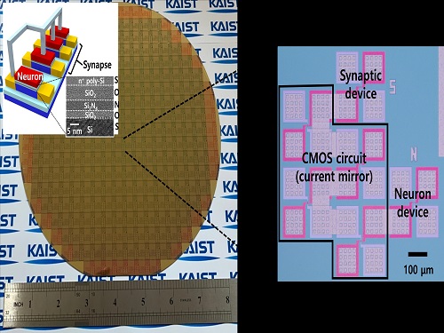 Brain-Inspired Highly Scalable Neuromorphic Hardware Presented
Neurons and synapses based on single transistor can dramatically reduce the hardware cost and accelerate the commercialization of neuromorphic hardware
KAIST researchers fabricated a brain-inspired highly scalable neuromorphic hardware by co-integrating single transistor neurons and synapses. Using standard silicon complementary metal-oxide-semiconductor (CMOS) technology, the neuromorphic hardware is expected to reduce chip cost and simplify fabrication procedures.
The research team led by Yang-Kyu Choi and Sung-Yool Choi produced a neurons and synapses based on single transistor for highly scalable neuromorphic hardware and showed the ability to recognize text and face images. This research was featured in Science Advances on August 4.
Neuromorphic hardware has attracted a great deal of attention because of its artificial intelligence functions, but consuming ultra-low power of less than 20 watts by mimicking the human brain. To make neuromorphic hardware work, a neuron that generates a spike when integrating a certain signal, and a synapse remembering the connection between two neurons are necessary, just like the biological brain. However, since neurons and synapses constructed on digital or analog circuits occupy a large space, there is a limit in terms of hardware efficiency and costs. Since the human brain consists of about 1011 neurons and 1014 synapses, it is necessary to improve the hardware cost in order to apply it to mobile and IoT devices.
To solve the problem, the research team mimicked the behavior of biological neurons and synapses with a single transistor, and co-integrated them onto an 8-inch wafer. The manufactured neuromorphic transistors have the same structure as the transistors for memory and logic that are currently mass-produced. In addition, the neuromorphic transistors proved for the first time that they can be implemented with a ‘Janus structure’ that functions as both neuron and synapse, just like coins have heads and tails.
Professor Yang-Kyu Choi said that this work can dramatically reduce the hardware cost by replacing the neurons and synapses that were based on complex digital and analog circuits with a single transistor. "We have demonstrated that neurons and synapses can be implemented using a single transistor," said Joon-Kyu Han, the first author. "By co-integrating single transistor neurons and synapses on the same wafer using a standard CMOS process, the hardware cost of the neuromorphic hardware has been improved, which will accelerate the commercialization of neuromorphic hardware,” Han added.This research was supported by the National Research Foundation (NRF) and IC Design Education Center (IDEC).
-PublicationJoon-Kyu Han, Sung-Yool Choi, Yang-Kyu Choi, et al.“Cointegration of single-transistor neurons and synapses by nanoscale CMOS fabrication for highly scalable neuromorphic hardware,” Science Advances (DOI: 10.1126/sciadv.abg8836)
-ProfileProfessor Yang-Kyu ChoiNano-Oriented Bio-Electronics Labhttps://sites.google.com/view/nobelab/
School of Electrical EngineeringKAIST
Professor Sung-Yool ChoiMolecular and Nano Device Laboratoryhttps://www.mndl.kaist.ac.kr/
School of Electrical EngineeringKAIST
2021.08.05 View 13354
Brain-Inspired Highly Scalable Neuromorphic Hardware Presented
Neurons and synapses based on single transistor can dramatically reduce the hardware cost and accelerate the commercialization of neuromorphic hardware
KAIST researchers fabricated a brain-inspired highly scalable neuromorphic hardware by co-integrating single transistor neurons and synapses. Using standard silicon complementary metal-oxide-semiconductor (CMOS) technology, the neuromorphic hardware is expected to reduce chip cost and simplify fabrication procedures.
The research team led by Yang-Kyu Choi and Sung-Yool Choi produced a neurons and synapses based on single transistor for highly scalable neuromorphic hardware and showed the ability to recognize text and face images. This research was featured in Science Advances on August 4.
Neuromorphic hardware has attracted a great deal of attention because of its artificial intelligence functions, but consuming ultra-low power of less than 20 watts by mimicking the human brain. To make neuromorphic hardware work, a neuron that generates a spike when integrating a certain signal, and a synapse remembering the connection between two neurons are necessary, just like the biological brain. However, since neurons and synapses constructed on digital or analog circuits occupy a large space, there is a limit in terms of hardware efficiency and costs. Since the human brain consists of about 1011 neurons and 1014 synapses, it is necessary to improve the hardware cost in order to apply it to mobile and IoT devices.
To solve the problem, the research team mimicked the behavior of biological neurons and synapses with a single transistor, and co-integrated them onto an 8-inch wafer. The manufactured neuromorphic transistors have the same structure as the transistors for memory and logic that are currently mass-produced. In addition, the neuromorphic transistors proved for the first time that they can be implemented with a ‘Janus structure’ that functions as both neuron and synapse, just like coins have heads and tails.
Professor Yang-Kyu Choi said that this work can dramatically reduce the hardware cost by replacing the neurons and synapses that were based on complex digital and analog circuits with a single transistor. "We have demonstrated that neurons and synapses can be implemented using a single transistor," said Joon-Kyu Han, the first author. "By co-integrating single transistor neurons and synapses on the same wafer using a standard CMOS process, the hardware cost of the neuromorphic hardware has been improved, which will accelerate the commercialization of neuromorphic hardware,” Han added.This research was supported by the National Research Foundation (NRF) and IC Design Education Center (IDEC).
-PublicationJoon-Kyu Han, Sung-Yool Choi, Yang-Kyu Choi, et al.“Cointegration of single-transistor neurons and synapses by nanoscale CMOS fabrication for highly scalable neuromorphic hardware,” Science Advances (DOI: 10.1126/sciadv.abg8836)
-ProfileProfessor Yang-Kyu ChoiNano-Oriented Bio-Electronics Labhttps://sites.google.com/view/nobelab/
School of Electrical EngineeringKAIST
Professor Sung-Yool ChoiMolecular and Nano Device Laboratoryhttps://www.mndl.kaist.ac.kr/
School of Electrical EngineeringKAIST
2021.08.05 View 13354 -
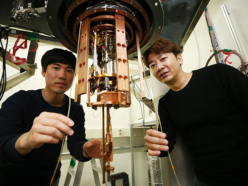
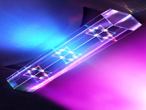 Quantum Laser Turns Energy Loss into Gain
A new laser that generates quantum particles can recycle lost energy for highly efficient, low threshold laser applications
Scientists at KAIST have fabricated a laser system that generates highly interactive quantum particles at room temperature. Their findings, published in the journal Nature Photonics, could lead to a single microcavity laser system that requires lower threshold energy as its energy loss increases.
The system, developed by KAIST physicist Yong-Hoon Cho and colleagues, involves shining light through a single hexagonal-shaped microcavity treated with a loss-modulated silicon nitride substrate. The system design leads to the generation of a polariton laser at room temperature, which is exciting because this usually requires cryogenic temperatures.
The researchers found another unique and counter-intuitive feature of this design. Normally, energy is lost during laser operation. But in this system, as energy loss increased, the amount of energy needed to induce lasing decreased. Exploiting this phenomenon could lead to the development of high efficiency, low threshold lasers for future quantum optical devices.
“This system applies a concept of quantum physics known as parity-time reversal symmetry,” explains Professor Cho. “This is an important platform that allows energy loss to be used as gain. It can be used to reduce laser threshold energy for classical optical devices and sensors, as well as quantum devices and controlling the direction of light.”
The key is the design and materials. The hexagonal microcavity divides light particles into two different modes: one that passes through the upward-facing triangle of the hexagon and another that passes through its downward-facing triangle. Both modes of light particles have the same energy and path but don’t interact with each other.
However, the light particles do interact with other particles called excitons, provided by the hexagonal microcavity, which is made of semiconductors. This interaction leads to the generation of new quantum particles called polaritons that then interact with each other to generate the polariton laser. By controlling the degree of loss between the microcavity and the semiconductor substrate, an intriguing phenomenon arises, with the threshold energy becoming smaller as energy loss increases. This research was supported by the Samsung Science and Technology Foundation and Korea’s National Research Foundation.
-PublicationSong,H.G, Choi, M, Woo, K.Y. Yong-Hoon Cho Room-temperature polaritonic non-Hermitian system with single microcavityNature Photonics (https://doi.org/10.1038/s41566-021-00820-z)
-ProfileProfessor Yong-Hoon ChoQuantum & Nanobio Photonics Laboratoryhttp://qnp.kaist.ac.kr/
Department of PhysicsKAIST
2021.07.07 View 12393
Quantum Laser Turns Energy Loss into Gain
A new laser that generates quantum particles can recycle lost energy for highly efficient, low threshold laser applications
Scientists at KAIST have fabricated a laser system that generates highly interactive quantum particles at room temperature. Their findings, published in the journal Nature Photonics, could lead to a single microcavity laser system that requires lower threshold energy as its energy loss increases.
The system, developed by KAIST physicist Yong-Hoon Cho and colleagues, involves shining light through a single hexagonal-shaped microcavity treated with a loss-modulated silicon nitride substrate. The system design leads to the generation of a polariton laser at room temperature, which is exciting because this usually requires cryogenic temperatures.
The researchers found another unique and counter-intuitive feature of this design. Normally, energy is lost during laser operation. But in this system, as energy loss increased, the amount of energy needed to induce lasing decreased. Exploiting this phenomenon could lead to the development of high efficiency, low threshold lasers for future quantum optical devices.
“This system applies a concept of quantum physics known as parity-time reversal symmetry,” explains Professor Cho. “This is an important platform that allows energy loss to be used as gain. It can be used to reduce laser threshold energy for classical optical devices and sensors, as well as quantum devices and controlling the direction of light.”
The key is the design and materials. The hexagonal microcavity divides light particles into two different modes: one that passes through the upward-facing triangle of the hexagon and another that passes through its downward-facing triangle. Both modes of light particles have the same energy and path but don’t interact with each other.
However, the light particles do interact with other particles called excitons, provided by the hexagonal microcavity, which is made of semiconductors. This interaction leads to the generation of new quantum particles called polaritons that then interact with each other to generate the polariton laser. By controlling the degree of loss between the microcavity and the semiconductor substrate, an intriguing phenomenon arises, with the threshold energy becoming smaller as energy loss increases. This research was supported by the Samsung Science and Technology Foundation and Korea’s National Research Foundation.
-PublicationSong,H.G, Choi, M, Woo, K.Y. Yong-Hoon Cho Room-temperature polaritonic non-Hermitian system with single microcavityNature Photonics (https://doi.org/10.1038/s41566-021-00820-z)
-ProfileProfessor Yong-Hoon ChoQuantum & Nanobio Photonics Laboratoryhttp://qnp.kaist.ac.kr/
Department of PhysicsKAIST
2021.07.07 View 12393 -
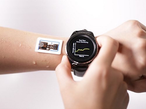 Wearable Device to Monitor Sweat in Real Time
An on-skin platform for the wireless monitoring of flow rate, cumulative loss, and temperature of sweat in real time
An electronic patch can monitor your sweating and check your health status. Even more, the soft microfluidic device that adheres to the surface of the skin, captures, stores, and performs biomarker analysis of sweat as it is released through the eccrine glands.
This wearable and wireless electronic device developed by Professor Kyeongha Kwon and her collaborators is a digital and wireless platform that could help track the so-called ‘filling process’ of sweat without having to visually examine the device. The platform was integrated with microfluidic systems to analyze the sweat’s components.
To monitor the sweat release rate in real time, the researchers created a ‘thermal flow sensing module.’ They designed a sophisticated microfluidic channel to allow the collected sweat to flow through a narrow passage and a heat source was placed on the outer surface of the channel to induce a heat exchange between the sweat and the heated channel.
As a result, the researchers could develop a wireless electronic patch that can measure the temperature difference in a specific location upstream and downstream of the heat source with an electronic circuit and convert it into a digital signal to measure the sweat release rate in real time. The patch accurately measured the perspiration rate in the range of 0-5 microliters/minute (μl/min), which was considered physiologically significant. The sensor can measure the flow of sweat directly and then use the information it collected to quantify total sweat loss. Moreover, the device features advanced microfluidic systems and colorimetric chemical reagents to gather pH measurements and determine the concentration of chloride, creatinine, and glucose in a user's sweat.
Professor Kwon said that these indicators could be used to diagnose various diseases related with sweating such as cystic fibrosis, diabetes, kidney dysfunction, and metabolic alkalosis. “As the sweat flowing in the microfluidic channel is completely separated from the electronic circuit, the new patch overcame the shortcomings of existing flow rate measuring devices, which were vulnerable to corrosion and aging,” she explained.
The patch can be easily attached to the skin with flexible circuit board printing technology and silicone sealing technology. It has an additional sensor that detects changes in skin temperature. Using a smartphone app, a user can check the data measured by the wearable patch in real time.
Professor Kwon added, “This patch can be widely used for personal hydration strategies, the detection of dehydration symptoms, and other health management purposes. It can also be used in a systematic drug delivery system, such as for measuring the blood flow rate in blood vessels near the skin’s surface or measuring a drug’s release rate in real time to calculate the exact dosage.”
-PublicationKyeongha Kwon, Jong Uk Kim, John A. Rogers, et al. “An on-skin platform for wireless monitoring of flow rate, cumulative loss and temperature of sweat in real time.” Nature Electronics (doi.org/10.1038/s41928-021-00556-2)
-ProfileProfessor Kyeongha KwonSchool of Electrical EngineeringKAIST
2021.06.25 View 13026
Wearable Device to Monitor Sweat in Real Time
An on-skin platform for the wireless monitoring of flow rate, cumulative loss, and temperature of sweat in real time
An electronic patch can monitor your sweating and check your health status. Even more, the soft microfluidic device that adheres to the surface of the skin, captures, stores, and performs biomarker analysis of sweat as it is released through the eccrine glands.
This wearable and wireless electronic device developed by Professor Kyeongha Kwon and her collaborators is a digital and wireless platform that could help track the so-called ‘filling process’ of sweat without having to visually examine the device. The platform was integrated with microfluidic systems to analyze the sweat’s components.
To monitor the sweat release rate in real time, the researchers created a ‘thermal flow sensing module.’ They designed a sophisticated microfluidic channel to allow the collected sweat to flow through a narrow passage and a heat source was placed on the outer surface of the channel to induce a heat exchange between the sweat and the heated channel.
As a result, the researchers could develop a wireless electronic patch that can measure the temperature difference in a specific location upstream and downstream of the heat source with an electronic circuit and convert it into a digital signal to measure the sweat release rate in real time. The patch accurately measured the perspiration rate in the range of 0-5 microliters/minute (μl/min), which was considered physiologically significant. The sensor can measure the flow of sweat directly and then use the information it collected to quantify total sweat loss. Moreover, the device features advanced microfluidic systems and colorimetric chemical reagents to gather pH measurements and determine the concentration of chloride, creatinine, and glucose in a user's sweat.
Professor Kwon said that these indicators could be used to diagnose various diseases related with sweating such as cystic fibrosis, diabetes, kidney dysfunction, and metabolic alkalosis. “As the sweat flowing in the microfluidic channel is completely separated from the electronic circuit, the new patch overcame the shortcomings of existing flow rate measuring devices, which were vulnerable to corrosion and aging,” she explained.
The patch can be easily attached to the skin with flexible circuit board printing technology and silicone sealing technology. It has an additional sensor that detects changes in skin temperature. Using a smartphone app, a user can check the data measured by the wearable patch in real time.
Professor Kwon added, “This patch can be widely used for personal hydration strategies, the detection of dehydration symptoms, and other health management purposes. It can also be used in a systematic drug delivery system, such as for measuring the blood flow rate in blood vessels near the skin’s surface or measuring a drug’s release rate in real time to calculate the exact dosage.”
-PublicationKyeongha Kwon, Jong Uk Kim, John A. Rogers, et al. “An on-skin platform for wireless monitoring of flow rate, cumulative loss and temperature of sweat in real time.” Nature Electronics (doi.org/10.1038/s41928-021-00556-2)
-ProfileProfessor Kyeongha KwonSchool of Electrical EngineeringKAIST
2021.06.25 View 13026 -
 Attachable Skin Monitors that Wick the Sweat Away
- A silicone membrane for wearable devices is more comfortable and breathable thanks to better-sized pores made with the help of citric acid crystals. -
A new preparation technique fabricates thin, silicone-based patches that rapidly wick water away from the skin. The technique could reduce the redness and itching caused by wearable biosensors that trap sweat beneath them. The technique was developed by bioengineer and professor Young-Ho Cho and his colleagues at KAIST and reported in the journal Scientific Reports last month.
“Wearable bioelectronics are becoming more attractive for the day-to-day monitoring of biological compounds found in sweat, like hormones or glucose, as well as body temperature, heart rate, and energy expenditure,” Professor Cho explained. “But currently available materials can cause skin irritation, so scientists are looking for ways to improve them,” he added.
Attachable biosensors often use a silicone-based compound called polydimethylsiloxane (PDMS), as it has a relatively high water vapour transmission rate compared to other materials. Still, this rate is only two-thirds that of skin’s water evaporation rate, meaning sweat still gets trapped underneath it.
Current fabrication approaches mix PDMS with beads or solutes, such as sugars or salts, and then remove them to leave pores in their place. Another technique uses gas to form pores in the material. Each technique has its disadvantages, from being expensive and complex to leaving pores of different sizes.
A team of researchers led by Professor Cho from the KAIST Department of Bio and Brain Engineering was able to form small, uniform pores by crystallizing citric acid in PDMS and then removing the crystals using ethanol. The approach is significantly cheaper than using beads, and leads to 93.2% smaller and 425% more uniformly-sized pores compared to using sugar. Importantly, the membrane transmits water vapour 2.2 times faster than human skin.
The team tested their membrane on human skin for seven days and found that it caused only minor redness and no itching, whereas a non-porous PDMS membrane did.
Professor Cho said, “Our method could be used to fabricate porous PDMS membranes for skin-attachable devices used for daily monitoring of physiological signals.”
“We next plan to modify our membrane so it can be more readily attached to and removed from skin,” he added.
This work was supported by the Ministry of Trade, Industry and Energy (MOTIE) of Korea under the Alchemist Project.
Image description:
Smaller, more uniformly-sized pores are made in the PDMS membrane by mixing PDMS, toluene, citric acid, and ethanol. Toluene dilutes PDMS so it can easily mix with the other two constituents. Toluene and ethanol are then evaporated, which causes the citric acid to crystallize within the PDMS material. The mixture is placed in a mould where it solidifies into a thin film. The crystals are then removed using ethanol, leaving pores in their place.
Image credit:
Professor Young-Ho Cho, KAIST
Image usage restrictions:
News organizations may use or redistribute this image, with proper attribution, as part of news coverage of this paper only.
Publication:
Yoon, S, et al. (2021) Wearable porous PDMS layer of high moisture permeability for skin trouble reduction. Scientific Reports 11, Article No. 938. Available online at https://doi.org/10.1038/s41598-020-78580-z
Profile:
Young-Ho Cho, Ph.D
Professor
mems@kaist.ac.kr
https://mems.kaist.ac.kr
NanoSentuating Systems Laboratory
Department of Bio and Brain Engineering
https://kaist.ac.kr
Korea Advanced Institute of Science and Technology (KAIST)
Daejeon, Republic of Korea
(END)
2021.02.22 View 15892
Attachable Skin Monitors that Wick the Sweat Away
- A silicone membrane for wearable devices is more comfortable and breathable thanks to better-sized pores made with the help of citric acid crystals. -
A new preparation technique fabricates thin, silicone-based patches that rapidly wick water away from the skin. The technique could reduce the redness and itching caused by wearable biosensors that trap sweat beneath them. The technique was developed by bioengineer and professor Young-Ho Cho and his colleagues at KAIST and reported in the journal Scientific Reports last month.
“Wearable bioelectronics are becoming more attractive for the day-to-day monitoring of biological compounds found in sweat, like hormones or glucose, as well as body temperature, heart rate, and energy expenditure,” Professor Cho explained. “But currently available materials can cause skin irritation, so scientists are looking for ways to improve them,” he added.
Attachable biosensors often use a silicone-based compound called polydimethylsiloxane (PDMS), as it has a relatively high water vapour transmission rate compared to other materials. Still, this rate is only two-thirds that of skin’s water evaporation rate, meaning sweat still gets trapped underneath it.
Current fabrication approaches mix PDMS with beads or solutes, such as sugars or salts, and then remove them to leave pores in their place. Another technique uses gas to form pores in the material. Each technique has its disadvantages, from being expensive and complex to leaving pores of different sizes.
A team of researchers led by Professor Cho from the KAIST Department of Bio and Brain Engineering was able to form small, uniform pores by crystallizing citric acid in PDMS and then removing the crystals using ethanol. The approach is significantly cheaper than using beads, and leads to 93.2% smaller and 425% more uniformly-sized pores compared to using sugar. Importantly, the membrane transmits water vapour 2.2 times faster than human skin.
The team tested their membrane on human skin for seven days and found that it caused only minor redness and no itching, whereas a non-porous PDMS membrane did.
Professor Cho said, “Our method could be used to fabricate porous PDMS membranes for skin-attachable devices used for daily monitoring of physiological signals.”
“We next plan to modify our membrane so it can be more readily attached to and removed from skin,” he added.
This work was supported by the Ministry of Trade, Industry and Energy (MOTIE) of Korea under the Alchemist Project.
Image description:
Smaller, more uniformly-sized pores are made in the PDMS membrane by mixing PDMS, toluene, citric acid, and ethanol. Toluene dilutes PDMS so it can easily mix with the other two constituents. Toluene and ethanol are then evaporated, which causes the citric acid to crystallize within the PDMS material. The mixture is placed in a mould where it solidifies into a thin film. The crystals are then removed using ethanol, leaving pores in their place.
Image credit:
Professor Young-Ho Cho, KAIST
Image usage restrictions:
News organizations may use or redistribute this image, with proper attribution, as part of news coverage of this paper only.
Publication:
Yoon, S, et al. (2021) Wearable porous PDMS layer of high moisture permeability for skin trouble reduction. Scientific Reports 11, Article No. 938. Available online at https://doi.org/10.1038/s41598-020-78580-z
Profile:
Young-Ho Cho, Ph.D
Professor
mems@kaist.ac.kr
https://mems.kaist.ac.kr
NanoSentuating Systems Laboratory
Department of Bio and Brain Engineering
https://kaist.ac.kr
Korea Advanced Institute of Science and Technology (KAIST)
Daejeon, Republic of Korea
(END)
2021.02.22 View 15892 -
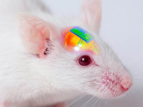 Wirelessly Rechargeable Soft Brain Implant Controls Brain Cells
Researchers have invented a smartphone-controlled soft brain implant that can be recharged wirelessly from outside the body. It enables long-term neural circuit manipulation without the need for periodic disruptive surgeries to replace the battery of the implant. Scientists believe this technology can help uncover and treat psychiatric disorders and neurodegenerative diseases such as addiction, depression, and Parkinson’s.
A group of KAIST researchers and collaborators have engineered a tiny brain implant that can be wirelessly recharged from outside the body to control brain circuits for long periods of time without battery replacement. The device is constructed of ultra-soft and bio-compliant polymers to help provide long-term compatibility with tissue. Geared with micrometer-sized LEDs (equivalent to the size of a grain of salt) mounted on ultrathin probes (the thickness of a human hair), it can wirelessly manipulate target neurons in the deep brain using light.
This study, led by Professor Jae-Woong Jeong, is a step forward from the wireless head-mounted implant neural device he developed in 2019. That previous version could indefinitely deliver multiple drugs and light stimulation treatment wirelessly by using a smartphone. For more, Manipulating Brain Cells by Smartphone.
For the new upgraded version, the research team came up with a fully implantable, soft optoelectronic system that can be remotely and selectively controlled by a smartphone. This research was published on January 22, 2021 in Nature Communications.
The new wireless charging technology addresses the limitations of current brain implants. Wireless implantable device technologies have recently become popular as alternatives to conventional tethered implants, because they help minimize stress and inflammation in freely-moving animals during brain studies, which in turn enhance the lifetime of the devices. However, such devices require either intermittent surgeries to replace discharged batteries, or special and bulky wireless power setups, which limit experimental options as well as the scalability of animal experiments.
“This powerful device eliminates the need for additional painful surgeries to replace an exhausted battery in the implant, allowing seamless chronic neuromodulation,” said Professor Jeong. “We believe that the same basic technology can be applied to various types of implants, including deep brain stimulators, and cardiac and gastric pacemakers, to reduce the burden on patients for long-term use within the body.”
To enable wireless battery charging and controls, researchers developed a tiny circuit that integrates a wireless energy harvester with a coil antenna and a Bluetooth low-energy chip. An alternating magnetic field can harmlessly penetrate through tissue, and generate electricity inside the device to charge the battery. Then the battery-powered Bluetooth implant delivers programmable patterns of light to brain cells using an “easy-to-use” smartphone app for real-time brain control.
“This device can be operated anywhere and anytime to manipulate neural circuits, which makes it a highly versatile tool for investigating brain functions,” said lead author Choong Yeon Kim, a researcher at KAIST.
Neuroscientists successfully tested these implants in rats and demonstrated their ability to suppress cocaine-induced behaviour after the rats were injected with cocaine. This was achieved by precise light stimulation of relevant target neurons in their brains using the smartphone-controlled LEDs. Furthermore, the battery in the implants could be repeatedly recharged while the rats were behaving freely, thus minimizing any physical interruption to the experiments.
“Wireless battery re-charging makes experimental procedures much less complicated,” said the co-lead author Min Jeong Ku, a researcher at Yonsei University’s College of Medicine.
“The fact that we can control a specific behaviour of animals, by delivering light stimulation into the brain just with a simple manipulation of smartphone app, watching freely moving animals nearby, is very interesting and stimulates a lot of imagination,” said Jeong-Hoon Kim, a professor of physiology at Yonsei University’s College of Medicine. “This technology will facilitate various avenues of brain research.”
The researchers believe this brain implant technology may lead to new opportunities for brain research and therapeutic intervention to treat diseases in the brain and other organs.
This work was supported by grants from the National Research Foundation of Korea and the KAIST Global Singularity Research Program.
-Profile
Professor Jae-Woong Jeong
https://www.jeongresearch.org/
School of Electrical Engineering
KAIST
2021.01.26 View 28443
Wirelessly Rechargeable Soft Brain Implant Controls Brain Cells
Researchers have invented a smartphone-controlled soft brain implant that can be recharged wirelessly from outside the body. It enables long-term neural circuit manipulation without the need for periodic disruptive surgeries to replace the battery of the implant. Scientists believe this technology can help uncover and treat psychiatric disorders and neurodegenerative diseases such as addiction, depression, and Parkinson’s.
A group of KAIST researchers and collaborators have engineered a tiny brain implant that can be wirelessly recharged from outside the body to control brain circuits for long periods of time without battery replacement. The device is constructed of ultra-soft and bio-compliant polymers to help provide long-term compatibility with tissue. Geared with micrometer-sized LEDs (equivalent to the size of a grain of salt) mounted on ultrathin probes (the thickness of a human hair), it can wirelessly manipulate target neurons in the deep brain using light.
This study, led by Professor Jae-Woong Jeong, is a step forward from the wireless head-mounted implant neural device he developed in 2019. That previous version could indefinitely deliver multiple drugs and light stimulation treatment wirelessly by using a smartphone. For more, Manipulating Brain Cells by Smartphone.
For the new upgraded version, the research team came up with a fully implantable, soft optoelectronic system that can be remotely and selectively controlled by a smartphone. This research was published on January 22, 2021 in Nature Communications.
The new wireless charging technology addresses the limitations of current brain implants. Wireless implantable device technologies have recently become popular as alternatives to conventional tethered implants, because they help minimize stress and inflammation in freely-moving animals during brain studies, which in turn enhance the lifetime of the devices. However, such devices require either intermittent surgeries to replace discharged batteries, or special and bulky wireless power setups, which limit experimental options as well as the scalability of animal experiments.
“This powerful device eliminates the need for additional painful surgeries to replace an exhausted battery in the implant, allowing seamless chronic neuromodulation,” said Professor Jeong. “We believe that the same basic technology can be applied to various types of implants, including deep brain stimulators, and cardiac and gastric pacemakers, to reduce the burden on patients for long-term use within the body.”
To enable wireless battery charging and controls, researchers developed a tiny circuit that integrates a wireless energy harvester with a coil antenna and a Bluetooth low-energy chip. An alternating magnetic field can harmlessly penetrate through tissue, and generate electricity inside the device to charge the battery. Then the battery-powered Bluetooth implant delivers programmable patterns of light to brain cells using an “easy-to-use” smartphone app for real-time brain control.
“This device can be operated anywhere and anytime to manipulate neural circuits, which makes it a highly versatile tool for investigating brain functions,” said lead author Choong Yeon Kim, a researcher at KAIST.
Neuroscientists successfully tested these implants in rats and demonstrated their ability to suppress cocaine-induced behaviour after the rats were injected with cocaine. This was achieved by precise light stimulation of relevant target neurons in their brains using the smartphone-controlled LEDs. Furthermore, the battery in the implants could be repeatedly recharged while the rats were behaving freely, thus minimizing any physical interruption to the experiments.
“Wireless battery re-charging makes experimental procedures much less complicated,” said the co-lead author Min Jeong Ku, a researcher at Yonsei University’s College of Medicine.
“The fact that we can control a specific behaviour of animals, by delivering light stimulation into the brain just with a simple manipulation of smartphone app, watching freely moving animals nearby, is very interesting and stimulates a lot of imagination,” said Jeong-Hoon Kim, a professor of physiology at Yonsei University’s College of Medicine. “This technology will facilitate various avenues of brain research.”
The researchers believe this brain implant technology may lead to new opportunities for brain research and therapeutic intervention to treat diseases in the brain and other organs.
This work was supported by grants from the National Research Foundation of Korea and the KAIST Global Singularity Research Program.
-Profile
Professor Jae-Woong Jeong
https://www.jeongresearch.org/
School of Electrical Engineering
KAIST
2021.01.26 View 28443 -
 Advanced NVMe Controller Technology for Next Generation Memory Devices
KAIST researchers advanced non-volatile memory express (NVMe) controller technology for next generation information storage devices, and made this new technology named ‘OpenExpress’ freely available to all universities and research institutes around the world to help reduce the research cost in related fields.
NVMe is a communication protocol made for high-performance storage devices based on a peripheral component interconnect-express (PCI-E) interface. NVMe has been developed to take the place of the Serial AT Attachment (SATA) protocol, which was developed to process data on hard disk drives (HDDs) and did not perform well in solid state drives (SSDs).
Unlike HDDs that use magnetic spinning disks, SSDs use semiconductor memory, allowing the rapid reading and writing of data. SSDs also generate less heat and noise, and are much more compact and lightweight.
Since data processing in SSDs using NVMe is up to six times faster than when SATA is used, NVMe has become the standard protocol for ultra-high speed and volume data processing, and is currently used in many flash-based information storage devices.
Studies on NVMe continue at both the academic and industrial levels, however, its poor accessibility is a drawback. Major information and communications technology (ICT) companies around the world expend astronomical costs to procure intellectual property (IP) related to hardware NVMe controllers, necessary for the use of NVMe. However, such IP is not publicly disclosed, making it difficult to be used by universities and research institutes for research purposes.
Although a small number of U.S. Silicon Valley startups provide parts of their independently developed IP for research, the cost of usage is around 34,000 USD per month. The costs skyrocket even further because each copy of single-use source code purchased for IP modification costs approximately 84,000 USD.
In order to address these issues, a group of researchers led by Professor Myoungsoo Jung from the School of Electrical Engineering at KAIST developed a next generation NVMe controller technology that achieved parallel data input/output processing for SSDs in a fully hardware automated form.
The researchers presented their work at the 2020 USENIX Annual Technical Conference (USENIX ATC ’20) in July, and released it as an open research framework named ‘OpenExpress.’
This NVMe controller technology developed by Professor Jung’s team comprises a wide range of basic hardware IP and key NVMe IP cores. To examine its actual performance, the team made an NVMe hardware controller prototype using OpenExpress, and designed all logics provided by OpenExpress to operate at high frequency.
The field-programmable gate array (FPGA) memory card prototype developed using OpenExpress demonstrated increased input/output data processing capacity per second, supporting up to 7 gigabit per second (GB/s) bandwidth. This makes it suitable for ultra-high speed and volume next generation memory device research.
In a test comparing various storage server loads on devices, the team’s FPGA also showed 76% higher bandwidth and 68% lower input/output delay compared to Intel’s new high performance SSD (Optane SSD), which is sufficient for many researchers studying systems employing future memory devices. Depending on user needs, silicon devices can be synthesized as well, which is expected to further enhance performance.
The NVMe controller technology of Professor Jung’s team can be freely used and modified under the OpenExpress open-source end-user agreement for non-commercial use by all universities and research institutes. This makes it extremely useful for research on next-generation memory compatible NVMe controllers and software stacks.
“With the product of this study being disclosed to the world, universities and research institutes can now use controllers that used to be exclusive for only the world’s biggest companies, at no cost,ˮ said Professor Jung. He went on to stress, “This is a meaningful first step in research of information storage device systems such as high-speed and volume next generation memory.”
This work was supported by a grant from MemRay, a company specializing in next generation memory development and distribution.
More details about the study can be found at http://camelab.org.
Image credit: Professor Myoungsoo Jung, KAIST
Image usage restrictions: News organizations may use or redistribute these figures and image, with proper attribution, as part of news coverage of this paper only.
-Publication:
Myoungsoo Jung. (2020). OpenExpress: Fully Hardware Automated Open Research Framework for Future Fast NVMe Devices. Presented in the Proceedings of the 2020 USENIX Annual Technical Conference (USENIX ATC ’20), Available online at https://www.usenix.org/system/files/atc20-jung.pdf
-Profile: Myoungsoo Jung
Associate Professor
m.jung@kaist.ac.kr
http://camelab.org
Computer Architecture and Memory Systems Laboratory
School of Electrical Engineering
http://kaist.ac.kr
Korea Advanced Institute of Science and Technology (KAIST)
Daejeon, Republic of Korea
(END)
2020.09.04 View 12925
Advanced NVMe Controller Technology for Next Generation Memory Devices
KAIST researchers advanced non-volatile memory express (NVMe) controller technology for next generation information storage devices, and made this new technology named ‘OpenExpress’ freely available to all universities and research institutes around the world to help reduce the research cost in related fields.
NVMe is a communication protocol made for high-performance storage devices based on a peripheral component interconnect-express (PCI-E) interface. NVMe has been developed to take the place of the Serial AT Attachment (SATA) protocol, which was developed to process data on hard disk drives (HDDs) and did not perform well in solid state drives (SSDs).
Unlike HDDs that use magnetic spinning disks, SSDs use semiconductor memory, allowing the rapid reading and writing of data. SSDs also generate less heat and noise, and are much more compact and lightweight.
Since data processing in SSDs using NVMe is up to six times faster than when SATA is used, NVMe has become the standard protocol for ultra-high speed and volume data processing, and is currently used in many flash-based information storage devices.
Studies on NVMe continue at both the academic and industrial levels, however, its poor accessibility is a drawback. Major information and communications technology (ICT) companies around the world expend astronomical costs to procure intellectual property (IP) related to hardware NVMe controllers, necessary for the use of NVMe. However, such IP is not publicly disclosed, making it difficult to be used by universities and research institutes for research purposes.
Although a small number of U.S. Silicon Valley startups provide parts of their independently developed IP for research, the cost of usage is around 34,000 USD per month. The costs skyrocket even further because each copy of single-use source code purchased for IP modification costs approximately 84,000 USD.
In order to address these issues, a group of researchers led by Professor Myoungsoo Jung from the School of Electrical Engineering at KAIST developed a next generation NVMe controller technology that achieved parallel data input/output processing for SSDs in a fully hardware automated form.
The researchers presented their work at the 2020 USENIX Annual Technical Conference (USENIX ATC ’20) in July, and released it as an open research framework named ‘OpenExpress.’
This NVMe controller technology developed by Professor Jung’s team comprises a wide range of basic hardware IP and key NVMe IP cores. To examine its actual performance, the team made an NVMe hardware controller prototype using OpenExpress, and designed all logics provided by OpenExpress to operate at high frequency.
The field-programmable gate array (FPGA) memory card prototype developed using OpenExpress demonstrated increased input/output data processing capacity per second, supporting up to 7 gigabit per second (GB/s) bandwidth. This makes it suitable for ultra-high speed and volume next generation memory device research.
In a test comparing various storage server loads on devices, the team’s FPGA also showed 76% higher bandwidth and 68% lower input/output delay compared to Intel’s new high performance SSD (Optane SSD), which is sufficient for many researchers studying systems employing future memory devices. Depending on user needs, silicon devices can be synthesized as well, which is expected to further enhance performance.
The NVMe controller technology of Professor Jung’s team can be freely used and modified under the OpenExpress open-source end-user agreement for non-commercial use by all universities and research institutes. This makes it extremely useful for research on next-generation memory compatible NVMe controllers and software stacks.
“With the product of this study being disclosed to the world, universities and research institutes can now use controllers that used to be exclusive for only the world’s biggest companies, at no cost,ˮ said Professor Jung. He went on to stress, “This is a meaningful first step in research of information storage device systems such as high-speed and volume next generation memory.”
This work was supported by a grant from MemRay, a company specializing in next generation memory development and distribution.
More details about the study can be found at http://camelab.org.
Image credit: Professor Myoungsoo Jung, KAIST
Image usage restrictions: News organizations may use or redistribute these figures and image, with proper attribution, as part of news coverage of this paper only.
-Publication:
Myoungsoo Jung. (2020). OpenExpress: Fully Hardware Automated Open Research Framework for Future Fast NVMe Devices. Presented in the Proceedings of the 2020 USENIX Annual Technical Conference (USENIX ATC ’20), Available online at https://www.usenix.org/system/files/atc20-jung.pdf
-Profile: Myoungsoo Jung
Associate Professor
m.jung@kaist.ac.kr
http://camelab.org
Computer Architecture and Memory Systems Laboratory
School of Electrical Engineering
http://kaist.ac.kr
Korea Advanced Institute of Science and Technology (KAIST)
Daejeon, Republic of Korea
(END)
2020.09.04 View 12925 -
 Black Phosphorous Tunnel Field-Effect Transistor as an Alternative Ultra-low Power Switch
Researchers have reported a black phosphorus transistor that can be used as an alternative ultra-low power switch. A research team led by Professor Sungjae Cho in the KAIST Department of Physics developed a thickness-controlled black phosphorous tunnel field-effect transistor (TFET) that shows 10-times lower switching power consumption as well as 10,000-times lower standby power consumption than conventional complementary metal-oxide-semiconductor (CMOS) transistors.
The research team said they developed fast and low-power transistors that can replace conventional CMOS transistors. In particular, they solved problems that have degraded TFET operation speed and performance, paving the way to extend Moore’s Law.
In the study featured in Nature Nanotechnology last month, Professor Cho’s team reported a natural heterojunction TFET with spatially varying layer thickness in black phosphorous without interface problems. They achieved record-low average subthreshold swing values over 4-5 dec of current and record-high, on-state current, which allows the TFETs to operate as fast as conventional CMOS transistors with as much lower power consumption.
"We successfully developed the first transistor that achieved the essential criteria for fast, low-power switching. Our newly developed TFETs can replace CMOS transistors by solving a major issue regarding the performance degradation of TFETs,"Professor Cho said.
The continuous down-scaling of transistors has been the key to the successful development of current information technology. However, with Moore’s Law reaching its limits due to the increased power consumption, the development of new alternative transistor designs has emerged as an urgent need.
Reducing both switching and standby power consumption while further scaling transistors requires overcoming the thermionic limit of subthreshold swing, which is defined as the required voltage per ten-fold current increase in the subthreshold region. In order to reduce both the switching and standby power of CMOS circuits, it is critical to reduce the subthreshold swing of the transistors.
However, there is fundamental subthreshold swing limit of 60 mV/dec in CMOS transistors, which originates from thermal carrier injection. The International Roadmap for Devices and Systems has already predicted that new device geometries with new materials beyond CMOS will be required to address transistor scaling challenges in the near future. In particular, TFETs have been suggested as a major alternative to CMOS transistors, since the subthreshold swing in TFETs can be substantially reduced below the thermionic limit of 60 mV/dec. TFETs operate via quantum tunneling, which does not limit subthreshold swing as in thermal injection of CMOS transistors.
In particular, heterojunction TFETs hold significant promise for delivering both low subthreshold swing and high on-state current. High on-current is essential for the fast operation of transistors since charging a device to on state takes a longer time with lower currents. Unlike theoretical expectations, previously developed heterojunction TFETs show 100-100,000x lower on-state current (100-100,000x slower operation speeds) than CMOS transistors due to interface problems in the heterojunction. This low operation speed impedes the replacement of CMOS transistors with low-power TFETs.
Professor Cho said, “We have demonstrated for the first time, to the best of our knowledge, TFET optimization for both fast and ultra-low-power operations, which is essential to replace CMOS transistors for low-power applications.” He said he is very delighted to extend Moore’s Law, which may eventually affect almost every aspect of life and society. This study (https://doi.org/10.1038/s41565-019-0623-7) was supported by the National Research Foundation of Korea.
Publication:
Kim et al. (2020) Thickness-controlled black phosphorus tunnel field-effect transistor for low-power switches. Nature Nanotechnology. Available online at https://doi.org/10.1038/s41565-019-0623-7
Profile:
Professor Sungjae Cho
sungjae.cho@kaist.ac.kr
Department of Physics
http://qtak.kaist.ac.kr/
KAIST
Profile:
Seungho Kim, PhD Candidate
krksh21@kaist.ac.kr
Department of Physics
http://qtak.kaist.ac.kr/
KAIST
(END)
2020.02.21 View 14247
Black Phosphorous Tunnel Field-Effect Transistor as an Alternative Ultra-low Power Switch
Researchers have reported a black phosphorus transistor that can be used as an alternative ultra-low power switch. A research team led by Professor Sungjae Cho in the KAIST Department of Physics developed a thickness-controlled black phosphorous tunnel field-effect transistor (TFET) that shows 10-times lower switching power consumption as well as 10,000-times lower standby power consumption than conventional complementary metal-oxide-semiconductor (CMOS) transistors.
The research team said they developed fast and low-power transistors that can replace conventional CMOS transistors. In particular, they solved problems that have degraded TFET operation speed and performance, paving the way to extend Moore’s Law.
In the study featured in Nature Nanotechnology last month, Professor Cho’s team reported a natural heterojunction TFET with spatially varying layer thickness in black phosphorous without interface problems. They achieved record-low average subthreshold swing values over 4-5 dec of current and record-high, on-state current, which allows the TFETs to operate as fast as conventional CMOS transistors with as much lower power consumption.
"We successfully developed the first transistor that achieved the essential criteria for fast, low-power switching. Our newly developed TFETs can replace CMOS transistors by solving a major issue regarding the performance degradation of TFETs,"Professor Cho said.
The continuous down-scaling of transistors has been the key to the successful development of current information technology. However, with Moore’s Law reaching its limits due to the increased power consumption, the development of new alternative transistor designs has emerged as an urgent need.
Reducing both switching and standby power consumption while further scaling transistors requires overcoming the thermionic limit of subthreshold swing, which is defined as the required voltage per ten-fold current increase in the subthreshold region. In order to reduce both the switching and standby power of CMOS circuits, it is critical to reduce the subthreshold swing of the transistors.
However, there is fundamental subthreshold swing limit of 60 mV/dec in CMOS transistors, which originates from thermal carrier injection. The International Roadmap for Devices and Systems has already predicted that new device geometries with new materials beyond CMOS will be required to address transistor scaling challenges in the near future. In particular, TFETs have been suggested as a major alternative to CMOS transistors, since the subthreshold swing in TFETs can be substantially reduced below the thermionic limit of 60 mV/dec. TFETs operate via quantum tunneling, which does not limit subthreshold swing as in thermal injection of CMOS transistors.
In particular, heterojunction TFETs hold significant promise for delivering both low subthreshold swing and high on-state current. High on-current is essential for the fast operation of transistors since charging a device to on state takes a longer time with lower currents. Unlike theoretical expectations, previously developed heterojunction TFETs show 100-100,000x lower on-state current (100-100,000x slower operation speeds) than CMOS transistors due to interface problems in the heterojunction. This low operation speed impedes the replacement of CMOS transistors with low-power TFETs.
Professor Cho said, “We have demonstrated for the first time, to the best of our knowledge, TFET optimization for both fast and ultra-low-power operations, which is essential to replace CMOS transistors for low-power applications.” He said he is very delighted to extend Moore’s Law, which may eventually affect almost every aspect of life and society. This study (https://doi.org/10.1038/s41565-019-0623-7) was supported by the National Research Foundation of Korea.
Publication:
Kim et al. (2020) Thickness-controlled black phosphorus tunnel field-effect transistor for low-power switches. Nature Nanotechnology. Available online at https://doi.org/10.1038/s41565-019-0623-7
Profile:
Professor Sungjae Cho
sungjae.cho@kaist.ac.kr
Department of Physics
http://qtak.kaist.ac.kr/
KAIST
Profile:
Seungho Kim, PhD Candidate
krksh21@kaist.ac.kr
Department of Physics
http://qtak.kaist.ac.kr/
KAIST
(END)
2020.02.21 View 14247 -
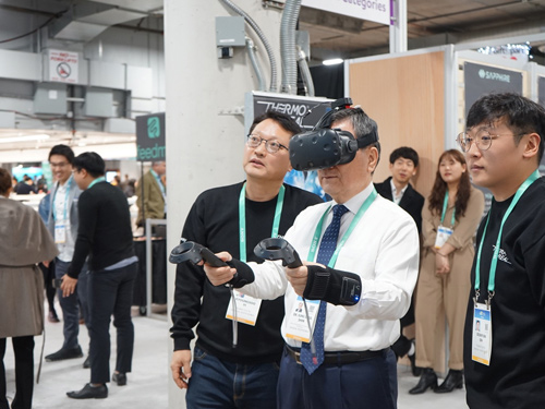 KAIST Showcases Advanced Technologies at CES 2020
< President Sung-Chul Shin experiencing cooling gaming headset developed by TEGWAY >
KAIST Pavilion showcased 12 KAIST startups and alumni companies’ technologies at the International Consumer Electronics Show (CES) 2020 held in Las Vegas last month. Especially four companies, TEGWAY, THE.WAVE.TALK, Sherpa Space, and LiBEST won the CES 2020 Innovation Awards presented by the Consumer Technology Association (CTA). The CTA selects the most innovative items from among all submissions.
TEGWAY spinned off by KAIST Professor Byung Jin Cho already made international headlines for their flexible, wearable, and temperature immersive thermoelectric device. The device was selected as one of the top ten most promising digital technologies by the Netexplo Forum in 2015, and has been expanded into VR, AR, and games.
THE.WAVE.TALK has developed their first home appliance product in collaboration with ID+IM Design Laboratory of KAIST in which Professor Sang-Min Bae heads as creative director. Their real-time bacteria analysis with smart IoT sensor won the home appliances section.
Sherpa Space and LiBEST are the alumni companies. Sherpa Space’s lighting for plants won the sustainability, eco-design, and smart energy section, and LiBEST’s full-range flexible battery won the section for technology for a better world.
KAIST’s Alumni Association, Development Foundation, and the Office of University-Industry Cooperation (OUIC) made every effort to present KAIST technologies to the global market. President Sung-Chul Shin led the delegation comprising of 70 faculty, researchers, and young entrepreneurs. The KAIST Alumni Association fully funded the traveling costs of 30 alumni entrepreneurs and students, establishing scholarship for the CES participation. Ten young entrepreneurs were selected through the KAIST Startup Awards, and 20 current students preparing to start their own companies were selected via recommendation from the respective departments.
Associate Vice President of the OUIC Kyung Cheol Choi said in excitement, “We received many offers for joint research and investment from leading companies around the world,” adding, “We will continue doing our best to generate global value by developing the innovative technologies obtained from education and research into businesses.”
The KAIST pavilion at CES 2020 showcased:
1. flexible thermoelectric device ThermoReal and cooling gaming headset from TEGWAY,
2. wearable flexible battery from LiBEST,
3. applications such as conductive transparent electrode film and transparent heating film from J-Micro,
4. on-device AI solution based on deep learning model compression technology from Nota,
5. portable high resolution brain imaging device from OBELAB,
6. real-time bacteria analysis technology from THE.WAVE.TALK,
7. conversation-based AI-1 radio service platform from Timecode Archive,
8. light source solutions for different stages in a plant’s life cycle from Sherpa Space,
9. skin attached micro-LED patch and flexible piezoelectric acoustic sensor from FRONICS,
10. real-time cardiovascular measurement device from Healthrian,
11. block chain based mobile research documentation system from ReDWit, and
12. student-developed comprehensive healthcare device using a smart mirror.
(END)
2020.01.13 View 14377
KAIST Showcases Advanced Technologies at CES 2020
< President Sung-Chul Shin experiencing cooling gaming headset developed by TEGWAY >
KAIST Pavilion showcased 12 KAIST startups and alumni companies’ technologies at the International Consumer Electronics Show (CES) 2020 held in Las Vegas last month. Especially four companies, TEGWAY, THE.WAVE.TALK, Sherpa Space, and LiBEST won the CES 2020 Innovation Awards presented by the Consumer Technology Association (CTA). The CTA selects the most innovative items from among all submissions.
TEGWAY spinned off by KAIST Professor Byung Jin Cho already made international headlines for their flexible, wearable, and temperature immersive thermoelectric device. The device was selected as one of the top ten most promising digital technologies by the Netexplo Forum in 2015, and has been expanded into VR, AR, and games.
THE.WAVE.TALK has developed their first home appliance product in collaboration with ID+IM Design Laboratory of KAIST in which Professor Sang-Min Bae heads as creative director. Their real-time bacteria analysis with smart IoT sensor won the home appliances section.
Sherpa Space and LiBEST are the alumni companies. Sherpa Space’s lighting for plants won the sustainability, eco-design, and smart energy section, and LiBEST’s full-range flexible battery won the section for technology for a better world.
KAIST’s Alumni Association, Development Foundation, and the Office of University-Industry Cooperation (OUIC) made every effort to present KAIST technologies to the global market. President Sung-Chul Shin led the delegation comprising of 70 faculty, researchers, and young entrepreneurs. The KAIST Alumni Association fully funded the traveling costs of 30 alumni entrepreneurs and students, establishing scholarship for the CES participation. Ten young entrepreneurs were selected through the KAIST Startup Awards, and 20 current students preparing to start their own companies were selected via recommendation from the respective departments.
Associate Vice President of the OUIC Kyung Cheol Choi said in excitement, “We received many offers for joint research and investment from leading companies around the world,” adding, “We will continue doing our best to generate global value by developing the innovative technologies obtained from education and research into businesses.”
The KAIST pavilion at CES 2020 showcased:
1. flexible thermoelectric device ThermoReal and cooling gaming headset from TEGWAY,
2. wearable flexible battery from LiBEST,
3. applications such as conductive transparent electrode film and transparent heating film from J-Micro,
4. on-device AI solution based on deep learning model compression technology from Nota,
5. portable high resolution brain imaging device from OBELAB,
6. real-time bacteria analysis technology from THE.WAVE.TALK,
7. conversation-based AI-1 radio service platform from Timecode Archive,
8. light source solutions for different stages in a plant’s life cycle from Sherpa Space,
9. skin attached micro-LED patch and flexible piezoelectric acoustic sensor from FRONICS,
10. real-time cardiovascular measurement device from Healthrian,
11. block chain based mobile research documentation system from ReDWit, and
12. student-developed comprehensive healthcare device using a smart mirror.
(END)
2020.01.13 View 14377 -
 ‘Carrier-Resolved Photo-Hall’ to Push Semiconductor Advances
(Professor Shin and Dr. Gunawan (left))
An IBM-KAIST research team described a breakthrough in a 140-year-old mystery in physics. The research reported in Nature last month unlocks the physical characteristics of semiconductors in much greater detail and aids in the development of new and improved semiconductor materials.
Research team under Professor Byungha Shin at the Department of Material Sciences and Engineering and Dr. Oki Gunawan at IBM discovered a new formula and technique that enables the simultaneous extraction of both majority and minority carrier information such as their density and mobility, as well as gain additional insights about carrier lifetimes, diffusion lengths, and the recombination process. This new discovery and technology will help push semiconductor advances in both existing and emerging technologies.
Semiconductors are the basic building blocks of today’s digital electronics age, providing us with a multitude of devices that benefit our modern life. To truly appreciate the physics of semiconductors, it is very important to understand the fundamental properties of the charge carriers inside the materials, whether those particles are positive or negative, their speed under an applied electric field, and how densely they are packed into the material.
Physicist Edwin Hall found a way to determine those properties in 1879, when he discovered that a magnetic field will deflect the movement of electronic charges inside a conductor and that the amount of deflection can be measured as a voltage perpendicular to the flow of the charge. Decades after Hall’s discovery, researchers also recognized that they can measure the Hall effect with light via “photo-Hall experiments”. During such experiments, the light generates multiple carriers or electron–hole pairs in the semiconductors.
Unfortunately, the basic Hall effect only provided insights into the dominant charge carrier (or majority carrier). Researchers were unable to extract the properties of both carriers (the majority and minority carriers) simultaneously. The property information of both carriers is crucial for many applications that involve light such as solar cells and other optoelectronic devices.
In the photo-Hall experiment by the KAIST-IBM team, both carriers contribute to changes in conductivity and the Hall coefficient. The key insight comes from measuring the conductivity and Hall coefficient as a function of light intensity. Hidden in the trajectory of the conductivity, the Hall coefficient curve reveals crucial new information: the difference in the mobility of both carriers. As discussed in the paper, this relationship can be expressed elegantly as: Δµ = d (σ²H)/dσ
The research team solved for both majority and minority carrier mobility and density as a function of light intensity, naming the new technique Carrier-Resolved Photo Hall (CRPH) measurement. With known light illumination intensity, the carrier lifetime can be established in a similar way.
Beyond advances in theoretical understanding, advances in experimental techniques were also critical for enabling this breakthrough. The technique requires a clean Hall signal measurement, which can be challenging for materials where the Hall signal is weak due to low mobility or when extra unwanted signals are present, such as under strong light illumination.
The newly developed photo-Hall technique allows the extraction of an astonishing amount of information from semiconductors. In contrast to only three parameters obtained in the classic Hall measurements, this new technique yields up to seven parameters at every tested level of light intensity. These include the mobility of both the electron and hole; their carrier density under light; the recombination lifetime; and the diffusion lengths for electrons, holes, and ambipolar types. All of these can be repeated N times (i.e. the number of light intensity settings used in the experiment).
Professor Shin said, “This novel technology sheds new light on understanding the physical characteristics of semiconductor materials in great detail.” Dr. Gunawan added, “This will will help accelerate the development of next-generation semiconductor technology such as better solar cells, better optoelectronics devices, and new materials and devices for artificial intelligence technology.”
Profile:
Professor Byungha Shin
Department of Materials Science and Engineering
KAIST
byungha@kaist.ac.kr
http://energymatlab.kaist.ac.kr/
2019.11.18 View 16408
‘Carrier-Resolved Photo-Hall’ to Push Semiconductor Advances
(Professor Shin and Dr. Gunawan (left))
An IBM-KAIST research team described a breakthrough in a 140-year-old mystery in physics. The research reported in Nature last month unlocks the physical characteristics of semiconductors in much greater detail and aids in the development of new and improved semiconductor materials.
Research team under Professor Byungha Shin at the Department of Material Sciences and Engineering and Dr. Oki Gunawan at IBM discovered a new formula and technique that enables the simultaneous extraction of both majority and minority carrier information such as their density and mobility, as well as gain additional insights about carrier lifetimes, diffusion lengths, and the recombination process. This new discovery and technology will help push semiconductor advances in both existing and emerging technologies.
Semiconductors are the basic building blocks of today’s digital electronics age, providing us with a multitude of devices that benefit our modern life. To truly appreciate the physics of semiconductors, it is very important to understand the fundamental properties of the charge carriers inside the materials, whether those particles are positive or negative, their speed under an applied electric field, and how densely they are packed into the material.
Physicist Edwin Hall found a way to determine those properties in 1879, when he discovered that a magnetic field will deflect the movement of electronic charges inside a conductor and that the amount of deflection can be measured as a voltage perpendicular to the flow of the charge. Decades after Hall’s discovery, researchers also recognized that they can measure the Hall effect with light via “photo-Hall experiments”. During such experiments, the light generates multiple carriers or electron–hole pairs in the semiconductors.
Unfortunately, the basic Hall effect only provided insights into the dominant charge carrier (or majority carrier). Researchers were unable to extract the properties of both carriers (the majority and minority carriers) simultaneously. The property information of both carriers is crucial for many applications that involve light such as solar cells and other optoelectronic devices.
In the photo-Hall experiment by the KAIST-IBM team, both carriers contribute to changes in conductivity and the Hall coefficient. The key insight comes from measuring the conductivity and Hall coefficient as a function of light intensity. Hidden in the trajectory of the conductivity, the Hall coefficient curve reveals crucial new information: the difference in the mobility of both carriers. As discussed in the paper, this relationship can be expressed elegantly as: Δµ = d (σ²H)/dσ
The research team solved for both majority and minority carrier mobility and density as a function of light intensity, naming the new technique Carrier-Resolved Photo Hall (CRPH) measurement. With known light illumination intensity, the carrier lifetime can be established in a similar way.
Beyond advances in theoretical understanding, advances in experimental techniques were also critical for enabling this breakthrough. The technique requires a clean Hall signal measurement, which can be challenging for materials where the Hall signal is weak due to low mobility or when extra unwanted signals are present, such as under strong light illumination.
The newly developed photo-Hall technique allows the extraction of an astonishing amount of information from semiconductors. In contrast to only three parameters obtained in the classic Hall measurements, this new technique yields up to seven parameters at every tested level of light intensity. These include the mobility of both the electron and hole; their carrier density under light; the recombination lifetime; and the diffusion lengths for electrons, holes, and ambipolar types. All of these can be repeated N times (i.e. the number of light intensity settings used in the experiment).
Professor Shin said, “This novel technology sheds new light on understanding the physical characteristics of semiconductor materials in great detail.” Dr. Gunawan added, “This will will help accelerate the development of next-generation semiconductor technology such as better solar cells, better optoelectronics devices, and new materials and devices for artificial intelligence technology.”
Profile:
Professor Byungha Shin
Department of Materials Science and Engineering
KAIST
byungha@kaist.ac.kr
http://energymatlab.kaist.ac.kr/
2019.11.18 View 16408 -
 Two More Cross-generation Collaborative Labs Open
< President Sung-Chul Shin (sixth from the left) and Professor Sun Chang Kim (seventh from the left) at the signboard ceremony of KAIST BioDesigneering Laboratory >
KAIST opened two more cross-generation collaborative labs last month. KAIST BioDesigneering Laboratory headed by Professor Sun Chang Kim from the Department of Biological Sciences and Nanophotonics Laboratory led by Professor Yong-Hee Lee from the Department of Physics have been selected to receive 500 million KRW funding for five years.
A four-member selection committee including the former President of ETH Zürich Professor Emeritus Ralph Eichler and Professor Kwang-Soo Kim of Harvard Medical School conducted a three-month review and evaluation for this selection to be made. With these two new labs onboard, a total of six cross-generation collaborative labs will be operated on campus.
The operation of cross-generation collaborative labs has been in trial since March last year, as one of the KAIST’s Vision 2031 research innovation initiatives. This novel approach is to pair up senior and junior faculty members for sustaining research and academic achievements even after the senior researcher retires, so that the spectrum of knowledge and research competitiveness can be extended to future generations. The selected labs will be funded for five years, and the funding will be extended if necessary. KAIST will continue to select new labs every year.
One of this year’s selectees Professor Sun Chang Kim will be teamed up with Professor Byung-Kwan Cho from the same department and Professor Jung Kyoon Choi from the Department of Bio and Brain Engineering to collaborate in the fields of synthetic biology, systems biology, and genetic engineering. This group mainly aims at designing and synthesizing optimal genomes that can efficiently manufacture protein drug and biomedical active materials. They will also strive to secure large amounts of high-functioning natural active substances, new adhesive antibacterial peptides, and eco-friendly ecological restoration materials. It is expected that collaboration between these three multigenerational professors will help innovate their bio-convergence technology and further strengthen their international competitiveness in the global bio-market.
Another world-renowned scholar Professor Yong-Hee Lee of photonic crystal laser study will be joined by Professor Minkyo Seo from the same department and Professor Hansuek Lee from the Graduate School of Nanoscience and Technology. They will explore the extreme limits of light-material interaction based on optical micro/nano resonators, with the goal of developing future nonlinear optoelectronic and quantum optical devices. The knowledge and technology newly gained from the research are expected to provide an important platform for a diverse range of fields from quantum communications to biophysics.
(END)
2019.09.06 View 12808
Two More Cross-generation Collaborative Labs Open
< President Sung-Chul Shin (sixth from the left) and Professor Sun Chang Kim (seventh from the left) at the signboard ceremony of KAIST BioDesigneering Laboratory >
KAIST opened two more cross-generation collaborative labs last month. KAIST BioDesigneering Laboratory headed by Professor Sun Chang Kim from the Department of Biological Sciences and Nanophotonics Laboratory led by Professor Yong-Hee Lee from the Department of Physics have been selected to receive 500 million KRW funding for five years.
A four-member selection committee including the former President of ETH Zürich Professor Emeritus Ralph Eichler and Professor Kwang-Soo Kim of Harvard Medical School conducted a three-month review and evaluation for this selection to be made. With these two new labs onboard, a total of six cross-generation collaborative labs will be operated on campus.
The operation of cross-generation collaborative labs has been in trial since March last year, as one of the KAIST’s Vision 2031 research innovation initiatives. This novel approach is to pair up senior and junior faculty members for sustaining research and academic achievements even after the senior researcher retires, so that the spectrum of knowledge and research competitiveness can be extended to future generations. The selected labs will be funded for five years, and the funding will be extended if necessary. KAIST will continue to select new labs every year.
One of this year’s selectees Professor Sun Chang Kim will be teamed up with Professor Byung-Kwan Cho from the same department and Professor Jung Kyoon Choi from the Department of Bio and Brain Engineering to collaborate in the fields of synthetic biology, systems biology, and genetic engineering. This group mainly aims at designing and synthesizing optimal genomes that can efficiently manufacture protein drug and biomedical active materials. They will also strive to secure large amounts of high-functioning natural active substances, new adhesive antibacterial peptides, and eco-friendly ecological restoration materials. It is expected that collaboration between these three multigenerational professors will help innovate their bio-convergence technology and further strengthen their international competitiveness in the global bio-market.
Another world-renowned scholar Professor Yong-Hee Lee of photonic crystal laser study will be joined by Professor Minkyo Seo from the same department and Professor Hansuek Lee from the Graduate School of Nanoscience and Technology. They will explore the extreme limits of light-material interaction based on optical micro/nano resonators, with the goal of developing future nonlinear optoelectronic and quantum optical devices. The knowledge and technology newly gained from the research are expected to provide an important platform for a diverse range of fields from quantum communications to biophysics.
(END)
2019.09.06 View 12808 -
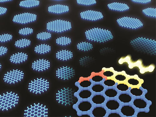 Synthesizing Single-Crystalline Hexagonal Graphene Quantum Dots
(Figure: Uniformly ordered single-crystalline graphene quantum dots of various sizes synthesized through solution chemistry.)
A KAIST team has designed a novel strategy for synthesizing single-crystalline graphene quantum dots, which emit stable blue light. The research team confirmed that a display made of their synthesized graphene quantum dots successfully emitted blue light with stable electric pressure, reportedly resolving the long-standing challenges of blue light emission in manufactured displays. The study, led by Professor O Ok Park in the Department of Chemical and Biological Engineering, was featured online in Nano Letters on July 5.
Graphene has gained increased attention as a next-generation material for its heat and electrical conductivity as well as its transparency. However, single and multi-layered graphene have characteristics of a conductor so that it is difficult to apply into semiconductor. Only when downsized to the nanoscale, semiconductor’s distinct feature of bandgap will be exhibited to emit the light in the graphene. This illuminating featuring of dot is referred to as a graphene quantum dot.
Conventionally, single-crystalline graphene has been fabricated by chemical vapor deposition (CVD) on copper or nickel thin films, or by peeling graphite physically and chemically. However, graphene made via chemical vapor deposition is mainly used for large-surface transparent electrodes. Meanwhile, graphene made by chemical and physical peeling carries uneven size defects.
The research team explained that their graphene quantum dots exhibited a very stable single-phase reaction when they mixed amine and acetic acid with an aqueous solution of glucose. Then, they synthesized single-crystalline graphene quantum dots from the self-assembly of the reaction intermediate. In the course of fabrication, the team developed a new separation method at a low-temperature precipitation, which led to successfully creating a homogeneous nucleation of graphene quantum dots via a single-phase reaction.
Professor Park and his colleagues have developed solution phase synthesis technology that allows for the creation of the desired crystal size for single nanocrystals down to 100 nano meters. It is reportedly the first synthesis of the homogeneous nucleation of graphene through a single-phase reaction.
Professor Park said, "This solution method will significantly contribute to the grafting of graphene in various fields. The application of this new graphene will expand the scope of its applications such as for flexible displays and varistors.”
This research was a joint project with a team from Korea University under Professor Sang Hyuk Im from the Department of Chemical and Biological Engineering, and was supported by the National Research Foundation of Korea, the Nano-Material Technology Development Program from the Electronics and Telecommunications Research Institute (ETRI), KAIST EEWS, and the BK21+ project from the Korean government.
2019.08.02 View 36482
Synthesizing Single-Crystalline Hexagonal Graphene Quantum Dots
(Figure: Uniformly ordered single-crystalline graphene quantum dots of various sizes synthesized through solution chemistry.)
A KAIST team has designed a novel strategy for synthesizing single-crystalline graphene quantum dots, which emit stable blue light. The research team confirmed that a display made of their synthesized graphene quantum dots successfully emitted blue light with stable electric pressure, reportedly resolving the long-standing challenges of blue light emission in manufactured displays. The study, led by Professor O Ok Park in the Department of Chemical and Biological Engineering, was featured online in Nano Letters on July 5.
Graphene has gained increased attention as a next-generation material for its heat and electrical conductivity as well as its transparency. However, single and multi-layered graphene have characteristics of a conductor so that it is difficult to apply into semiconductor. Only when downsized to the nanoscale, semiconductor’s distinct feature of bandgap will be exhibited to emit the light in the graphene. This illuminating featuring of dot is referred to as a graphene quantum dot.
Conventionally, single-crystalline graphene has been fabricated by chemical vapor deposition (CVD) on copper or nickel thin films, or by peeling graphite physically and chemically. However, graphene made via chemical vapor deposition is mainly used for large-surface transparent electrodes. Meanwhile, graphene made by chemical and physical peeling carries uneven size defects.
The research team explained that their graphene quantum dots exhibited a very stable single-phase reaction when they mixed amine and acetic acid with an aqueous solution of glucose. Then, they synthesized single-crystalline graphene quantum dots from the self-assembly of the reaction intermediate. In the course of fabrication, the team developed a new separation method at a low-temperature precipitation, which led to successfully creating a homogeneous nucleation of graphene quantum dots via a single-phase reaction.
Professor Park and his colleagues have developed solution phase synthesis technology that allows for the creation of the desired crystal size for single nanocrystals down to 100 nano meters. It is reportedly the first synthesis of the homogeneous nucleation of graphene through a single-phase reaction.
Professor Park said, "This solution method will significantly contribute to the grafting of graphene in various fields. The application of this new graphene will expand the scope of its applications such as for flexible displays and varistors.”
This research was a joint project with a team from Korea University under Professor Sang Hyuk Im from the Department of Chemical and Biological Engineering, and was supported by the National Research Foundation of Korea, the Nano-Material Technology Development Program from the Electronics and Telecommunications Research Institute (ETRI), KAIST EEWS, and the BK21+ project from the Korean government.
2019.08.02 View 36482