School+of+Electrical+Engineering
-
 The World’s First Hacking-preventing Cryptographic Semiconductor Chip
With the dramatic increase in the amount of information exchanged between components or devices in the 5G/6G era, such as for the Internet of Things (IoT) and autonomous driving, hacking attacks are becoming more sophisticated. Consequently, enhancing security functions is essential for safely transmitting data between and among devices.
On February 29th, a KAIST research team led by Professors Yang-gyu Choi and Seung-tak Ryu from the School of Electrical Engineering announced the successful development of the world's first security cryptographic semiconductor.
The team has developed the Cryptoristor, a cryptographic transistor based on FinFET technology, produced through a 100% silicon-compatible process, for the first time in the world. Cryptoristor is a random number generator (RNG) with unparalleled characteristics, featuring a unique structure comprising a single transistor and a distinctive mechanism.
In all security environments, including artificial intelligence, the most crucial element is the RNG. In the most commonly used security chip, the Advanced Encryption Standard (AES), the RNG is a core component, occupying approximately 75% of the total chip area and more than 85% of its energy consumption. Hence, there is an urgent need for the development of low-power/ultra-small RNGs suitable for mobile or IoT devices.
Existing RNGs come with limitations as they lack compatibility with silicon CMOS processes and circuit-based RNGs occupy a large surface area.
In contrast, the team’s newly developed Cryptoristor, a cryptographic semiconductor based on a single-component structure, consumes and occupies less than .001 of the power and area compared to the current chips being used. Utilizing the inherent randomness of FinFETs, fabricated on a Silicon-on-Insulator (SOI) substrate with an insulating layer formed beneath the silicon, the team developed an RNG that unpredictably produces zeroes and ones.
< Figure 1. Conceptual diagram of the security cryptographic transistor device. >
Generally speaking, preventing hackers from predicting the encrypted algorithms during data exchanges through mobile devices is pivotal. Therefore, this method ensures unpredictability by generating random sequences of zeroes and ones that change every time.
Moreover, while the Cryptoristor-based RNG research is the world's first of its kind without any international implementation cases, it shares the same transistor structure as existing logic or memory components. This enables 100% production through rapid mass production processes using existing semiconductor facilities at a low cost.
Seung-il Kim, a PhD student who led the research, explained the significance of the study, stating, "As a cryptographic semiconductor, the ultra-small/low-power random number generator enhances security through its distinctive unpredictability, supporting safe hyperconnectivity with secure transmissions between chips or devices. Particularly, compared to previous research, it offers excellent advantages in terms of energy consumption, integration density, and cost, making it suitable for IoT device environments."
This research, with master’s student Hyung-jin Yoo as the co-author, was officially published in the online edition of Science Advances, a sister journal of Science, in February 2024 (research paper title: Cryptographic transistor for true random number generator with low power consumption).
This research received support from the Next-Generation Intelligent Semiconductor Technology Development Project and the Core Technology Development Project for the National Semiconductor Research Laboratory.
2024.03.07 View 7401
The World’s First Hacking-preventing Cryptographic Semiconductor Chip
With the dramatic increase in the amount of information exchanged between components or devices in the 5G/6G era, such as for the Internet of Things (IoT) and autonomous driving, hacking attacks are becoming more sophisticated. Consequently, enhancing security functions is essential for safely transmitting data between and among devices.
On February 29th, a KAIST research team led by Professors Yang-gyu Choi and Seung-tak Ryu from the School of Electrical Engineering announced the successful development of the world's first security cryptographic semiconductor.
The team has developed the Cryptoristor, a cryptographic transistor based on FinFET technology, produced through a 100% silicon-compatible process, for the first time in the world. Cryptoristor is a random number generator (RNG) with unparalleled characteristics, featuring a unique structure comprising a single transistor and a distinctive mechanism.
In all security environments, including artificial intelligence, the most crucial element is the RNG. In the most commonly used security chip, the Advanced Encryption Standard (AES), the RNG is a core component, occupying approximately 75% of the total chip area and more than 85% of its energy consumption. Hence, there is an urgent need for the development of low-power/ultra-small RNGs suitable for mobile or IoT devices.
Existing RNGs come with limitations as they lack compatibility with silicon CMOS processes and circuit-based RNGs occupy a large surface area.
In contrast, the team’s newly developed Cryptoristor, a cryptographic semiconductor based on a single-component structure, consumes and occupies less than .001 of the power and area compared to the current chips being used. Utilizing the inherent randomness of FinFETs, fabricated on a Silicon-on-Insulator (SOI) substrate with an insulating layer formed beneath the silicon, the team developed an RNG that unpredictably produces zeroes and ones.
< Figure 1. Conceptual diagram of the security cryptographic transistor device. >
Generally speaking, preventing hackers from predicting the encrypted algorithms during data exchanges through mobile devices is pivotal. Therefore, this method ensures unpredictability by generating random sequences of zeroes and ones that change every time.
Moreover, while the Cryptoristor-based RNG research is the world's first of its kind without any international implementation cases, it shares the same transistor structure as existing logic or memory components. This enables 100% production through rapid mass production processes using existing semiconductor facilities at a low cost.
Seung-il Kim, a PhD student who led the research, explained the significance of the study, stating, "As a cryptographic semiconductor, the ultra-small/low-power random number generator enhances security through its distinctive unpredictability, supporting safe hyperconnectivity with secure transmissions between chips or devices. Particularly, compared to previous research, it offers excellent advantages in terms of energy consumption, integration density, and cost, making it suitable for IoT device environments."
This research, with master’s student Hyung-jin Yoo as the co-author, was officially published in the online edition of Science Advances, a sister journal of Science, in February 2024 (research paper title: Cryptographic transistor for true random number generator with low power consumption).
This research received support from the Next-Generation Intelligent Semiconductor Technology Development Project and the Core Technology Development Project for the National Semiconductor Research Laboratory.
2024.03.07 View 7401 -
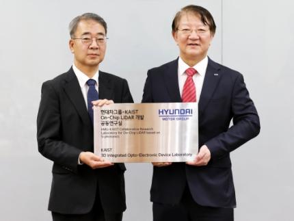 KAIST to begin Joint Research to Develop Next-Generation LiDAR System with Hyundai Motor Group
< (From left) Jong-Soo Lee, Executive Vice President at Hyundai Motor, Sang-Yup Lee, Senior Vice President for Research at KAIST >
The ‘Hyundai Motor Group-KAIST On-Chip LiDAR Joint Research Lab’ was opened at KAIST’s main campus in Daejeon to develop LiDAR sensors for advanced autonomous vehicles.
The joint research lab aims to develop high-performance and compact on-chip sensors and new signal detection technology, which are essential in the increasingly competitive autonomous driving market. On-chip sensors, which utilize semiconductor manufacturing technology to add various functions, can reduce the size of LiDAR systems compared to conventional methods and secure price competitiveness through mass production using semiconductor fabrication processes.
The joint research lab will consist of about 30 researchers, including the Hyundai-Kia Institute of Advanced Technology Development research team and KAIST professors Sanghyeon Kim, Sangsik Kim, Wanyeong Jung, and Hamza Kurt from KAIST’s School of Electrical Engineering, and will operate for four years until 2028.
KAIST will be leading the specialized work of each research team, such as for the development of silicon optoelectronic on-chip LiDAR components, the fabrication of high-speed, high-power integrated circuits to run the LiDAR systems, and the optimization and verification of LiDAR systems.
Hyundai Motor and Kia, together with Hyundai NGV, a specialized industry-academia cooperation institution, will oversee the operation of the joint research lab and provide support such as monitoring technological trends, suggesting research directions, deriving core ideas, and recommending technologies and experts to enhance research capabilities.
A Hyundai Motor Group official said, "We believe that this cooperation between Hyundai Motor Company and Kia, the leader in autonomous driving technology, and KAIST, the home of world-class technology, will hasten the achievement of fully autonomous driving." He added, "We will do our best to enable the lab to produce tangible results.”
Professor Sanghyeon Kim said, "The LiDAR sensor, which serves as the eyes of a car, is a core technology for future autonomous vehicle development that is essential for automobile companies to internalize."
2024.02.27 View 9026
KAIST to begin Joint Research to Develop Next-Generation LiDAR System with Hyundai Motor Group
< (From left) Jong-Soo Lee, Executive Vice President at Hyundai Motor, Sang-Yup Lee, Senior Vice President for Research at KAIST >
The ‘Hyundai Motor Group-KAIST On-Chip LiDAR Joint Research Lab’ was opened at KAIST’s main campus in Daejeon to develop LiDAR sensors for advanced autonomous vehicles.
The joint research lab aims to develop high-performance and compact on-chip sensors and new signal detection technology, which are essential in the increasingly competitive autonomous driving market. On-chip sensors, which utilize semiconductor manufacturing technology to add various functions, can reduce the size of LiDAR systems compared to conventional methods and secure price competitiveness through mass production using semiconductor fabrication processes.
The joint research lab will consist of about 30 researchers, including the Hyundai-Kia Institute of Advanced Technology Development research team and KAIST professors Sanghyeon Kim, Sangsik Kim, Wanyeong Jung, and Hamza Kurt from KAIST’s School of Electrical Engineering, and will operate for four years until 2028.
KAIST will be leading the specialized work of each research team, such as for the development of silicon optoelectronic on-chip LiDAR components, the fabrication of high-speed, high-power integrated circuits to run the LiDAR systems, and the optimization and verification of LiDAR systems.
Hyundai Motor and Kia, together with Hyundai NGV, a specialized industry-academia cooperation institution, will oversee the operation of the joint research lab and provide support such as monitoring technological trends, suggesting research directions, deriving core ideas, and recommending technologies and experts to enhance research capabilities.
A Hyundai Motor Group official said, "We believe that this cooperation between Hyundai Motor Company and Kia, the leader in autonomous driving technology, and KAIST, the home of world-class technology, will hasten the achievement of fully autonomous driving." He added, "We will do our best to enable the lab to produce tangible results.”
Professor Sanghyeon Kim said, "The LiDAR sensor, which serves as the eyes of a car, is a core technology for future autonomous vehicle development that is essential for automobile companies to internalize."
2024.02.27 View 9026 -
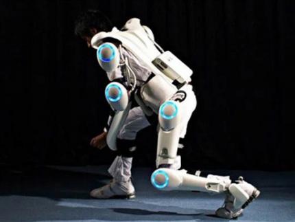 KAIST Research Team Develops Sweat-Resistant Wearable Robot Sensor
New electromyography (EMG) sensor technology that allows the long-term stable control of wearable robots and is not affected by the wearer’s sweat and dead skin has gained attention recently. Wearable robots are devices used across a variety of rehabilitation treatments for the elderly and patients recovering from stroke or trauma.
A joint research team led by Professor Jae-Woong Jung from the KAIST School of Electrical Engineering (EE) and Professor Jung Kim from the KAIST Department of Mechanical Engineering (ME) announced on January 23rd that they have successfully developed a stretchable and adhesive microneedle sensor that can electrically sense physiological signals at a high level without being affected by the state of the user’s skin.
For wearable robots to recognize the intentions behind human movement for their use in rehabilitation treatment, they require a wearable electrophysiological sensor that gives precise EMG measurements. However, existing sensors often show deteriorating signal quality over time and are greatly affected by the user’s skin conditions. Furthermore, the sensor’s higher mechanical hardness causes noise since the contact surface is unable to keep up with the deformation of the skin. These shortcomings limit the reliable, long-term control of wearable robots.
< Figure 1. Design and working concept of the Stretchable microNeedle Adhesive Patch (SNAP). (A) Schematic illustration showing the overall system configuration and application of SNAP. (B) Exploded view schematic diagram of a SNAP, consisting of stretchable serpentine interconnects, Au-coated Si microneedle, and ECA made of Ag flakes–silicone composite. (C) Optical images showing high mechanical compliance of SNAP. >
However, the recently developed technology is expected to allow long-term and high-quality EMG measurements as it uses a stretchable and adhesive conducting substrate integrated with microneedle arrays that can easily penetrate the stratum corneum without causing discomfort. Through its excellent performance, the sensor is anticipated to be able to stably control wearable robots over a long period of time regardless of the wearer’s changing skin conditions and without the need for a preparation step that removes sweat and dead cells from the surface of their skin.
The research team created a stretchable and adhesive microneedle sensor by integrating microneedles into a soft silicon polymer substrate. The hard microneedles penetrate through the stratum corneum, which has high electrical resistance. As a result, the sensor can effectively lower contact resistance with the skin and obtain high-quality electrophysiological signals regardless of contamination. At the same time, the soft and adhesive conducting substrate can adapt to the skin’s surface that stretches with the wearer’s movement, providing a comfortable fit and minimizing noise caused by movement.
< Figure 2. Demonstration of the wireless Stretchable microNeedle Adhesive Patch (SNAP) system as an Human-machine interfaces (HMI) for closed-loop control of an exoskeleton robot. (A) Illustration depicting the system architecture and control strategy of an exoskeleton robot. (B) The hardware configuration of the pneumatic back support exoskeleton system. (C) Comparison of root mean square (RMS) of electromyography (EMG) with and without robotic assistance of pretreated skin and non-pretreated skin. >
To verify the usability of the new patch, the research team conducted a motion assistance experiment using a wearable robot. They attached the microneedle patch on a user’s leg, where it could sense the electrical signals generated by the muscle. The sensor then sent the detected intention to a wearable robot, allowing the robot to help the wearer lift a heavy object more easily.
Professor Jae-Woong Jung, who led the research, said, “The developed stretchable and adhesive microneedle sensor can stability detect EMG signals without being affected by the state of a user’s skin. Through this, we will be able to control wearable robots with higher precision and stability, which will help the rehabilitation of patients who use robots.”
The results of this research, written by co-first authors Heesoo Kim and Juhyun Lee, who are both Ph.D. candidates in the KAIST School of EE, were published in Science Advances on January 17th under the title “Skin-preparation-free, stretchable microneedle adhesive patches for reliable electrophysiological sensing and exoskeleton robot control”.
This research was supported by the Bio-signal Sensor Integrated Technology Development Project by the National Research Foundation of Korea, the Electronic Medicinal Technology Development Project, and the Step 4 BK21 Project.
2024.01.30 View 7308
KAIST Research Team Develops Sweat-Resistant Wearable Robot Sensor
New electromyography (EMG) sensor technology that allows the long-term stable control of wearable robots and is not affected by the wearer’s sweat and dead skin has gained attention recently. Wearable robots are devices used across a variety of rehabilitation treatments for the elderly and patients recovering from stroke or trauma.
A joint research team led by Professor Jae-Woong Jung from the KAIST School of Electrical Engineering (EE) and Professor Jung Kim from the KAIST Department of Mechanical Engineering (ME) announced on January 23rd that they have successfully developed a stretchable and adhesive microneedle sensor that can electrically sense physiological signals at a high level without being affected by the state of the user’s skin.
For wearable robots to recognize the intentions behind human movement for their use in rehabilitation treatment, they require a wearable electrophysiological sensor that gives precise EMG measurements. However, existing sensors often show deteriorating signal quality over time and are greatly affected by the user’s skin conditions. Furthermore, the sensor’s higher mechanical hardness causes noise since the contact surface is unable to keep up with the deformation of the skin. These shortcomings limit the reliable, long-term control of wearable robots.
< Figure 1. Design and working concept of the Stretchable microNeedle Adhesive Patch (SNAP). (A) Schematic illustration showing the overall system configuration and application of SNAP. (B) Exploded view schematic diagram of a SNAP, consisting of stretchable serpentine interconnects, Au-coated Si microneedle, and ECA made of Ag flakes–silicone composite. (C) Optical images showing high mechanical compliance of SNAP. >
However, the recently developed technology is expected to allow long-term and high-quality EMG measurements as it uses a stretchable and adhesive conducting substrate integrated with microneedle arrays that can easily penetrate the stratum corneum without causing discomfort. Through its excellent performance, the sensor is anticipated to be able to stably control wearable robots over a long period of time regardless of the wearer’s changing skin conditions and without the need for a preparation step that removes sweat and dead cells from the surface of their skin.
The research team created a stretchable and adhesive microneedle sensor by integrating microneedles into a soft silicon polymer substrate. The hard microneedles penetrate through the stratum corneum, which has high electrical resistance. As a result, the sensor can effectively lower contact resistance with the skin and obtain high-quality electrophysiological signals regardless of contamination. At the same time, the soft and adhesive conducting substrate can adapt to the skin’s surface that stretches with the wearer’s movement, providing a comfortable fit and minimizing noise caused by movement.
< Figure 2. Demonstration of the wireless Stretchable microNeedle Adhesive Patch (SNAP) system as an Human-machine interfaces (HMI) for closed-loop control of an exoskeleton robot. (A) Illustration depicting the system architecture and control strategy of an exoskeleton robot. (B) The hardware configuration of the pneumatic back support exoskeleton system. (C) Comparison of root mean square (RMS) of electromyography (EMG) with and without robotic assistance of pretreated skin and non-pretreated skin. >
To verify the usability of the new patch, the research team conducted a motion assistance experiment using a wearable robot. They attached the microneedle patch on a user’s leg, where it could sense the electrical signals generated by the muscle. The sensor then sent the detected intention to a wearable robot, allowing the robot to help the wearer lift a heavy object more easily.
Professor Jae-Woong Jung, who led the research, said, “The developed stretchable and adhesive microneedle sensor can stability detect EMG signals without being affected by the state of a user’s skin. Through this, we will be able to control wearable robots with higher precision and stability, which will help the rehabilitation of patients who use robots.”
The results of this research, written by co-first authors Heesoo Kim and Juhyun Lee, who are both Ph.D. candidates in the KAIST School of EE, were published in Science Advances on January 17th under the title “Skin-preparation-free, stretchable microneedle adhesive patches for reliable electrophysiological sensing and exoskeleton robot control”.
This research was supported by the Bio-signal Sensor Integrated Technology Development Project by the National Research Foundation of Korea, the Electronic Medicinal Technology Development Project, and the Step 4 BK21 Project.
2024.01.30 View 7308 -
 KAIST and Hyundai Motors Collaborate to Develop Ultra-Fast Hydrogen Leak Detection within 0.6 Seconds
Recently, as the spread of eco-friendly hydrogen cars increases, the importance of hydrogen sensors is also on the rise. In particular, achieving technology to detect hydrogen leaks within one second remains a challenging task. Accordingly, the development of the world's first hydrogen sensor that meets the performance standards of the U.S. Department of Energy has become a hot topic.
A team at KAIST led by Dr. Min-Seung Jo from Professor Jun-Bo Yoon's team in the Department of Electrical and Electronic Engineering has successfully achieved all of its desired performance indicators, meeting globally recognized standards through collaboration with the Electromagnetic Energy Materials Research Team at Hyundai Motor Company's Basic Materials Research Center and Professor Min-Ho Seo of Pusan National University. On January 10th, the research group announced that the world's first hydrogen sensor with a speed of less than 0.6 seconds had been developed.
In order to secure faster and more stable hydrogen detection technology than existing commercialized hydrogen sensors, the KAIST team began developing a next-generation hydrogen sensor in 2021 together with Hyundai Motor Company, and succeeded after two years of development.
< Figure 1. (Left) The conceptual drawing of the structure of the coplanar heater-integrated hydrogen sensor. Pd nanowire is stably suspended in the air even with its thickness of 20 nm. (Right) A graph of hydrogen sensor performance operating within 0.6 seconds for hydrogen at a concentration of 0.1 to 4% >
Existing hydrogen sensor research has mainly focused on sensing materials, such as catalytic treatments or the alloying of palladium (Pd) materials, which are widely used in hydrogen sensors. Although these studies showed excellent performance with certain performance indicators, they did not meet all of the desired performance indicators and commercialization was limited due to the difficulty of batch processing.
To overcome this, the research team developed a sensor that satisfied all of the performance indicators by combining independent micro/nano structure design and process technology based on pure palladium materials. In addition, considering future mass production, pure metal materials with fewer material restrictions were used rather than synthetic materials, and a next-generation hydrogen sensor was developed that can be mass-produced based on a semiconductor batch process.
The developed device is a differential coplanar device in which the heater and sensing materials are integrated side by side on the same plane to overcome the uneven temperature distribution of existing gas sensors, which have a structure where the heater, insulating layer, and sensing materials are stacked vertically. The palladium nanomaterial, which is a sensing material, has a completely floating structure and is exposed to air from beneath, maximizing the reaction area with a gas to ensure a fast reaction speed. In addition, the palladium sensing material operates at a uniform temperature throughout the entire area, and the research team was able to secure a fast operation speed, wide sensing concentration, and temperature/humidity insensitivity by accurately controlling temperature-sensitive sensing performance.
< Figure 2. Electron microscopy of the coplanar heater-integrated hydrogen sensor (left) Photo of the entire device (top right) Pd nanowire suspended in the air (bottom right) Cross section of Pd nanowire >
The research team packaged the fabricated device with a Bluetooth module to create an integrated module that wirelessly detects hydrogen leaks within one second and then verified its performance. Unlike existing high-performance optical hydrogen sensors, this one is highly portable and can be used in a variety of applications where hydrogen energy is used.
Dr. Min-Seung Jo, who led the research, said, “The results of this research are of significant value as they not only operate at high speeds by exceeding the performance limits of existing hydrogen sensors, but also secure the reliability and stability necessary for actual use, and can be used in various places such as automobiles, hydrogen charging stations, and homes.” He also revealed his future plans, saying, “Through the commercialization of this hydrogen sensor technology, I would like to contribute to advancing the safe and eco-friendly use of hydrogen energy.”
< Figure 3. (Left) Real-time hydrogen detection results from the coplanar heater-integrated hydrogen sensor integrated and packaged in wireless communication and an app for mobile phone. (Middle) LED blinking cycle control in accordance with the hydrogen concentration level. (Right) Results of performance confirmation of the detection within 1 second in a real-time hydrogen leak demo >
The research team is currently working with Hyundai Motor Company to manufacture the device on a wafer scale and then mount it on a vehicle module to further verify detection and durability performance.
This research, conducted by Dr. Min-Seung Jo as the first author, has three patent applications filed in the U.S. and Korea, and was published in the renowned international academic journal 'ACS Nano'. (Paper title: Ultrafast (∼0.6 s), Robust, and Highly Linear Hydrogen Detection up to 10% Using Fully Suspended Pure Pd Nanowire). (Impact Factor: 18.087). ( https://pubs.acs.org/doi/10.1021/acsnano.3c06806?fig=fig1&ref=pdf )
The research was conducted through support from the National Research Foundation of Korea's Nano and Materials Technology Development Project and support and joint development efforts from Hyundai Motor Company's Basic Materials Research Center.
2024.01.25 View 5824
KAIST and Hyundai Motors Collaborate to Develop Ultra-Fast Hydrogen Leak Detection within 0.6 Seconds
Recently, as the spread of eco-friendly hydrogen cars increases, the importance of hydrogen sensors is also on the rise. In particular, achieving technology to detect hydrogen leaks within one second remains a challenging task. Accordingly, the development of the world's first hydrogen sensor that meets the performance standards of the U.S. Department of Energy has become a hot topic.
A team at KAIST led by Dr. Min-Seung Jo from Professor Jun-Bo Yoon's team in the Department of Electrical and Electronic Engineering has successfully achieved all of its desired performance indicators, meeting globally recognized standards through collaboration with the Electromagnetic Energy Materials Research Team at Hyundai Motor Company's Basic Materials Research Center and Professor Min-Ho Seo of Pusan National University. On January 10th, the research group announced that the world's first hydrogen sensor with a speed of less than 0.6 seconds had been developed.
In order to secure faster and more stable hydrogen detection technology than existing commercialized hydrogen sensors, the KAIST team began developing a next-generation hydrogen sensor in 2021 together with Hyundai Motor Company, and succeeded after two years of development.
< Figure 1. (Left) The conceptual drawing of the structure of the coplanar heater-integrated hydrogen sensor. Pd nanowire is stably suspended in the air even with its thickness of 20 nm. (Right) A graph of hydrogen sensor performance operating within 0.6 seconds for hydrogen at a concentration of 0.1 to 4% >
Existing hydrogen sensor research has mainly focused on sensing materials, such as catalytic treatments or the alloying of palladium (Pd) materials, which are widely used in hydrogen sensors. Although these studies showed excellent performance with certain performance indicators, they did not meet all of the desired performance indicators and commercialization was limited due to the difficulty of batch processing.
To overcome this, the research team developed a sensor that satisfied all of the performance indicators by combining independent micro/nano structure design and process technology based on pure palladium materials. In addition, considering future mass production, pure metal materials with fewer material restrictions were used rather than synthetic materials, and a next-generation hydrogen sensor was developed that can be mass-produced based on a semiconductor batch process.
The developed device is a differential coplanar device in which the heater and sensing materials are integrated side by side on the same plane to overcome the uneven temperature distribution of existing gas sensors, which have a structure where the heater, insulating layer, and sensing materials are stacked vertically. The palladium nanomaterial, which is a sensing material, has a completely floating structure and is exposed to air from beneath, maximizing the reaction area with a gas to ensure a fast reaction speed. In addition, the palladium sensing material operates at a uniform temperature throughout the entire area, and the research team was able to secure a fast operation speed, wide sensing concentration, and temperature/humidity insensitivity by accurately controlling temperature-sensitive sensing performance.
< Figure 2. Electron microscopy of the coplanar heater-integrated hydrogen sensor (left) Photo of the entire device (top right) Pd nanowire suspended in the air (bottom right) Cross section of Pd nanowire >
The research team packaged the fabricated device with a Bluetooth module to create an integrated module that wirelessly detects hydrogen leaks within one second and then verified its performance. Unlike existing high-performance optical hydrogen sensors, this one is highly portable and can be used in a variety of applications where hydrogen energy is used.
Dr. Min-Seung Jo, who led the research, said, “The results of this research are of significant value as they not only operate at high speeds by exceeding the performance limits of existing hydrogen sensors, but also secure the reliability and stability necessary for actual use, and can be used in various places such as automobiles, hydrogen charging stations, and homes.” He also revealed his future plans, saying, “Through the commercialization of this hydrogen sensor technology, I would like to contribute to advancing the safe and eco-friendly use of hydrogen energy.”
< Figure 3. (Left) Real-time hydrogen detection results from the coplanar heater-integrated hydrogen sensor integrated and packaged in wireless communication and an app for mobile phone. (Middle) LED blinking cycle control in accordance with the hydrogen concentration level. (Right) Results of performance confirmation of the detection within 1 second in a real-time hydrogen leak demo >
The research team is currently working with Hyundai Motor Company to manufacture the device on a wafer scale and then mount it on a vehicle module to further verify detection and durability performance.
This research, conducted by Dr. Min-Seung Jo as the first author, has three patent applications filed in the U.S. and Korea, and was published in the renowned international academic journal 'ACS Nano'. (Paper title: Ultrafast (∼0.6 s), Robust, and Highly Linear Hydrogen Detection up to 10% Using Fully Suspended Pure Pd Nanowire). (Impact Factor: 18.087). ( https://pubs.acs.org/doi/10.1021/acsnano.3c06806?fig=fig1&ref=pdf )
The research was conducted through support from the National Research Foundation of Korea's Nano and Materials Technology Development Project and support and joint development efforts from Hyundai Motor Company's Basic Materials Research Center.
2024.01.25 View 5824 -
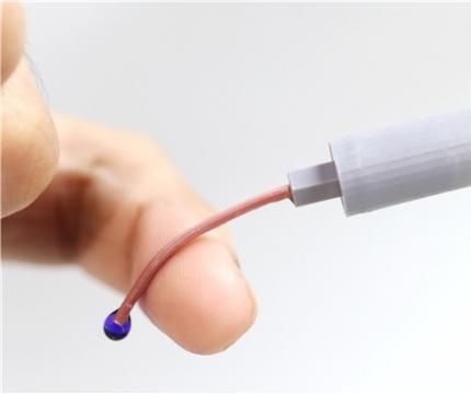 An intravenous needle that irreversibly softens via body temperature on insertion
- A joint research team at KAIST developed an intravenous (IV) needle that softens upon insertion, minimizing risk of damage to blood vessels and tissues.
- Once used, it remains soft even at room temperature, preventing accidental needle stick injuries and unethical multiple use of needle.
- A thin-film temperature sensor can be embedded with this needle, enabling real-time monitoring of the patient's core body temperature, or detection of unintended fluid leakage, during IV medication.
Intravenous (IV) injection is a method commonly used in patient’s treatment worldwide as it induces rapid effects and allows treatment through continuous administration of medication by directly injecting drugs into the blood vessel. However, medical IV needles, made of hard materials such as stainless steel or plastic which do not mechanically match the soft biological tissues of the body, can cause critical problems in healthcare settings, starting from minor tissue damages in the injection sites to serious inflammations.
The structure and dexterity of rigid medical IV devices also enable unethical reuse of needles for reduction of injection costs, leading to transmission of deadly blood-borne disease infections such as human immunodeficiency virus (HIV) and hepatitis B/C viruses. Furthermore, unintended needlestick injuries are frequently occurring in medical settings worldwide, that are viable sources of such infections, with IV needles having the greatest susceptibility of being the medium of transmissible diseases. For these reasons, the World Health Organization (WHO) in 2015 launched a policy on safe injection practices to encourage the development and use of “smart” syringes that have features to prevent re-use, after a tremendous increase in the number of deadly infectious disease worldwide due to medical-sharps related issues.
KAIST announced on the 13th that Professor Jae-Woong Jeong and his research team of its School of Electrical Engineering succeeded in developing the Phase-Convertible, Adapting and non-REusable (P-CARE) needle with variable stiffness that can improve patient health and ensure the safety of medical staff through convergent joint research with another team led by Professor Won-Il Jeong of the Graduate School of Medical Sciences.
The new technology is expected to allow patients to move without worrying about pain at the injection site as it reduces the risk of damage to the wall of the blood vessel as patients receive IV medication. This is possible with the needle’s stiffness-tunable characteristics which will make it soft and flexible upon insertion into the body due to increased temperature, adapting to the movement of thin-walled vein. It is also expected to prevent blood-borne disease infections caused by accidental needlestick injuries or unethical re-using of syringes as the deformed needle remains perpetually soft even after it is retracted from the injection site.
The results of this research, in which Karen-Christian Agno, a doctoral researcher of the School of Electrical Engineering at and Dr. Keungmo Yang of the Graduate School of Medical Sciences participated as co-first authors, was published in Nature Biomedical Engineering on October 30. (Paper title: A temperature-responsive intravenous needle that irreversibly softens on insertion)
< Figure 1. Disposable variable stiffness intravenous needle. (a) Conceptual illustration of the key features of the P-CARE needle whose mechanical properties can be changed by body temperature, (b) Photograph of commonly used IV access devices and the P-CARE needle, (c) Performance of common IV access devices and the P-CARE needle >
“We’ve developed this special needle using advanced materials and micro/nano engineering techniques, and it can solve many global problems related to conventional medical needles used in healthcare worldwide”, said Jae-Woong Jeong, Ph.D., an associate professor of Electrical Engineering at KAIST and a lead senior author of the study.
The softening IV needle created by the research team is made up of liquid metal gallium that forms the hollow, mechanical needle frame encapsulated within an ultra-soft silicone material. In its solid state, gallium has sufficient hardness that enables puncturing of soft biological tissues. However, gallium melts when it is exposed to body temperature upon insertion, and changes it into a soft state like the surrounding tissue, enabling stable delivery of the drug without damaging blood vessels. Once used, a needle remains soft even at room temperature due to the supercooling phenomenon of gallium, fundamentally preventing needlestick accidents and reuse problems.
Biocompatibility of the softening IV needle was validated through in vivo studies in mice. The studies showed that implanted needles caused significantly less inflammation relative to the standard IV access devices of similar size made of metal needles or plastic catheters. The study also confirmed the new needle was able to deliver medications as reliably as commercial injection needles.
< Photo 1. Photo of the P-CARE needle that softens with body temperature. >
Researchers also showed possibility of integrating a customized ultra-thin temperature sensor with the softening IV needle to measure the on-site temperature which can further enhance patient’s well-being. The single assembly of sensor-needle device can be used to monitor the core body temperature, or even detect if there is a fluid leakage on-site during indwelling use, eliminating the need for additional medical tools or procedures to provide the patients with better health care services.
The researchers believe that this transformative IV needle can open new opportunities for wide range of applications particularly in clinical setups, in terms of redesigning other medical needles and sharp medical tools to reduce muscle tissue injury during indwelling use. The softening IV needle may become even more valuable in the present times as there is an estimated 16 billion medical injections administered annually in a global scale, yet not all needles are disposed of properly, based on a 2018 WHO report.
< Figure 2. Biocompatibility test for P-CARE needle: Images of H&E stained histology (the area inside the dashed box on the left is provided in an expanded view in the right), TUNEL staining (green), DAPI staining of nuclei (blue) and co-staining (TUNEL and DAPI) of muscle tissue from different organs. >
< Figure 3. Conceptual images of potential utilization for temperature monitoring function of P-CARE needle integrated with a temperature sensor. >
(a) Schematic diagram of injecting a drug through intravenous injection into the abdomen of a laboratory mouse (b) Change of body temperature upon injection of drug (c) Conceptual illustration of normal intravenous drug injection (top) and fluid leakage (bottom) (d) Comparison of body temperature during normal drug injection and fluid leakage: when the fluid leak occur due to incorrect insertion, a sudden drop of temperature is detected.
This work was supported by grants from the National Research Foundation of Korea (NRF) funded by the Ministry of Science and ICT.
2023.11.13 View 8650
An intravenous needle that irreversibly softens via body temperature on insertion
- A joint research team at KAIST developed an intravenous (IV) needle that softens upon insertion, minimizing risk of damage to blood vessels and tissues.
- Once used, it remains soft even at room temperature, preventing accidental needle stick injuries and unethical multiple use of needle.
- A thin-film temperature sensor can be embedded with this needle, enabling real-time monitoring of the patient's core body temperature, or detection of unintended fluid leakage, during IV medication.
Intravenous (IV) injection is a method commonly used in patient’s treatment worldwide as it induces rapid effects and allows treatment through continuous administration of medication by directly injecting drugs into the blood vessel. However, medical IV needles, made of hard materials such as stainless steel or plastic which do not mechanically match the soft biological tissues of the body, can cause critical problems in healthcare settings, starting from minor tissue damages in the injection sites to serious inflammations.
The structure and dexterity of rigid medical IV devices also enable unethical reuse of needles for reduction of injection costs, leading to transmission of deadly blood-borne disease infections such as human immunodeficiency virus (HIV) and hepatitis B/C viruses. Furthermore, unintended needlestick injuries are frequently occurring in medical settings worldwide, that are viable sources of such infections, with IV needles having the greatest susceptibility of being the medium of transmissible diseases. For these reasons, the World Health Organization (WHO) in 2015 launched a policy on safe injection practices to encourage the development and use of “smart” syringes that have features to prevent re-use, after a tremendous increase in the number of deadly infectious disease worldwide due to medical-sharps related issues.
KAIST announced on the 13th that Professor Jae-Woong Jeong and his research team of its School of Electrical Engineering succeeded in developing the Phase-Convertible, Adapting and non-REusable (P-CARE) needle with variable stiffness that can improve patient health and ensure the safety of medical staff through convergent joint research with another team led by Professor Won-Il Jeong of the Graduate School of Medical Sciences.
The new technology is expected to allow patients to move without worrying about pain at the injection site as it reduces the risk of damage to the wall of the blood vessel as patients receive IV medication. This is possible with the needle’s stiffness-tunable characteristics which will make it soft and flexible upon insertion into the body due to increased temperature, adapting to the movement of thin-walled vein. It is also expected to prevent blood-borne disease infections caused by accidental needlestick injuries or unethical re-using of syringes as the deformed needle remains perpetually soft even after it is retracted from the injection site.
The results of this research, in which Karen-Christian Agno, a doctoral researcher of the School of Electrical Engineering at and Dr. Keungmo Yang of the Graduate School of Medical Sciences participated as co-first authors, was published in Nature Biomedical Engineering on October 30. (Paper title: A temperature-responsive intravenous needle that irreversibly softens on insertion)
< Figure 1. Disposable variable stiffness intravenous needle. (a) Conceptual illustration of the key features of the P-CARE needle whose mechanical properties can be changed by body temperature, (b) Photograph of commonly used IV access devices and the P-CARE needle, (c) Performance of common IV access devices and the P-CARE needle >
“We’ve developed this special needle using advanced materials and micro/nano engineering techniques, and it can solve many global problems related to conventional medical needles used in healthcare worldwide”, said Jae-Woong Jeong, Ph.D., an associate professor of Electrical Engineering at KAIST and a lead senior author of the study.
The softening IV needle created by the research team is made up of liquid metal gallium that forms the hollow, mechanical needle frame encapsulated within an ultra-soft silicone material. In its solid state, gallium has sufficient hardness that enables puncturing of soft biological tissues. However, gallium melts when it is exposed to body temperature upon insertion, and changes it into a soft state like the surrounding tissue, enabling stable delivery of the drug without damaging blood vessels. Once used, a needle remains soft even at room temperature due to the supercooling phenomenon of gallium, fundamentally preventing needlestick accidents and reuse problems.
Biocompatibility of the softening IV needle was validated through in vivo studies in mice. The studies showed that implanted needles caused significantly less inflammation relative to the standard IV access devices of similar size made of metal needles or plastic catheters. The study also confirmed the new needle was able to deliver medications as reliably as commercial injection needles.
< Photo 1. Photo of the P-CARE needle that softens with body temperature. >
Researchers also showed possibility of integrating a customized ultra-thin temperature sensor with the softening IV needle to measure the on-site temperature which can further enhance patient’s well-being. The single assembly of sensor-needle device can be used to monitor the core body temperature, or even detect if there is a fluid leakage on-site during indwelling use, eliminating the need for additional medical tools or procedures to provide the patients with better health care services.
The researchers believe that this transformative IV needle can open new opportunities for wide range of applications particularly in clinical setups, in terms of redesigning other medical needles and sharp medical tools to reduce muscle tissue injury during indwelling use. The softening IV needle may become even more valuable in the present times as there is an estimated 16 billion medical injections administered annually in a global scale, yet not all needles are disposed of properly, based on a 2018 WHO report.
< Figure 2. Biocompatibility test for P-CARE needle: Images of H&E stained histology (the area inside the dashed box on the left is provided in an expanded view in the right), TUNEL staining (green), DAPI staining of nuclei (blue) and co-staining (TUNEL and DAPI) of muscle tissue from different organs. >
< Figure 3. Conceptual images of potential utilization for temperature monitoring function of P-CARE needle integrated with a temperature sensor. >
(a) Schematic diagram of injecting a drug through intravenous injection into the abdomen of a laboratory mouse (b) Change of body temperature upon injection of drug (c) Conceptual illustration of normal intravenous drug injection (top) and fluid leakage (bottom) (d) Comparison of body temperature during normal drug injection and fluid leakage: when the fluid leak occur due to incorrect insertion, a sudden drop of temperature is detected.
This work was supported by grants from the National Research Foundation of Korea (NRF) funded by the Ministry of Science and ICT.
2023.11.13 View 8650 -
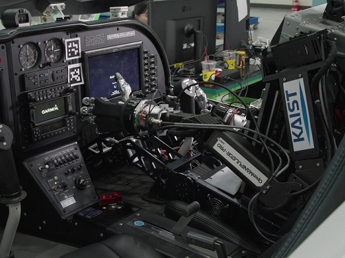 KAIST Research Team Develops World’s First Humanoid Pilot, PIBOT
In the Spring of last year, the legendary, fictional pilot “Maverick” flew his plane in the film “Top Gun: Maverick” that drew crowds to theatres around the world. This year, the appearance of a humanoid pilot, PIBOT, has stolen the spotlight at KAIST.
< Photo 1. Humanoid pilot robot, PIBOT >
A KAIST research team has developed a humanoid robot that can understand manuals written in natural language and fly a plane on its own. The team also announced their plans to commercialize the humanoid pilot.
< Photo 2. PIBOT on flight simulator (view from above) >
The project was led by KAIST Professor David Hyunchul Shim, and was conducted as a joint research project with Professors Jaegul Choo, Kuk-Jin Yoon, and Min Jun Kim. The study was supported by Future Challenge Funding under the project title, “Development of Human-like Pilot Robot based on Natural Language Processing”. The team utilized AI and robotics technologies, and demonstrated that the humanoid could sit itself in a real cockpit and operate the various pieces of equipment without modifying any part of the aircraft. This is a fundamental difference that distinguishes this technology from existing autopilot functions or unmanned aircrafts.
< Photo 3. PIBOT operating a flight simulator (side) >
The KAIST team’s humanoid pilot is still under development but it can already remember Jeppeson charts from all around the world, which is impossible for human pilots to do, and fly without error. In particular, it can make use of recent ChatGPT technology to remember the full Quick Reference Handbook (QRF) and respond immediately to various situations, as well as calculate safe routes in real time based on the flight status of the aircraft, with emergency response times quicker than human pilots.
Furthermore, while existing robots usually carry out repeated motions in a fixed position, PIBOT can analyze the state of the cockpit as well as the situation outside the aircraft using an embedded camera. PIBOT can accurately control the various switches in the cockpit and, using high-precision control technology, it can accurately control its robotic arms and hands even during harsh turbulence.
< Photo 4. PIBOT on-board KLA-100, Korea’s first light aircraft >
The humanoid pilot is currently capable of carrying out all operations from starting the aircraft to taxiing, takeoff and landing, cruising, and cycling using a flight control simulator. The research team plans to use the humanoid pilot to fly a real-life light aircraft to verify its abilities. Prof. Shim explained, “Humanoid pilot robots do not require the modification of existing aircrafts and can be applied immediately to automated flights. They are therefore highly applicable and practical. We expect them to be applied into various other vehicles like cars and military trucks since they can control a wide range of equipment. They will particularly be particularly helpful in situations where military resources are severely depleted.”
This research was supported by Future Challenge Funding (total: 5.7 bn KRW) from the Agency for Defense Development. The project started in 2022 as a joint research project by Prof. David Hyunchul Shim (chief of research) from the KAIST School of Electrical Engineering (EE), Prof. Jaegul Choo from the Kim Jaechul Graduate School of AI at KAIST, Prof. Kuk-Jin Yoon from the KAIST Department of Mechanical Engineering, and Prof. Min Jun Kim from the KAIST School of EE. The project is to be completed by 2026 and the involved researchers are also considering commercialization strategies for both military and civil use.
2023.08.03 View 14093
KAIST Research Team Develops World’s First Humanoid Pilot, PIBOT
In the Spring of last year, the legendary, fictional pilot “Maverick” flew his plane in the film “Top Gun: Maverick” that drew crowds to theatres around the world. This year, the appearance of a humanoid pilot, PIBOT, has stolen the spotlight at KAIST.
< Photo 1. Humanoid pilot robot, PIBOT >
A KAIST research team has developed a humanoid robot that can understand manuals written in natural language and fly a plane on its own. The team also announced their plans to commercialize the humanoid pilot.
< Photo 2. PIBOT on flight simulator (view from above) >
The project was led by KAIST Professor David Hyunchul Shim, and was conducted as a joint research project with Professors Jaegul Choo, Kuk-Jin Yoon, and Min Jun Kim. The study was supported by Future Challenge Funding under the project title, “Development of Human-like Pilot Robot based on Natural Language Processing”. The team utilized AI and robotics technologies, and demonstrated that the humanoid could sit itself in a real cockpit and operate the various pieces of equipment without modifying any part of the aircraft. This is a fundamental difference that distinguishes this technology from existing autopilot functions or unmanned aircrafts.
< Photo 3. PIBOT operating a flight simulator (side) >
The KAIST team’s humanoid pilot is still under development but it can already remember Jeppeson charts from all around the world, which is impossible for human pilots to do, and fly without error. In particular, it can make use of recent ChatGPT technology to remember the full Quick Reference Handbook (QRF) and respond immediately to various situations, as well as calculate safe routes in real time based on the flight status of the aircraft, with emergency response times quicker than human pilots.
Furthermore, while existing robots usually carry out repeated motions in a fixed position, PIBOT can analyze the state of the cockpit as well as the situation outside the aircraft using an embedded camera. PIBOT can accurately control the various switches in the cockpit and, using high-precision control technology, it can accurately control its robotic arms and hands even during harsh turbulence.
< Photo 4. PIBOT on-board KLA-100, Korea’s first light aircraft >
The humanoid pilot is currently capable of carrying out all operations from starting the aircraft to taxiing, takeoff and landing, cruising, and cycling using a flight control simulator. The research team plans to use the humanoid pilot to fly a real-life light aircraft to verify its abilities. Prof. Shim explained, “Humanoid pilot robots do not require the modification of existing aircrafts and can be applied immediately to automated flights. They are therefore highly applicable and practical. We expect them to be applied into various other vehicles like cars and military trucks since they can control a wide range of equipment. They will particularly be particularly helpful in situations where military resources are severely depleted.”
This research was supported by Future Challenge Funding (total: 5.7 bn KRW) from the Agency for Defense Development. The project started in 2022 as a joint research project by Prof. David Hyunchul Shim (chief of research) from the KAIST School of Electrical Engineering (EE), Prof. Jaegul Choo from the Kim Jaechul Graduate School of AI at KAIST, Prof. Kuk-Jin Yoon from the KAIST Department of Mechanical Engineering, and Prof. Min Jun Kim from the KAIST School of EE. The project is to be completed by 2026 and the involved researchers are also considering commercialization strategies for both military and civil use.
2023.08.03 View 14093 -
 A KAIST research team develops a washable, transparent, and flexible OLED with MXene nanotechnology
Transparent and flexible displays, which have received a lot of attention in various fields including automobile displays, bio-healthcare, military, and fashion, are in fact known to break easily when experiencing small deformations. To solve this problem, active research is being conducted on many transparent and flexible conductive materials such as carbon nanotubes, graphene, silver nanowires, and conductive polymers.
On June 13, a joint research team led by Professor Kyung Cheol Choi from the KAIST School of Electrical Engineering and Dr. Yonghee Lee from the National Nano Fab Center (NNFC) announced the successful development of a water-resistant, transparent, and flexible OLED using MXene nanotechnology. The material can emit and transmit light even when exposed to water.
MXene is a 2D material with high electrical conductivity and optical transmittance, and it can be produced on a large scale through solution processes. However, despite these attractive properties, MXene’s applications were limited as a long-term electrical device due to its electrical properties being degraded easily by atmospheric moisture and water. The material was therefore unable to be systemized into the form of a matrix that can display information.
Professor Choi’s research team used an encapsulation tactic that can protect materials from oxidation caused by moisture and oxygen to develop a MXene-based OLED with a long lifespan and high stability against external environmental factors. The research team first focused on analyzing the degradation mechanism of MXene’s electrical conductivity, and then concentrated on designing an encapsulation membrane. The team blocked moisture and provided flexibility through residual stress offset, ultimately producing a double-layered encapsulation membrane. In addition, a thin plastic film with a thickness of a few micrometers was attached to the top layer to allow washing in water without degradation.
< Figure 1. (a) Transparent passive-matrix display made of MXene-based OLED, (b) Cross-sectional image of MXene-based OLED observed by transmission electron microscope (TEM), (c) Electro-optical characteristic graph of red, green, and blue MXene-based OLED >
Through this study, the research team developed a MXene-based red(R)/green(G)/blue(B) OLED that emits a brightness of over 1,000 cd/m2 that is detectable by the naked eye even under sunlight, thereby meeting the conditions for outdoor displays. As for the red MXene-based OLED, the researchers confirmed a standby storage life of 2,000 hours (under 70% luminescence), a standby operation life of 1,500 hours (under 60% luminescence), and a flexibility withstanding 1,000 cycles under a low curvature of under 1.5mm. In addition, they showed that its performance was maintained even after six hours of immersion under water (under 80% luminescence). Furthermore, a patterning technique was used to produce the MXene-based OLED in the form of a passive matrix, and the team demonstrated its use as a transparent display by displaying letters and shapes.
Ph.D. candidate So Yeong Jeong, who led this study, said, “To improve the reliability of MXene OLED, we focused on producing an adequate encapsulation structure and a suitable process design.” She added, “By producing a matrix-type MXene OLED and displaying simple letters and shapes, we have laid the foundations for MXene’s application in the field of transparent displays.”
< Image 1. Cover of ACS Nano Front Cover (Conceptual diagram of MXene-based OLED display) >
Professor Choi said, “This research will become the guideline for applying MXene in electrical devices, but we expect for it to also be applied in other fields that require flexible and transparent displays like automobiles, fashion, and functional clothing. And to widen the gap with China’s OLED technology, these new OLED convergence technologies must continue to be developed.”
This research was supported by the National Research Foundation of Korea and funded by the Ministry of Science and ICT, Korea. It was published as a front cover story of ACS Nano under the title, “Highly Air-Stable, Flexible, and Water-Resistive 2D Titanium Carbide MXene-Based RGB Organic Light-Emitting Diode Displays for Transparent Free-Form Electronics” on June 13.
2023.07.10 View 6716
A KAIST research team develops a washable, transparent, and flexible OLED with MXene nanotechnology
Transparent and flexible displays, which have received a lot of attention in various fields including automobile displays, bio-healthcare, military, and fashion, are in fact known to break easily when experiencing small deformations. To solve this problem, active research is being conducted on many transparent and flexible conductive materials such as carbon nanotubes, graphene, silver nanowires, and conductive polymers.
On June 13, a joint research team led by Professor Kyung Cheol Choi from the KAIST School of Electrical Engineering and Dr. Yonghee Lee from the National Nano Fab Center (NNFC) announced the successful development of a water-resistant, transparent, and flexible OLED using MXene nanotechnology. The material can emit and transmit light even when exposed to water.
MXene is a 2D material with high electrical conductivity and optical transmittance, and it can be produced on a large scale through solution processes. However, despite these attractive properties, MXene’s applications were limited as a long-term electrical device due to its electrical properties being degraded easily by atmospheric moisture and water. The material was therefore unable to be systemized into the form of a matrix that can display information.
Professor Choi’s research team used an encapsulation tactic that can protect materials from oxidation caused by moisture and oxygen to develop a MXene-based OLED with a long lifespan and high stability against external environmental factors. The research team first focused on analyzing the degradation mechanism of MXene’s electrical conductivity, and then concentrated on designing an encapsulation membrane. The team blocked moisture and provided flexibility through residual stress offset, ultimately producing a double-layered encapsulation membrane. In addition, a thin plastic film with a thickness of a few micrometers was attached to the top layer to allow washing in water without degradation.
< Figure 1. (a) Transparent passive-matrix display made of MXene-based OLED, (b) Cross-sectional image of MXene-based OLED observed by transmission electron microscope (TEM), (c) Electro-optical characteristic graph of red, green, and blue MXene-based OLED >
Through this study, the research team developed a MXene-based red(R)/green(G)/blue(B) OLED that emits a brightness of over 1,000 cd/m2 that is detectable by the naked eye even under sunlight, thereby meeting the conditions for outdoor displays. As for the red MXene-based OLED, the researchers confirmed a standby storage life of 2,000 hours (under 70% luminescence), a standby operation life of 1,500 hours (under 60% luminescence), and a flexibility withstanding 1,000 cycles under a low curvature of under 1.5mm. In addition, they showed that its performance was maintained even after six hours of immersion under water (under 80% luminescence). Furthermore, a patterning technique was used to produce the MXene-based OLED in the form of a passive matrix, and the team demonstrated its use as a transparent display by displaying letters and shapes.
Ph.D. candidate So Yeong Jeong, who led this study, said, “To improve the reliability of MXene OLED, we focused on producing an adequate encapsulation structure and a suitable process design.” She added, “By producing a matrix-type MXene OLED and displaying simple letters and shapes, we have laid the foundations for MXene’s application in the field of transparent displays.”
< Image 1. Cover of ACS Nano Front Cover (Conceptual diagram of MXene-based OLED display) >
Professor Choi said, “This research will become the guideline for applying MXene in electrical devices, but we expect for it to also be applied in other fields that require flexible and transparent displays like automobiles, fashion, and functional clothing. And to widen the gap with China’s OLED technology, these new OLED convergence technologies must continue to be developed.”
This research was supported by the National Research Foundation of Korea and funded by the Ministry of Science and ICT, Korea. It was published as a front cover story of ACS Nano under the title, “Highly Air-Stable, Flexible, and Water-Resistive 2D Titanium Carbide MXene-Based RGB Organic Light-Emitting Diode Displays for Transparent Free-Form Electronics” on June 13.
2023.07.10 View 6716 -
 A KAIST research team develops a high-performance modular SSD system semiconductor
In recent years, there has been a rise in demand for large amounts of data to train AI models and, thus, data size has become increasingly important over time. Accordingly, solid state drives (SSDs, storage devices that use a semiconductor memory unit), which are core storage devices for data centers and cloud services, have also seen an increase in demand. However, the internal components of higher performing SSDs have become more tightly coupled, and this tightly-coupled structure limits SSD from maximized performance.
On June 15, a KAIST research team led by Professor Dongjun Kim (John Kim) from the School of Electrical Engineering (EE) announced the development of the first SSD system semiconductor structure that can increase the reading/writing performance of next generation SSDs and extend their lifespan through high-performance modular SSD systems.
Professor Kim’s team identified the limitations of the tightly-coupled structures in existing SSD designs and proposed a de-coupled structure that can maximize SSD performance by configuring an internal on-chip network specialized for flash memory. This technique utilizes on-chip network technology, which can freely send packet-based data within the chip and is often used to design non-memory system semiconductors like CPUs and GPUs. Through this, the team developed a ‘modular SSD’, which shows reduced interdependence between front-end and back-end designs, and allows their independent design and assembly.
*on-chip network: a packet-based connection structure for the internal components of system semiconductors like CPUs/GPUs. On-chip networks are one of the most critical design components for high-performing system semiconductors, and their importance grows with the size of the semiconductor chip.
Professor Kim’s team refers to the components nearer to the CPU as the front-end and the parts closer to the flash memory as back-end. They newly constructed an on-chip network specific to flash memory in order to allow data transmission between the back-end’s flash controller, proposing a de-coupled structure that can minimize performance drop.
The SSD can accelerate some functions of the flash translation layer, a critical element to drive the SSD, in order to allow flash memory to actively overcome its limitations. Another advantage of the de-coupled, modular structure is that the flash translation layer is not limited to the characteristics of specific flash memories. Instead, their front-end and back-end designs can be carried out independently. Through this, the team could produce 21-times faster response times compared to existing systems and extend SSD lifespan by 23% by also applying the DDS defect detection technique.
< Figure 1. Schematic diagram of the structure of a high-performance modular SSD system developed by Professor Dong-Jun Kim's team >
This research, conducted by first author and Ph.D. candidate Jiho Kim from the KAIST School of EE and co-author Professor Myoungsoo Jung, was presented on the 19th of June at the 50th IEEE/ACM International Symposium on Computer Architecture, the most prestigious academic conference in the field of computer architecture, held in Orlando, Florida. (Paper Title: Decoupled SSD: Rethinking SSD Architecture through Network-based Flash Controllers)
< Figure 2. Conceptual diagram of hardware acceleration through high-performance modular SSD system >
Professor Dongjun Kim, who led the research, said, “This research is significant in that it identified the structural limitations of existing SSDs, and showed that on-chip network technology based on system memory semiconductors like CPUs can drive the hardware to actively carry out the necessary actions. We expect this to contribute greatly to the next-generation high-performance SSD market.” He added, “The de-coupled architecture is a structure that can actively operate to extend devices’ lifespan. In other words, its significance is not limited to the level of performance and can, therefore, be used for various applications.”
KAIST commented that this research is also meaningful in that the results were reaped through a collaborative study between two world-renowned researchers: Professor Myeongsoo Jung, recognized in the field of computer system storage devices, and Professor Dongjun Kim, a leading researcher in computer architecture and interconnection networks.
This research was funded by the National Research Foundation of Korea, Samsung Electronics, the IC Design Education Center, and Next Generation Semiconductor Technology and Development granted by the Institute of Information & Communications Technology, Planning & Evaluation.
2023.06.23 View 7069
A KAIST research team develops a high-performance modular SSD system semiconductor
In recent years, there has been a rise in demand for large amounts of data to train AI models and, thus, data size has become increasingly important over time. Accordingly, solid state drives (SSDs, storage devices that use a semiconductor memory unit), which are core storage devices for data centers and cloud services, have also seen an increase in demand. However, the internal components of higher performing SSDs have become more tightly coupled, and this tightly-coupled structure limits SSD from maximized performance.
On June 15, a KAIST research team led by Professor Dongjun Kim (John Kim) from the School of Electrical Engineering (EE) announced the development of the first SSD system semiconductor structure that can increase the reading/writing performance of next generation SSDs and extend their lifespan through high-performance modular SSD systems.
Professor Kim’s team identified the limitations of the tightly-coupled structures in existing SSD designs and proposed a de-coupled structure that can maximize SSD performance by configuring an internal on-chip network specialized for flash memory. This technique utilizes on-chip network technology, which can freely send packet-based data within the chip and is often used to design non-memory system semiconductors like CPUs and GPUs. Through this, the team developed a ‘modular SSD’, which shows reduced interdependence between front-end and back-end designs, and allows their independent design and assembly.
*on-chip network: a packet-based connection structure for the internal components of system semiconductors like CPUs/GPUs. On-chip networks are one of the most critical design components for high-performing system semiconductors, and their importance grows with the size of the semiconductor chip.
Professor Kim’s team refers to the components nearer to the CPU as the front-end and the parts closer to the flash memory as back-end. They newly constructed an on-chip network specific to flash memory in order to allow data transmission between the back-end’s flash controller, proposing a de-coupled structure that can minimize performance drop.
The SSD can accelerate some functions of the flash translation layer, a critical element to drive the SSD, in order to allow flash memory to actively overcome its limitations. Another advantage of the de-coupled, modular structure is that the flash translation layer is not limited to the characteristics of specific flash memories. Instead, their front-end and back-end designs can be carried out independently. Through this, the team could produce 21-times faster response times compared to existing systems and extend SSD lifespan by 23% by also applying the DDS defect detection technique.
< Figure 1. Schematic diagram of the structure of a high-performance modular SSD system developed by Professor Dong-Jun Kim's team >
This research, conducted by first author and Ph.D. candidate Jiho Kim from the KAIST School of EE and co-author Professor Myoungsoo Jung, was presented on the 19th of June at the 50th IEEE/ACM International Symposium on Computer Architecture, the most prestigious academic conference in the field of computer architecture, held in Orlando, Florida. (Paper Title: Decoupled SSD: Rethinking SSD Architecture through Network-based Flash Controllers)
< Figure 2. Conceptual diagram of hardware acceleration through high-performance modular SSD system >
Professor Dongjun Kim, who led the research, said, “This research is significant in that it identified the structural limitations of existing SSDs, and showed that on-chip network technology based on system memory semiconductors like CPUs can drive the hardware to actively carry out the necessary actions. We expect this to contribute greatly to the next-generation high-performance SSD market.” He added, “The de-coupled architecture is a structure that can actively operate to extend devices’ lifespan. In other words, its significance is not limited to the level of performance and can, therefore, be used for various applications.”
KAIST commented that this research is also meaningful in that the results were reaped through a collaborative study between two world-renowned researchers: Professor Myeongsoo Jung, recognized in the field of computer system storage devices, and Professor Dongjun Kim, a leading researcher in computer architecture and interconnection networks.
This research was funded by the National Research Foundation of Korea, Samsung Electronics, the IC Design Education Center, and Next Generation Semiconductor Technology and Development granted by the Institute of Information & Communications Technology, Planning & Evaluation.
2023.06.23 View 7069 -
 A KAIST research team unveils new path for dense photonic integration
Integrated optical semiconductor (hereinafter referred to as optical semiconductor) technology is a next-generation semiconductor technology for which many researches and investments are being made worldwide because it can make complex optical systems such as LiDAR and quantum sensors and computers into a single small chip. In the existing semiconductor technology, the key was how small it was to make it in units of 5 nanometers or 2 nanometers, but increasing the degree of integration in optical semiconductor devices can be said to be a key technology that determines performance, price, and energy efficiency.
KAIST (President Kwang-Hyung Lee) announced on the 19th that a research team led by Professor Sangsik Kim of the Department of Electrical and Electronic Engineering discovered a new optical coupling mechanism that can increase the degree of integration of optical semiconductor devices by more than 100 times.
The degree of the number of elements that can be configured per chip is called the degree of integration. However, it is very difficult to increase the degree of integration of optical semiconductor devices, because crosstalk occurs between photons between adjacent devices due to the wave nature of light.
In previous studies, it was possible to reduce crosstalk of light only in specific polarizations, but in this study, the research team developed a method to increase the degree of integration even under polarization conditions, which were previously considered impossible, by discovering a new light coupling mechanism.
This study, led by Professor Sangsik Kim as a corresponding author and conducted with students he taught at Texas Tech University, was published in the international journal 'Light: Science & Applications' [IF=20.257] on June 2nd. done. (Paper title: Anisotropic leaky-like perturbation with subwavelength gratings enables zero crosstalk).
Professor Sangsik Kim said, "The interesting thing about this study is that it paradoxically eliminated the confusion through leaky waves (light tends to spread sideways), which was previously thought to increase the crosstalk." He went on to add, “If the optical coupling method using the leaky wave revealed in this study is applied, it will be possible to develop various optical semiconductor devices that are smaller and that has less noise.”
Professor Sangsik Kim is a researcher recognized for his expertise and research in optical semiconductor integration. Through his previous research, he developed an all-dielectric metamaterial that can control the degree of light spreading laterally by patterning a semiconductor structure at a size smaller than the wavelength, and proved this through experiments to improve the degree of integration of optical semiconductors. These studies were reported in ‘Nature Communications’ (Vol. 9, Article 1893, 2018) and ‘Optica’ (Vol. 7, pp. 881-887, 2020). In recognition of these achievements, Professor Kim has received the NSF Career Award from the National Science Foundation (NSF) and the Young Scientist Award from the Association of Korean-American Scientists and Engineers.
Meanwhile, this research was carried out with the support from the New Research Project of Excellence of the National Research Foundation of Korea and and the National Science Foundation of the US.
< Figure 1. Illustration depicting light propagation without crosstalk in the waveguide array of the developed metamaterial-based optical semiconductor >
2023.06.21 View 7090
A KAIST research team unveils new path for dense photonic integration
Integrated optical semiconductor (hereinafter referred to as optical semiconductor) technology is a next-generation semiconductor technology for which many researches and investments are being made worldwide because it can make complex optical systems such as LiDAR and quantum sensors and computers into a single small chip. In the existing semiconductor technology, the key was how small it was to make it in units of 5 nanometers or 2 nanometers, but increasing the degree of integration in optical semiconductor devices can be said to be a key technology that determines performance, price, and energy efficiency.
KAIST (President Kwang-Hyung Lee) announced on the 19th that a research team led by Professor Sangsik Kim of the Department of Electrical and Electronic Engineering discovered a new optical coupling mechanism that can increase the degree of integration of optical semiconductor devices by more than 100 times.
The degree of the number of elements that can be configured per chip is called the degree of integration. However, it is very difficult to increase the degree of integration of optical semiconductor devices, because crosstalk occurs between photons between adjacent devices due to the wave nature of light.
In previous studies, it was possible to reduce crosstalk of light only in specific polarizations, but in this study, the research team developed a method to increase the degree of integration even under polarization conditions, which were previously considered impossible, by discovering a new light coupling mechanism.
This study, led by Professor Sangsik Kim as a corresponding author and conducted with students he taught at Texas Tech University, was published in the international journal 'Light: Science & Applications' [IF=20.257] on June 2nd. done. (Paper title: Anisotropic leaky-like perturbation with subwavelength gratings enables zero crosstalk).
Professor Sangsik Kim said, "The interesting thing about this study is that it paradoxically eliminated the confusion through leaky waves (light tends to spread sideways), which was previously thought to increase the crosstalk." He went on to add, “If the optical coupling method using the leaky wave revealed in this study is applied, it will be possible to develop various optical semiconductor devices that are smaller and that has less noise.”
Professor Sangsik Kim is a researcher recognized for his expertise and research in optical semiconductor integration. Through his previous research, he developed an all-dielectric metamaterial that can control the degree of light spreading laterally by patterning a semiconductor structure at a size smaller than the wavelength, and proved this through experiments to improve the degree of integration of optical semiconductors. These studies were reported in ‘Nature Communications’ (Vol. 9, Article 1893, 2018) and ‘Optica’ (Vol. 7, pp. 881-887, 2020). In recognition of these achievements, Professor Kim has received the NSF Career Award from the National Science Foundation (NSF) and the Young Scientist Award from the Association of Korean-American Scientists and Engineers.
Meanwhile, this research was carried out with the support from the New Research Project of Excellence of the National Research Foundation of Korea and and the National Science Foundation of the US.
< Figure 1. Illustration depicting light propagation without crosstalk in the waveguide array of the developed metamaterial-based optical semiconductor >
2023.06.21 View 7090 -
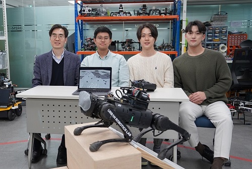 KAIST debuts “DreamWaQer” - a quadrupedal robot that can walk in the dark
- The team led by Professor Hyun Myung of the School of Electrical Engineering developed “DreamWaQ”, a deep reinforcement learning-based walking robot control technology that can walk in an atypical environment without visual and/or tactile information
- Utilization of “DreamWaQ” technology can enable mass production of various types of “DreamWaQers”
- Expected to be used in exploration of atypical environment involving unique circumstances such as disasters by fire.
A team of Korean engineering researchers has developed a quadrupedal robot technology that can climb up and down the steps and moves without falling over in uneven environments such as tree roots without the help of visual or tactile sensors even in disastrous situations in which visual confirmation is impeded due to darkness or thick smoke from the flames.
KAIST (President Kwang Hyung Lee) announced on the 29th of March that Professor Hyun Myung's research team at the Urban Robotics Lab in the School of Electrical Engineering developed a walking robot control technology that enables robust 'blind locomotion' in various atypical environments.
< (From left) Prof. Hyun Myung, Doctoral Candidates I Made Aswin Nahrendra, Byeongho Yu, and Minho Oh. In the foreground is the DreamWaQer, a quadrupedal robot equipped with DreamWaQ technology. >
The KAIST research team developed "DreamWaQ" technology, which was named so as it enables walking robots to move about even in the dark, just as a person can walk without visual help fresh out of bed and going to the bathroom in the dark. With this technology installed atop any legged robots, it will be possible to create various types of "DreamWaQers".
Existing walking robot controllers are based on kinematics and/or dynamics models. This is expressed as a model-based control method. In particular, on atypical environments like the open, uneven fields, it is necessary to obtain the feature information of the terrain more quickly in order to maintain stability as it walks. However, it has been shown to depend heavily on the cognitive ability to survey the surrounding environment.
In contrast, the controller developed by Professor Hyun Myung's research team based on deep reinforcement learning (RL) methods can quickly calculate appropriate control commands for each motor of the walking robot through data of various environments obtained from the simulator. Whereas the existing controllers that learned from simulations required a separate re-orchestration to make it work with an actual robot, this controller developed by the research team is expected to be easily applied to various walking robots because it does not require an additional tuning process.
DreamWaQ, the controller developed by the research team, is largely composed of a context estimation network that estimates the ground and robot information and a policy network that computes control commands. The context-aided estimator network estimates the ground information implicitly and the robot’s status explicitly through inertial information and joint information. This information is fed into the policy network to be used to generate optimal control commands. Both networks are learned together in the simulation.
While the context-aided estimator network is learned through supervised learning, the policy network is learned through an actor-critic architecture, a deep RL methodology. The actor network can only implicitly infer surrounding terrain information. In the simulation, the surrounding terrain information is known, and the critic, or the value network, that has the exact terrain information evaluates the policy of the actor network.
This whole learning process takes only about an hour in a GPU-enabled PC, and the actual robot is equipped with only the network of learned actors. Without looking at the surrounding terrain, it goes through the process of imagining which environment is similar to one of the various environments learned in the simulation using only the inertial sensor (IMU) inside the robot and the measurement of joint angles. If it suddenly encounters an offset, such as a staircase, it will not know until its foot touches the step, but it will quickly draw up terrain information the moment its foot touches the surface. Then the control command suitable for the estimated terrain information is transmitted to each motor, enabling rapidly adapted walking.
The DreamWaQer robot walked not only in the laboratory environment, but also in an outdoor environment around the campus with many curbs and speed bumps, and over a field with many tree roots and gravel, demonstrating its abilities by overcoming a staircase with a difference of a height that is two-thirds of its body. In addition, regardless of the environment, the research team confirmed that it was capable of stable walking ranging from a slow speed of 0.3 m/s to a rather fast speed of 1.0 m/s.
The results of this study were produced by a student in doctorate course, I Made Aswin Nahrendra, as the first author, and his colleague Byeongho Yu as a co-author. It has been accepted to be presented at the upcoming IEEE International Conference on Robotics and Automation (ICRA) scheduled to be held in London at the end of May. (Paper title: DreamWaQ: Learning Robust Quadrupedal Locomotion With Implicit Terrain Imagination via Deep Reinforcement Learning)
The videos of the walking robot DreamWaQer equipped with the developed DreamWaQ can be found at the address below.
Main Introduction: https://youtu.be/JC1_bnTxPiQ Experiment Sketches: https://youtu.be/mhUUZVbeDA0
Meanwhile, this research was carried out with the support from the Robot Industry Core Technology Development Program of the Ministry of Trade, Industry and Energy (MOTIE). (Task title: Development of Mobile Intelligence SW for Autonomous Navigation of Legged Robots in Dynamic and Atypical Environments for Real Application)
< Figure 1. Overview of DreamWaQ, a controller developed by this research team. This network consists of an estimator network that learns implicit and explicit estimates together, a policy network that acts as a controller, and a value network that provides guides to the policies during training. When implemented in a real robot, only the estimator and policy network are used. Both networks run in less than 1 ms on the robot's on-board computer. >
< Figure 2. Since the estimator can implicitly estimate the ground information as the foot touches the surface, it is possible to adapt quickly to rapidly changing ground conditions. >
< Figure 3. Results showing that even a small walking robot was able to overcome steps with height differences of about 20cm. >
2023.05.18 View 10338
KAIST debuts “DreamWaQer” - a quadrupedal robot that can walk in the dark
- The team led by Professor Hyun Myung of the School of Electrical Engineering developed “DreamWaQ”, a deep reinforcement learning-based walking robot control technology that can walk in an atypical environment without visual and/or tactile information
- Utilization of “DreamWaQ” technology can enable mass production of various types of “DreamWaQers”
- Expected to be used in exploration of atypical environment involving unique circumstances such as disasters by fire.
A team of Korean engineering researchers has developed a quadrupedal robot technology that can climb up and down the steps and moves without falling over in uneven environments such as tree roots without the help of visual or tactile sensors even in disastrous situations in which visual confirmation is impeded due to darkness or thick smoke from the flames.
KAIST (President Kwang Hyung Lee) announced on the 29th of March that Professor Hyun Myung's research team at the Urban Robotics Lab in the School of Electrical Engineering developed a walking robot control technology that enables robust 'blind locomotion' in various atypical environments.
< (From left) Prof. Hyun Myung, Doctoral Candidates I Made Aswin Nahrendra, Byeongho Yu, and Minho Oh. In the foreground is the DreamWaQer, a quadrupedal robot equipped with DreamWaQ technology. >
The KAIST research team developed "DreamWaQ" technology, which was named so as it enables walking robots to move about even in the dark, just as a person can walk without visual help fresh out of bed and going to the bathroom in the dark. With this technology installed atop any legged robots, it will be possible to create various types of "DreamWaQers".
Existing walking robot controllers are based on kinematics and/or dynamics models. This is expressed as a model-based control method. In particular, on atypical environments like the open, uneven fields, it is necessary to obtain the feature information of the terrain more quickly in order to maintain stability as it walks. However, it has been shown to depend heavily on the cognitive ability to survey the surrounding environment.
In contrast, the controller developed by Professor Hyun Myung's research team based on deep reinforcement learning (RL) methods can quickly calculate appropriate control commands for each motor of the walking robot through data of various environments obtained from the simulator. Whereas the existing controllers that learned from simulations required a separate re-orchestration to make it work with an actual robot, this controller developed by the research team is expected to be easily applied to various walking robots because it does not require an additional tuning process.
DreamWaQ, the controller developed by the research team, is largely composed of a context estimation network that estimates the ground and robot information and a policy network that computes control commands. The context-aided estimator network estimates the ground information implicitly and the robot’s status explicitly through inertial information and joint information. This information is fed into the policy network to be used to generate optimal control commands. Both networks are learned together in the simulation.
While the context-aided estimator network is learned through supervised learning, the policy network is learned through an actor-critic architecture, a deep RL methodology. The actor network can only implicitly infer surrounding terrain information. In the simulation, the surrounding terrain information is known, and the critic, or the value network, that has the exact terrain information evaluates the policy of the actor network.
This whole learning process takes only about an hour in a GPU-enabled PC, and the actual robot is equipped with only the network of learned actors. Without looking at the surrounding terrain, it goes through the process of imagining which environment is similar to one of the various environments learned in the simulation using only the inertial sensor (IMU) inside the robot and the measurement of joint angles. If it suddenly encounters an offset, such as a staircase, it will not know until its foot touches the step, but it will quickly draw up terrain information the moment its foot touches the surface. Then the control command suitable for the estimated terrain information is transmitted to each motor, enabling rapidly adapted walking.
The DreamWaQer robot walked not only in the laboratory environment, but also in an outdoor environment around the campus with many curbs and speed bumps, and over a field with many tree roots and gravel, demonstrating its abilities by overcoming a staircase with a difference of a height that is two-thirds of its body. In addition, regardless of the environment, the research team confirmed that it was capable of stable walking ranging from a slow speed of 0.3 m/s to a rather fast speed of 1.0 m/s.
The results of this study were produced by a student in doctorate course, I Made Aswin Nahrendra, as the first author, and his colleague Byeongho Yu as a co-author. It has been accepted to be presented at the upcoming IEEE International Conference on Robotics and Automation (ICRA) scheduled to be held in London at the end of May. (Paper title: DreamWaQ: Learning Robust Quadrupedal Locomotion With Implicit Terrain Imagination via Deep Reinforcement Learning)
The videos of the walking robot DreamWaQer equipped with the developed DreamWaQ can be found at the address below.
Main Introduction: https://youtu.be/JC1_bnTxPiQ Experiment Sketches: https://youtu.be/mhUUZVbeDA0
Meanwhile, this research was carried out with the support from the Robot Industry Core Technology Development Program of the Ministry of Trade, Industry and Energy (MOTIE). (Task title: Development of Mobile Intelligence SW for Autonomous Navigation of Legged Robots in Dynamic and Atypical Environments for Real Application)
< Figure 1. Overview of DreamWaQ, a controller developed by this research team. This network consists of an estimator network that learns implicit and explicit estimates together, a policy network that acts as a controller, and a value network that provides guides to the policies during training. When implemented in a real robot, only the estimator and policy network are used. Both networks run in less than 1 ms on the robot's on-board computer. >
< Figure 2. Since the estimator can implicitly estimate the ground information as the foot touches the surface, it is possible to adapt quickly to rapidly changing ground conditions. >
< Figure 3. Results showing that even a small walking robot was able to overcome steps with height differences of about 20cm. >
2023.05.18 View 10338 -
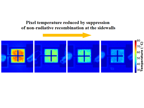 KAIST researchers devises a technology to utilize ultrahigh-resolution micro-LED with 40% reduced self-generated heat
In the digitized modern life, various forms of future displays, such as wearable and rollable displays are required. More and more people are wanting to connect to the virtual world whenever and wherever with the use of their smartglasses or smartwatches. Even further, we’ve been hearing about medical diagnosis kit on a shirt and a theatre-hat. However, it is not quite here in our hands yet due to technical limitations of being unable to fit as many pixels as a limited surface area of a glasses while keeping the power consumption at the a level that a hand held battery can supply, all the while the resolution of 4K+ is needed in order to perfectly immerse the users into the augmented or virtual reality through a wireless smartglasses or whatever the device.
KAIST (President Kwang Hyung Lee) announced on the 22nd that Professor Sang Hyeon Kim's research team of the Department of Electrical and Electronic Engineering re-examined the phenomenon of efficiency degradation of micro-LEDs with pixels in a size of micrometers (μm, one millionth of a meter) and found that it was possible to fundamentally resolve the problem by the use of epitaxial structure engineering.
Epitaxy refers to the process of stacking gallium nitride crystals that are used as a light emitting body on top of an ultrapure silicon or sapphire substrate used for μLEDs as a medium.
μLED is being actively studied because it has the advantages of superior brightness, contrast ratio, and lifespan compared to OLED. In 2018, Samsung Electronics commercialized a product equipped with μLED called 'The Wall'. And there is a prospect that Apple may be launching a μLED-mounted product in 2025.
In order to manufacture μLEDs, pixels are formed by cutting the epitaxial structure grown on a wafer into a cylinder or cuboid shape through an etching process, and this etching process is accompanied by a plasma-based process. However, these plasmas generate defects on the side of the pixel during the pixel formation process.
Therefore, as the pixel size becomes smaller and the resolution increases, the ratio of the surface area to the volume of the pixel increases, and defects on the side of the device that occur during processing further reduce the device efficiency of the μLED. Accordingly, a considerable amount of research has been conducted on mitigating or removing sidewall defects, but this method has a limit to the degree of improvement as it must be done at the post-processing stage after the grown of the epitaxial structure is finished.
The research team identified that there is a difference in the current moving to the sidewall of the μLED depending on the epitaxial structure during μLED device operation, and based on the findings, the team built a structure that is not sensitive to sidewall defects to solve the problem of reduced efficiency due to miniaturization of μLED devices. In addition, the proposed structure reduced the self-generated heat while the device was running by about 40% compared to the existing structure, which is also of great significance in commercialization of ultrahigh-resolution μLED displays.
This study, which was led by Woo Jin Baek of Professor Sang Hyeon Kim's research team at the KAIST School of Electrical and Electronic Engineering as the first author with guidance by Professor Sang Hyeon Kim and Professor Dae-Myeong Geum of the Chungbuk National University (who was with the team as a postdoctoral researcher at the time) as corresponding authors, was published in the international journal, 'Nature Communications' on March 17th. (Title of the paper: Ultra-low-current driven InGaN blue micro light-emitting diodes for electrically efficient and self-heating relaxed microdisplay).
Professor Sang Hyeon Kim said, "This technological development has great meaning in identifying the cause of the drop in efficiency, which was an obstacle to miniaturization of μLED, and solving it with the design of the epitaxial structure.“ He added, ”We are looking forward to it being used in manufacturing of ultrahigh-resolution displays in the future."
This research was carried out with the support of the Samsung Future Technology Incubation Center.
Figure 1. Image of electroluminescence distribution of μLEDs fabricated from epitaxial structures with quantum barriers of different thicknesses while the current is running
Figure 2. Thermal distribution images of devices fabricated with different epitaxial structures under the same amount of light.
Figure 3. Normalized external quantum efficiency of the device fabricated with the optimized epitaxial structure by sizes.
2023.03.23 View 7036
KAIST researchers devises a technology to utilize ultrahigh-resolution micro-LED with 40% reduced self-generated heat
In the digitized modern life, various forms of future displays, such as wearable and rollable displays are required. More and more people are wanting to connect to the virtual world whenever and wherever with the use of their smartglasses or smartwatches. Even further, we’ve been hearing about medical diagnosis kit on a shirt and a theatre-hat. However, it is not quite here in our hands yet due to technical limitations of being unable to fit as many pixels as a limited surface area of a glasses while keeping the power consumption at the a level that a hand held battery can supply, all the while the resolution of 4K+ is needed in order to perfectly immerse the users into the augmented or virtual reality through a wireless smartglasses or whatever the device.
KAIST (President Kwang Hyung Lee) announced on the 22nd that Professor Sang Hyeon Kim's research team of the Department of Electrical and Electronic Engineering re-examined the phenomenon of efficiency degradation of micro-LEDs with pixels in a size of micrometers (μm, one millionth of a meter) and found that it was possible to fundamentally resolve the problem by the use of epitaxial structure engineering.
Epitaxy refers to the process of stacking gallium nitride crystals that are used as a light emitting body on top of an ultrapure silicon or sapphire substrate used for μLEDs as a medium.
μLED is being actively studied because it has the advantages of superior brightness, contrast ratio, and lifespan compared to OLED. In 2018, Samsung Electronics commercialized a product equipped with μLED called 'The Wall'. And there is a prospect that Apple may be launching a μLED-mounted product in 2025.
In order to manufacture μLEDs, pixels are formed by cutting the epitaxial structure grown on a wafer into a cylinder or cuboid shape through an etching process, and this etching process is accompanied by a plasma-based process. However, these plasmas generate defects on the side of the pixel during the pixel formation process.
Therefore, as the pixel size becomes smaller and the resolution increases, the ratio of the surface area to the volume of the pixel increases, and defects on the side of the device that occur during processing further reduce the device efficiency of the μLED. Accordingly, a considerable amount of research has been conducted on mitigating or removing sidewall defects, but this method has a limit to the degree of improvement as it must be done at the post-processing stage after the grown of the epitaxial structure is finished.
The research team identified that there is a difference in the current moving to the sidewall of the μLED depending on the epitaxial structure during μLED device operation, and based on the findings, the team built a structure that is not sensitive to sidewall defects to solve the problem of reduced efficiency due to miniaturization of μLED devices. In addition, the proposed structure reduced the self-generated heat while the device was running by about 40% compared to the existing structure, which is also of great significance in commercialization of ultrahigh-resolution μLED displays.
This study, which was led by Woo Jin Baek of Professor Sang Hyeon Kim's research team at the KAIST School of Electrical and Electronic Engineering as the first author with guidance by Professor Sang Hyeon Kim and Professor Dae-Myeong Geum of the Chungbuk National University (who was with the team as a postdoctoral researcher at the time) as corresponding authors, was published in the international journal, 'Nature Communications' on March 17th. (Title of the paper: Ultra-low-current driven InGaN blue micro light-emitting diodes for electrically efficient and self-heating relaxed microdisplay).
Professor Sang Hyeon Kim said, "This technological development has great meaning in identifying the cause of the drop in efficiency, which was an obstacle to miniaturization of μLED, and solving it with the design of the epitaxial structure.“ He added, ”We are looking forward to it being used in manufacturing of ultrahigh-resolution displays in the future."
This research was carried out with the support of the Samsung Future Technology Incubation Center.
Figure 1. Image of electroluminescence distribution of μLEDs fabricated from epitaxial structures with quantum barriers of different thicknesses while the current is running
Figure 2. Thermal distribution images of devices fabricated with different epitaxial structures under the same amount of light.
Figure 3. Normalized external quantum efficiency of the device fabricated with the optimized epitaxial structure by sizes.
2023.03.23 View 7036 -
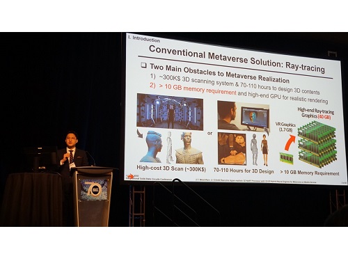 KAIST develops 'MetaVRain' that realizes vivid 3D real-life images
KAIST (President Kwang Hyung Lee) is a high-speed, low-power artificial intelligence (AI: Artificial Intelligent) semiconductor* MetaVRain, which implements artificial intelligence-based 3D rendering that can render images close to real life on mobile devices.
* AI semiconductor: Semiconductor equipped with artificial intelligence processing functions such as recognition, reasoning, learning, and judgment, and implemented with optimized technology based on super intelligence, ultra-low power, and ultra-reliability
The artificial intelligence semiconductor developed by the research team makes the existing ray-tracing*-based 3D rendering driven by GPU into artificial intelligence-based 3D rendering on a newly manufactured AI semiconductor, making it a 3D video capture studio that requires enormous costs. is not needed, so the cost of 3D model production can be greatly reduced and the memory used can be reduced by more than 180 times. In particular, the existing 3D graphic editing and design, which used complex software such as Blender, is replaced with simple artificial intelligence learning, so the general public can easily apply and edit the desired style.
* Ray-tracing: Technology that obtains images close to real life by tracing the trajectory of all light rays that change according to the light source, shape and texture of the object
This research, in which doctoral student Donghyun Han participated as the first author, was presented at the International Solid-State Circuit Design Conference (ISSCC) held in San Francisco, USA from February 18th to 22nd by semiconductor researchers from all over the world.
(Paper Number 2.7, Paper Title: MetaVRain: A 133mW Real-time Hyper-realistic 3D NeRF Processor with 1D-2D Hybrid Neural Engines for Metaverse on Mobile Devices (Authors: Donghyeon Han, Junha Ryu, Sangyeob Kim, Sangjin Kim, and Hoi-Jun Yoo))
Professor Yoo's team discovered inefficient operations that occur when implementing 3D rendering through artificial intelligence, and developed a new concept semiconductor that combines human visual recognition methods to reduce them. When a person remembers an object, he has the cognitive ability to immediately guess what the current object looks like based on the process of starting with a rough outline and gradually specifying its shape, and if it is an object he saw right before. In imitation of such a human cognitive process, the newly developed semiconductor adopts an operation method that grasps the rough shape of an object in advance through low-resolution voxels and minimizes the amount of computation required for current rendering based on the result of rendering in the past.
MetaVRain, developed by Professor Yu's team, achieved the world's best performance by developing a state-of-the-art CMOS chip as well as a hardware architecture that mimics the human visual recognition process. MetaVRain is optimized for artificial intelligence-based 3D rendering technology and achieves a rendering speed of up to 100 FPS or more, which is 911 times faster than conventional GPUs. In addition, as a result of the study, the energy efficiency, which represents the energy consumed per video screen processing, is 26,400 times higher than that of GPU, opening the possibility of artificial intelligence-based real-time rendering in VR/AR headsets and mobile devices.
To show an example of using MetaVRain, the research team developed a smart 3D rendering application system together, and showed an example of changing the style of a 3D model according to the user's preferred style. Since you only need to give artificial intelligence an image of the desired style and perform re-learning, you can easily change the style of the 3D model without the help of complicated software. In addition to the example of the application system implemented by Professor Yu's team, it is expected that various application examples will be possible, such as creating a realistic 3D avatar modeled after a user's face, creating 3D models of various structures, and changing the weather according to the film production environment. do.
Starting with MetaVRain, the research team expects that the field of 3D graphics will also begin to be replaced by artificial intelligence, and revealed that the combination of artificial intelligence and 3D graphics is a great technological innovation for the realization of the metaverse.
Professor Hoi-Jun Yoo of the Department of Electrical and Electronic Engineering at KAIST, who led the research, said, “Currently, 3D graphics are focused on depicting what an object looks like, not how people see it.” The significance of this study was revealed as a study that enabled efficient 3D graphics by borrowing the way people recognize and express objects by imitating them.” He also foresaw the future, saying, “The realization of the metaverse will be achieved through innovation in artificial intelligence technology and innovation in artificial intelligence semiconductors, as shown in this study.”
Figure 1. Description of the MetaVRain demo screen
Photo of Presentation at the International Solid-State Circuits Conference (ISSCC)
2023.03.13 View 7171
KAIST develops 'MetaVRain' that realizes vivid 3D real-life images
KAIST (President Kwang Hyung Lee) is a high-speed, low-power artificial intelligence (AI: Artificial Intelligent) semiconductor* MetaVRain, which implements artificial intelligence-based 3D rendering that can render images close to real life on mobile devices.
* AI semiconductor: Semiconductor equipped with artificial intelligence processing functions such as recognition, reasoning, learning, and judgment, and implemented with optimized technology based on super intelligence, ultra-low power, and ultra-reliability
The artificial intelligence semiconductor developed by the research team makes the existing ray-tracing*-based 3D rendering driven by GPU into artificial intelligence-based 3D rendering on a newly manufactured AI semiconductor, making it a 3D video capture studio that requires enormous costs. is not needed, so the cost of 3D model production can be greatly reduced and the memory used can be reduced by more than 180 times. In particular, the existing 3D graphic editing and design, which used complex software such as Blender, is replaced with simple artificial intelligence learning, so the general public can easily apply and edit the desired style.
* Ray-tracing: Technology that obtains images close to real life by tracing the trajectory of all light rays that change according to the light source, shape and texture of the object
This research, in which doctoral student Donghyun Han participated as the first author, was presented at the International Solid-State Circuit Design Conference (ISSCC) held in San Francisco, USA from February 18th to 22nd by semiconductor researchers from all over the world.
(Paper Number 2.7, Paper Title: MetaVRain: A 133mW Real-time Hyper-realistic 3D NeRF Processor with 1D-2D Hybrid Neural Engines for Metaverse on Mobile Devices (Authors: Donghyeon Han, Junha Ryu, Sangyeob Kim, Sangjin Kim, and Hoi-Jun Yoo))
Professor Yoo's team discovered inefficient operations that occur when implementing 3D rendering through artificial intelligence, and developed a new concept semiconductor that combines human visual recognition methods to reduce them. When a person remembers an object, he has the cognitive ability to immediately guess what the current object looks like based on the process of starting with a rough outline and gradually specifying its shape, and if it is an object he saw right before. In imitation of such a human cognitive process, the newly developed semiconductor adopts an operation method that grasps the rough shape of an object in advance through low-resolution voxels and minimizes the amount of computation required for current rendering based on the result of rendering in the past.
MetaVRain, developed by Professor Yu's team, achieved the world's best performance by developing a state-of-the-art CMOS chip as well as a hardware architecture that mimics the human visual recognition process. MetaVRain is optimized for artificial intelligence-based 3D rendering technology and achieves a rendering speed of up to 100 FPS or more, which is 911 times faster than conventional GPUs. In addition, as a result of the study, the energy efficiency, which represents the energy consumed per video screen processing, is 26,400 times higher than that of GPU, opening the possibility of artificial intelligence-based real-time rendering in VR/AR headsets and mobile devices.
To show an example of using MetaVRain, the research team developed a smart 3D rendering application system together, and showed an example of changing the style of a 3D model according to the user's preferred style. Since you only need to give artificial intelligence an image of the desired style and perform re-learning, you can easily change the style of the 3D model without the help of complicated software. In addition to the example of the application system implemented by Professor Yu's team, it is expected that various application examples will be possible, such as creating a realistic 3D avatar modeled after a user's face, creating 3D models of various structures, and changing the weather according to the film production environment. do.
Starting with MetaVRain, the research team expects that the field of 3D graphics will also begin to be replaced by artificial intelligence, and revealed that the combination of artificial intelligence and 3D graphics is a great technological innovation for the realization of the metaverse.
Professor Hoi-Jun Yoo of the Department of Electrical and Electronic Engineering at KAIST, who led the research, said, “Currently, 3D graphics are focused on depicting what an object looks like, not how people see it.” The significance of this study was revealed as a study that enabled efficient 3D graphics by borrowing the way people recognize and express objects by imitating them.” He also foresaw the future, saying, “The realization of the metaverse will be achieved through innovation in artificial intelligence technology and innovation in artificial intelligence semiconductors, as shown in this study.”
Figure 1. Description of the MetaVRain demo screen
Photo of Presentation at the International Solid-State Circuits Conference (ISSCC)
2023.03.13 View 7171