OT
-
 KAIST Student Wins HRI Student Design Competition
(From left: Jason Jangho Choi, Hyunjin Ku and Wonkyung Do)
Hyunjin Ku from the Department of Mechanical Engineering won the first prize at the Student Design Competition of Human-Robot-Interaction (HRI) 2018 which was held in Chicago.
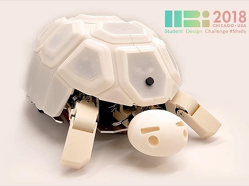
Ku teamed up with undergrad students from Seoul National University (Jason Jangho Choi, Soomin Lee, Sunho Jang, and Wonkyung Do) and submitted Shelly, a tortoise-like robot for one-to-many interactions with children.
Figure 1. Shelly, a tortoise-like robot for one-to-many interactions with children
In the Student Design Competition of the HRI, students from around the globe can submit designs for their interactive robotic objects. The competition focused on human-agent interactions and practical applications.
Ku conducted the research while doing an internship at NAVER Labs. Her research on learning robot abuse with Shelly was published in IEEE Spectrum.
[YTN Science]
https://www.youtube.com/watch?v=n5KVwgBk0wk
[HRI 2018 Website]
http://humanrobotinteraction.org/2018/sdc/
[IEEE Spectrum]
https://spectrum.ieee.org/automaton/robotics/robotics-hardware/shelly-robotic-tortoise-helps-kids-learn-that-robot-abuse-is-a-bad-thing
2018.07.02 View 9322
 -
 Taming AI: Engineering, Ethics, and Policy
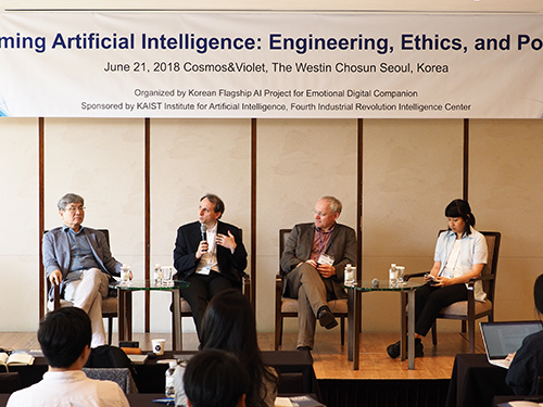
(Professor Lee, Professor Koene, Professor Walsh, and Professor Ema (from left))
Can AI-powered robotics could be adequate companions for humans? Will the good faith of users and developers work for helping AI-powered robots become the new tribe of the digital future?
AI’s efficiency is creating new socio-economic opportunities in the global market. Despite the opportunities, challenges still remain. It is said that efficiency-enforcing algorithms through deep learning will take an eventual toll on human dignity and safety, bringing out the disastrous fiascos featured in the Terminator movies.
A research group at the Korean Flagship AI Project for Emotional Digital Companionship at KAIST Institute for AI (KI4AI) and the Fourth Industrial Intelligence Center at KAIST Institute co-hosted a seminar, “Taming AI: Engineering, Ethics, and Policy” last week to discuss ways to better employ AI technologies in ways that upholds human values.
The KI4AI has been conducting this flagship project from the end of 2016 with the support of the Ministry of Science and ICT.
The seminar brought together three speakers from Australia, Japan, and the UK to better fathom the implications of the new technology emergence from the ethical perspectives of engineering and discuss policymaking for the responsible usage of technology.
Professor Toby Walsh, an anti-autonomous weapon activist from New South Wales University in Australia continued to argue the possible risk that AI poses to malfunction. He said that an independent ethics committee or group usually monitors academic institutions’ research activities in order to avoid any possible mishaps.
However, he said there is no independent group or committee monitoring the nature of corporations’ engagement of such technologies, while its possible threats against humanity are alleged to be growing. He mentioned that Google’s and Amazon’s information collecting also pose a potent threat. He said that ethical standards similar to academic research integrity should be established to avoid the possible restricting of the dignity of humans and mass destruction. He hoped that KAIST and Google would play a leading role in establishing an international norm toward this compelling issue.
Professor Arisa Ema from the University of Tokyo provided very compelling arguments for thinking about the duplicity of technology and how technology should serve the public interest without any bias against gender, race, and social stratum. She pointed out the information dominated by several Western corporations like Google. She said that such algorithms for deep learning of data provided by several Western corporations will create very biased information, only applicable to limited races and classes.
Meanwhile, Professor Ansgar Koene from the University of Nottingham presented the IEEE’s global initiative on the ethics of autonomous and intelligence systems. He shared the cases of industry standards and ethically-aligned designs made by the IEEE Standards Association. He said more than 250 global cross-disciplinary thought leaders from around the world joined to develop ethical guidelines called Ethically Aligned Design (EAD) V2. EAD V2 includes methodologies to guide ethical research and design, embedding values into autonomous intelligence systems among others. For the next step beyond EAD V2, the association is now working for IEEE P70xx Standards Projects, detailing more technical approaches.
Professor Soo Young Lee at KAIST argued that the eventual goal of complete AI is to have human-like emotions, calling it a new paradigm for the relationship between humans and AI-robots. According to Professor Lee, AI-powered robots will serve as a good companion for humans. “Especially in aging societies affecting the globe, this will be a very viable and practical option,” he said.
He pointed out, “Kids learn from parents’ morality and social behavior. Users should have AI-robots learn morality as well. Their relationships should be based on good faith and trust, no longer that of master and slave. He said that liability issues for any mishap will need to be discussed further, but basically each user and developer should have their own responsibility when dealing with these issues.
2018.06.26 View 10052
 -
 KAIST Team Reaching Out with Appropriate Technology
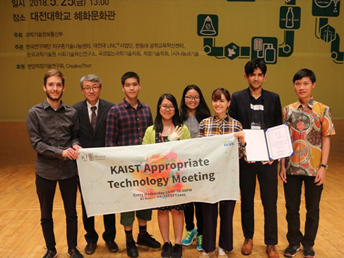
(The gold prize winning team of KATT)
The KAIST Appropriate Technology Team (KATT) consisting of international students at KAIST won the gold and silver prizes at ‘The 10th Creative Design Competition for the Other 90 Percent.’
More than 218 students from 50 teams nationwide participated in the competition hosted by the Ministry of Science and ICT last month.
The competition was created to discover appropriate technology and sustainable design items to enhance the quality of life for those with no or few accessible technologies.
A team led by Juan Luis Gonzalez Bello, graduate student from the School of Electrical Engineering received the gold prize for presenting a prosthetic arm. Their artificial arm was highly recognized for its affordability and good manageability. The team said that it cost less than 10 US dollars to construct from materials available in underprivileged regions and was easy to assemble.
Sophomore Hutomo Calvin from the Department of Materials Science & Engineering also worked on the prosthetic arm project with freshmen Bella Godiva, Stephanie Tan, and Koptieuov Yearbola.
Alexandra Tran, senior from the School of Electrical Engineering led the silver prize winning team. Her team developed a portable weather monitor, ‘Breathe Easy’. She worked with Alisher Tortay, senior from the School of Computing, Ashar Alam, senior from the Department of Mechanical Engineering, Bereket Eshete, junior from the School of Computing, and Marthens Hakzimana, sophomore from the Department of Mechanical Engineering.
This weather monitor is a low-cost but efficient air quality monitor. The team said it just cost less than seven US dollars to construct the monitor.KAIST students have now won the gold prize for two consecutive years.
2018.06.19 View 13196
 -
 Lead-free, Efficient Perovskite for Photovoltaic Cells
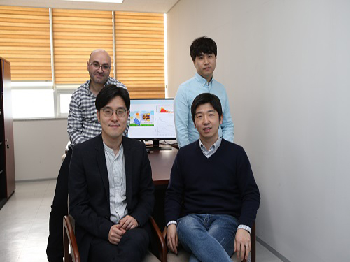
(Clockwise from left: Post-doc Researcher Lamjed Debbichi, Master’s Candidate Songju Lee, Professor Min Seok Jang and Professor Hyungjun Kim)
A KAIST research team has proposed a perovskite material, Cs2Au2I6 that serves as a potential active material for highly efficient lead-free thin-film photovoltaic devices. This material is expected to lay the foundation to overcome previously known limitations of perovskite including its stability and toxicity issues.
As strong candidates for next-generation high-efficiency photovoltaic cells, perovskite photovoltaic cells have a maximum photoconversion efficiency of 22%, comparable to high-performance crystalline silicon photovoltaic cells. In addition, perovskite-based cells can be fabricated at low temperatures, thereby bringing about dramatic cost reductions.
However, it has been noted that conventional organic-inorganic hybrid perovskite materials exhibit low stability, eventually degrading their performance and making them unfit for continued use. Moreover, their inclusion of lead has undermined their environmental friendliness.
In light of this, a joint team led by Professor Hyungjun Kim from the KAIST Department of Chemistry and Professor Min Seok Jang from the School of Electrical Engineering has analyzed a previously discovered perovskite material, Cs2Au2I6, consisting of only inorganic substances and investigated its suitability for application in thin-film photovoltaic devices. Theoretical investigations suggests that this new perovskite material is not only as efficient but also more stable and environment friendly compared to the conventional perovskite materials. For this analysis, the team developed multiscale multiphysics simulation frameworks. Atomic-scale first-principle quantum calculations were carried out to study the optical properties of the proposed material, and device-scale electromagnetic simulations were conducted to suggest that the material could indeed serve as a promising photovoltaic substance at the device level.
From this point onward, the research team plans to extend the study in two directions: an empirical study to apply the perovskite material in real-world photovoltaic cells and a theoretical analysis to find the optimal and highly stable material for photovoltaic cells. The team said, “Perovskite materials are highly efficient, but in order to completely replace the conventional solar cells, their stability and toxicity issues must first be resolved.” They added that this research is expected to accelerate related studies in pursuit of high-efficiency, environment-friendly perovskite materials.
This research, led by post-doc researcher Lamjed Debbichi and master’s candidate Songju Lee, was selected as the front cover article of Advanced Materials on March 22.
Figure 1. Cover of Advanced Materials
Figure 2. Schematic of full solar cell device structure
2018.06.08 View 10087
 -
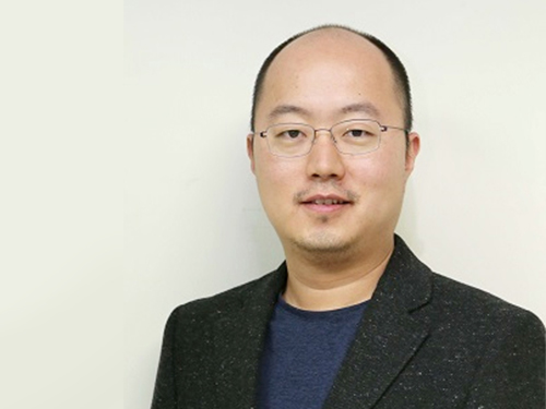 Professor YongKeun Park Wins the 2018 Fumio Okano Award
(Professor Park)
Professor YongKeun Park from the Department of Physics won the 2018 Fumio Okano Award in recognition of his contributions to 3D display technology development during the annual conference of the International Society for Optics and Photonics (SPIE) held last month in Orlando, Florida in the US.
The Fumio Okano Best 3D Paper Prize is presented annually in memory of Dr. Fumio Okano, a pioneer and innovator of 3D displays who passed away in 2013, for his contributions to the field of 3D TVs and displays. The award is sponsored by NHK-ES.
Professor Park and his team are developing novel technology for measuring and visualizing 3D images by applying random light scattering. He has published numerous papers on 3D holographic camera technology and 3000x enhanced performance of 3D holographic displays in renowned international journals such as Nature Photonics, Nature Communications, and Science Advances. His technology has drawn international attention from renowned media outlets including Newsweek and Forbes.
He has established two startups to commercialize his technology. Tomocube specializes in 3D imaging microscopes using holotomographic technology and the company exports their products to several countries including the US and Japan. The.Wave.Talk is exploring technology for examining pre-existing bacteria anywhere and anytime.
Professor Park’s innovations have already been recognized in and out of KAIST. In February, he was selected as the KAISTian of the Year for his outstanding research, commercialization, and startups. He was also decorated with the National Science Award in April by the Ministry of Science and ICT and the Hong Jin-Ki Innovation Award later in May by the Yumin Cultural Foundation.
Professor Park said, “3D holography is emerging as a significant technology with growing potential and positive impacts on our daily lives. However, the current technology lags far behind the levels displayed in SF movies. We will do our utmost to reach this level with more commercialization."
2018.05.31 View 12731
 -
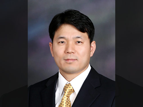 Professor Hee-Sung Park Named Scientist of May
(Professor Hee-Sung Park)
Professor Hee-Sung Park from the Department of Chemistry was named ‘Scientist of May’ sponsored by the Ministry of Science and ICT and the National Research Foundation of Korea. Professor Park was honored in recognition of his developing a tool to engineer designer proteins via diverse chemical modifications. This approach provides a novel platform for investigating numerous diseases such as cancer and dementia.
His research focuses on the production of synthetic proteins and the generation of diverse protein functions as well as the designing and engineering of new translation machinery for genetic code expansion, and the application of synthetic biology techniques for basic cell biology and applied medical science.
Post-translational modifications (PTMs) are constantly taking place during or after protein biosynthesis. PTMs play a vital role in expanding protein functional diversity and, as a result, critically affect numerous biological processes. Abnormal PTMs have been known to trigger various diseases including cancer and dementia. Therefore, this technology enables proteins to reproduce with specific modifications at selected residues and will significantly help establish experimental strategies to investigate fundamental biological mechanisms including the development of targeted cancer therapies.
Professor Park also received 10 million KRW in prize money.
2018.05.04 View 11887
 -
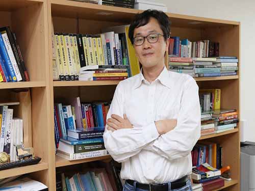 Escalation of Competition Leads to Conflict in Competitive Networks of F1 Drivers
(Professor Wonjae Lee at the Graduate School of Culture Technology)
A new study has revealed that people with similar social status in similar age groups are more likely to clash with each other. This rivalry could likely lead to taking more risks in fair weather conditions.
Competition, while is often seen as beneficial, can escalate into destructive conflict. This occurs, for instance, when athletes sabotage each other or when rival executives get caught up in a career-derailing fight. These escalations, which lead to conflict, are especially likely among similar-status competitors, who are fraught with discordant understandings of who is superior to whom.
A research team of KAIST, the US Treasury, INSEAD, and the European School of Management and Technology (ESMT) examined the link between status similarity and conflict as well as the conditions under which this link holds by using panel data on Formula 1 races from 1970 through 2014. For the study, the research team analyzed a total of 506 collision cases by 355 F1 drivers over 45 years.
The team found that similar-status F1 drivers are more prone to collide, especially when they are age-similar, performing well, and feeling safe. When these boundary conditions are met, structural equivalence likely triggers antagonism among interactants.
This research deepens the understanding of when violent conflict emerges and when prevention efforts are called for. Professor Lee from the Graduate School of Culture Technology at KAIST said, “People are not sure about their identity when facing competitors of a similar status. People tend to confirm their own stature by beating an opponent.”
The team investigated the factors that escalate competition into dangerous conflict. Recently, sociological theorizing claims that such escalations are particularly likely in pairs of structurally equivalent actors who have the same relations with the same third parties. Using the F1 data, the research team modeled the probability that two drivers would collide on a racetrack as a function of their structural equivalence in a dynamic network of competitive relationships.
Professor Lee added, “We fully understand that the drivers who ranked first and second are likely to have more conflict because they meet more frequently and know each other well. We also regulated all those conditions and confirmed that our hypothesis worked right throughout the data analysis.”
Professor Lee, who wrote his doctoral thesis on tennis tournaments for identifying the ideal organizational structure, said that sports tournaments would be best optimized for comprehending the nature of organizational structures. Tournaments, even those with rankings based on objective criteria, are in fact intensely social. However, most prior empirical work in this area has relied only on official information on competitors’ performance, thus failing to capture the important elements of past competitive encounters.
“It is not so easy to obtain data on rivalries and conflicts inside an organization. However, in sports, the performances of athletes are all recorded and the data can be utilized as a very objective methodology for understanding social relations and their structural affects.
Official positions in tournaments, although clearly informative, can also be reductionist –excluding the emotionally salient features of competitors’ histories and forcing competitors together on a scalar metric, even when the competitors themselves do not see each other as comparable.
The results from sample-split models are important for social networking research, which has paid scant attention to the contextual conditions in which structural equivalence is most consequential for social action – especially hostile social actions.
The study suggests that new work will benefit from examining how demographic overlap, network stability, and perceived costs of conflict “activate” a structurally equivalent relationship to the point that it is not only salient but also conducive to conflict.
Professor Lee said, “Sociology mainly investigates the positive results of social success and collaboration. This study shows that any violent activities, including homicide, also have something to do with organizational and social structural equivalence.”
This study was co-led by Professor Matthew Bothner from ESMT in Germany, Professor Henning Piezunk from INSEAD in France, and Dr. Richard Haynes from the US Treasury and was featured at the PNAS (Proceedings of the National Academy of Sciences of the USA) in March.
(Figure: Drivers' competitive network and collisions. Nodes are drivers. Nodes enricled in black are labeled by name. Edges denote joint competition in at least one race. Red edges connecting indicate that the two drivers collided at least once. Using Fruchtermna-Reingold, nodes are generally proximte to the extendt that their average structural equivalence (over all races, from 1970 to 2014) is high.)
2018.04.24 View 7765
 -
 KAIST Develops IoT Platform for Food Safety
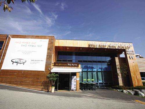
A research team led by the KAIST Auto-ID Labs developed a GS1 international standard-based IoTs infrastructure platform dubbed Oliot (Open Language of Internet of Things). This platform will be applied to Wanju Local Food, the nation’s largest cooperative, and will be in operation from April 5.
A total of eleven organizations participated in the development of Oliot, with KAIST as the center. This consortium is based on the GS1 international standard-based Oliot platform, which allows collecting and sharing data along the entire process of agrifood from production to processing, distribution, and consumption. It aims at increasing farm incomes and establishing a global ecosystem of domestic agriculture and stockbreeding that provides safe food.
Wanju Local Food is now the world’s first local food co-op with a traceability system from the initial stage of production planning to end sales based on GS1 international standards, which will ensure food safety.
KAIST has been sharing Oliot data in order to apply it to industries around the world. As of April 2018, approximately 900 enterprises and developers from more than 100 countries have downloaded it.
Professor Daeyoung Kim from the School of Computing, who is also Research Director of Auto-ID Labs said, “We are planning to disseminate Oliot to local food cooperatives throughout the nation. We will also cooperate with other countries, like China, Holland, and Hong Kong to create a better ecosystem for the global food industry.
“We are currently collaborating with related business to converge Oliot with AI or blockchain technology that can be applied to various services, such as healthcare and smart factories. Its tangible outcome will be revealed soon,” he added.
Auto-ID Labs are a global research consortium of six academic institutions that research and develop new technologies for advancing global commerce, partnering with GS1 (Global Standard 1), a non-profit organization that established standards for global commerce such as introducing barcodes to the retail industry. The Auto-ID Labs include MIT, University of Cambridge, Keio University, Fudan University, ETH Zurich/University of St. Gallen, and KAIST.
The consortium was supported by the Ministry of Science and ICT as well as the Institute for Information and Communications Technology Promotion for three years from 2015.
The launching of Oliot at Wanju Local Food will be held on April 5.
2018.04.03 View 10707
 -
 Seong-Tae Kim Wins Robert-Wagner All-Conference Best Paper Award
(Ph.D. candidate Seong-Tae Kim)
Ph.D. candidate Seong-Tae Kim from the School of Electrical Engineering won the Robert Wagner All-Conference Best Student Paper Award during the 2018 International Society for Optics and Photonics (SPIE) Medical Imaging Conference, which was held in Houston last month.
Kim, supervised by Professor Yong Man Ro, received the award for his paper in the category of computer-aided diagnosis. His paper, titled “ICADx: Interpretable Computer-Aided Diagnosis of Breast Masses”, was selected as the best paper out of 900 submissions. The conference selects the best paper in nine different categories. His research provides new insights on diagnostic technology to detect breast cancer powered by deep learning.
2018.03.15 View 12285
 -
 Professor Jungwon Kim Wins Haerim Optics and Photonics Award
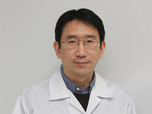
(Professor Jungwon Kim)
Professor Jungwon Kim from the Department of Mechanical Engineering received the 8th Haerim Optics and Photonics Award from the Optical Society of Korea (OSK).
He was recognized for his dedication to pioneering the field of microwave photonics by developing ultra-low noise fiber photonics lasers.
The Haerim Optics and Photonics Award is given to an outstanding researcher who has made academic contributions in the field of optics and photonics for the last five years.
The name of the award (Haerim) comes from the pen-name of the renowned scholar, Professor Un-Chul Paek, because it is maintained using funds he contributed to the OSK.
The OSK will confer the award on February 8 during the 29th OSK Annual Meeting and Winter Conference of 2018.
2018.02.07 View 8994
 -
 KAIST to Host the THE Innovation & Impact Summit in 2019
KAIST and Times Higher Education (THE) agreed to co-host the THE Innovation & Impact Summit at KAIST from April 1 to 3, 2019.
Global leaders from higher education, government, and industry will gather at KAIST to discuss how universities can better innovate for creating a greater impact.
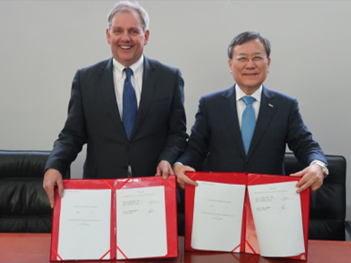
(from left: THE Managing Director Trevor Barratt and KAIST President Sung-Chul Shin)
President Sung-Chul Shin and Trevor Barratt, managing director at the THE, signed an agreement to host the 2019 THE Innovation & Impact Summit at KAIST next April. The agreement was signed on February 6 during the THE Asia Universities Summit held at SUSTech in Shenzhen in China. Phil Baty, editorial director at the THE was also present during the agreement.
By hosting the 2019 THE Innovation & Impact Summit, KAIST has a chance to introduce its innovative research and performance and its educational environment and startup ecosystem to the world. Having educational and industrial leaders meet at KAIST will add more power to the global status and capacity of KAIST.
The THE Innovation & Impact Summit, first held in 2017, is one in the seven presidential summit series held by THE. During the second summit at KAIST, THE will launch their world university innovation rankings for the first time.
As innovation at universities and its impact have been a crucial indicator in building an institutional brand and reputation, leading universities are gearing up to encourage startups and entrepreneurship education. Even more, innovation at universities is emerging as one of the growth engines of economies.
The innovation indicators of KAIST have been highly recognized by many global ranking institutions in terms of the volume of patents and the patents-to-article citation impact. Thomson Reuters has recognized KAIST for two consecutive years as the most innovative university in Asia, and sixth in the world.
President Shin has high expectations for the hosting of the Innovation & Impact Summit at KAIST. He explained, “Innovation makes up the DNA of KAIST and it has been our institutional mission from the start in 1971. KAIST was commissioned to make innovation for industrialization and economic development through education and research. I do not see any university more suitable than KAIST to host this innovation summit. I hope the summit at KAIST will serve as a global platform to provide very creative ideas for making innovation and collaboration among the leading universities for all the participants.”
Meanwhile, at the THE Asia Universities Summit in Shenzhen, how to respond to the implications of the Fourth Industrial Revolution was the key agenda piercing the two-day sessions.
As a panelist, President Shin shared his experiences on innovative strategies viable for spearheading university reform for the Fourth Industrial Revolution, along with Vice-Chancellor of the University of Sheffield Sir Keith Burnett, President of Monash University Margaret Gardner, and President of Hong Kong Polytechnic University President Timothy W. Tong. He said that universities should foster young talents by equipping them with creativity, collaboration, and convergent minds. To swiftly respond to the new industrial environment, President Shin said that universities should remove the high barriers between departments and establish cross- and inter-disciplinary education systems, convergence research and technology commercialization.
2018.02.06 View 10363
 -
 Three Professors Named KAST Fellows
(Professor Dan Keun Sung at the center)
(Professor Y.H. Cho at the center)
(Professor K.H. Cho at the center)
The Korean Academy of Science and Technology (KAST) inducted three KAIST professors as fellows at the New Year’s ceremony held at KAST on January 12. They were among the 24 newly elected fellows of the most distinguished academy in Korea. The new fellows are Professor Dan Keun Sung of the School of Electrical Engineering, Professor Kwang-Hyun Cho of the Department of Bio and Brain Engineering, and Professor Yong-Hoon Cho of the Department of Physics.
Professor Sung was recognized for his lifetime academic achievements in fields related with network protocols and energy ICT. He also played a crucial role in launching the Korean satellites KITSAT-1,2,3 and the establishment of the Satellite Technology Research Center at KAIST.
Professor Y.H.Cho has been a pioneer in the field of low-dimensional semiconductor-powered quantum photonics that enables quantum optical research in solid state. He has been recognized as a renowned scholar in this field internationally.
Professor K.H.Cho has conducted original research that combines IT and BT in systems biology and has applied novel technologies of electronic modeling and computer simulation analysis for investigating complex life sciences. Professor Cho, who is in his 40s, is the youngest fellow among the newly inducted fellows.
2018.01.16 View 16221