Quantum
-
 Realizing Highly Efficient Quantum Dot LEDs with Metallic Nanostructures
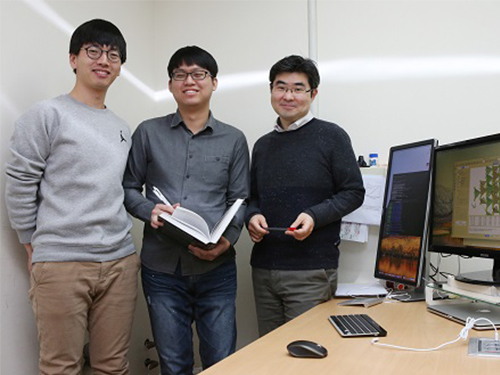
(Professor Yong-Hoon Cho and PhD candidate Hyun Chul Park)
KAIST researchers have discovered a technology that enhances the efficiency of Quantum Dot LEDs.
Professor Yong-Hoon Cho from the Department of Physics and his team succeeded in improving the efficiency of Quantum Dot (QD) Light-Emitting Diodes (LEDs) by designing metallic nanostructure substrates.
QD LEDs possess very small semiconductor light sources and are considered to be the new rising technology for high performance full-color display. However, it is expensive to manufacture displays with QD LED only.
Existing QD-based displays use blue LEDs as a source of light, and they employ a method of color conversion through excitation of green and red QDs.
There are two inconveniences with the existing QD-based displays. As mentioned previously, QD LED is costly, hence the unit price of QD-based displays is higher. Also, the efficiency of a liquid type of QDs is drastically lowered after contact with air.
Professor Cho found the solution in a metallic nanostructure for lowering the production cost while improving the efficiency of QD LEDs.
The team exploited the phenomenon of so-called surface plasmonic resonances when nanoscale metallic structures are exposed to light. Depending on the metal, the size, and the shape, the properties of metallic structures vary.
The team used different metallic nanostructures for each QD LED – silver nanodisks for Red QDs and aluminum nanodisks for Green GDs – to make them more fluorescent.
With brighter QDs, it requires fewer QDs to manufacture QD LEDs, contributing to a lower unit price.
The team used silver and aluminum in this research, but metallic nanostructures can be redesigned according to the desired purposes.
Professor Cho said, “Implementing metallic nanostructures into QD LEDs in a proper manner can reduce the quantity of the QDs required for the system, leading to lower unit prices.”
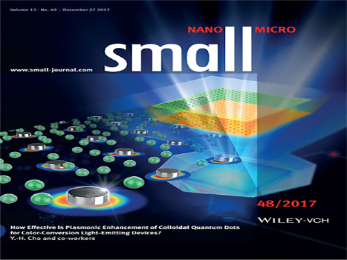
This research, led by PhD candidate Hyun Chul Park, was chosen as the cover of the international journal, Small, on December 27, 2017.
Figure 1. Cover of the journal
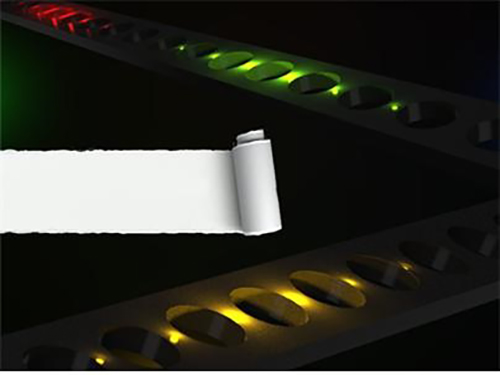
Figure 2. Spectrum showing different fluorescence with and without metallic nanostructure
2018.01.23 View 7217
Realizing Highly Efficient Quantum Dot LEDs with Metallic Nanostructures
(Professor Yong-Hoon Cho and PhD candidate Hyun Chul Park)
KAIST researchers have discovered a technology that enhances the efficiency of Quantum Dot LEDs.
Professor Yong-Hoon Cho from the Department of Physics and his team succeeded in improving the efficiency of Quantum Dot (QD) Light-Emitting Diodes (LEDs) by designing metallic nanostructure substrates.
QD LEDs possess very small semiconductor light sources and are considered to be the new rising technology for high performance full-color display. However, it is expensive to manufacture displays with QD LED only.
Existing QD-based displays use blue LEDs as a source of light, and they employ a method of color conversion through excitation of green and red QDs.
There are two inconveniences with the existing QD-based displays. As mentioned previously, QD LED is costly, hence the unit price of QD-based displays is higher. Also, the efficiency of a liquid type of QDs is drastically lowered after contact with air.
Professor Cho found the solution in a metallic nanostructure for lowering the production cost while improving the efficiency of QD LEDs.
The team exploited the phenomenon of so-called surface plasmonic resonances when nanoscale metallic structures are exposed to light. Depending on the metal, the size, and the shape, the properties of metallic structures vary.
The team used different metallic nanostructures for each QD LED – silver nanodisks for Red QDs and aluminum nanodisks for Green GDs – to make them more fluorescent.
With brighter QDs, it requires fewer QDs to manufacture QD LEDs, contributing to a lower unit price.
The team used silver and aluminum in this research, but metallic nanostructures can be redesigned according to the desired purposes.
Professor Cho said, “Implementing metallic nanostructures into QD LEDs in a proper manner can reduce the quantity of the QDs required for the system, leading to lower unit prices.”
This research, led by PhD candidate Hyun Chul Park, was chosen as the cover of the international journal, Small, on December 27, 2017.
Figure 1. Cover of the journal
Figure 2. Spectrum showing different fluorescence with and without metallic nanostructure
2018.01.23 View 7217 -
 New Quantum Mechanical States Observed
(Professor Han (far right) and his research team)
A KAIST research team observed a new quantum mechanical magnetic state ‘Jeff = 3/2.’ This first observation of ‘Jeff=3/2’ could be the foundation for future research on superconductivity and quantum magnetism.
In quantum mechanics, total angular momentum is defined as the sum of spin and orbital angular momenta and is denoted with the ‘J.’ The newly identified magnetic moment can be described as a kind of angular momentum that occurs when specific conditions are met and has been denoted ‘Jeff’ with the meaning ‘effective angular momentum’ in the field. Jeff=3/2 has been a topic of discussion but was yet to be observed.
The research was co-led by Professor Myung Joon Han of the Department of Physics at Chung-Ang University in Korea, RIKEN in Japan, and the Argonne National Laboratory in the US. This research was published in Nature Communications on October 14, 2017.
In academia, spin-orbital coupling was known to lead to a unique quantum state and has been an active area of recent research. In contrast to magnetic moment by electron spin and orbital, the effective magnetic moment Jeff, formed from the coupling of the two, shows a unique ground state and interaction patterns, which could lead to new phenomena and properties.
Most studies in the last decade focused on ‘Jeff=1/2’, but there has not been any observation of ‘Jeff=3/2’, which led to slow progress. In 2014, the research team led by Prof. Han theoretically predicted the possibility of the ‘Jeff=3/2’ state in a certain type of materials based on molecular orbital, instead of atomic orbital. In the current study, the team applied the Selection Rule of quantum mechanics for the ‘Jeff=3/2’ state, which differs to the general spin moment, in order to experimentally detect this moment.
When electrons near the atomic nucleus are excited by X-rays, the excited electrons can be absorbed or re-emitted through interactions with other electrons. Here, the Selection Rule is applied to electrons. According to quantum mechanics, this rule is very unique in the ‘Jeff=3/2’ state and ‘Jeff=3/2’ is predicted to be distinguishable from general spin states. The prediction that was made using this idea was verified through the experiment using electrons extracted from tantalum at two different energy levels. In this material, the unique quantum mechanical interference by the ‘Jeff=3/2’ moment can be taken as direct evidence for its existence.
The new quantum state is very unique from any of the previously known magnetic states and this study could be the starting point for future research on the ‘Jeff=3/2’ moment. Further, this finding could contribute to future research on various properties of the magnetic states and its interactions.
(Figure 1: Crystal structure, MO levels, and RIXS process in GaTa4Se8.)
(Figure 2: Cluster model calculations of the L3 and L2 RIXS spectra)
2017.12.14 View 5948
New Quantum Mechanical States Observed
(Professor Han (far right) and his research team)
A KAIST research team observed a new quantum mechanical magnetic state ‘Jeff = 3/2.’ This first observation of ‘Jeff=3/2’ could be the foundation for future research on superconductivity and quantum magnetism.
In quantum mechanics, total angular momentum is defined as the sum of spin and orbital angular momenta and is denoted with the ‘J.’ The newly identified magnetic moment can be described as a kind of angular momentum that occurs when specific conditions are met and has been denoted ‘Jeff’ with the meaning ‘effective angular momentum’ in the field. Jeff=3/2 has been a topic of discussion but was yet to be observed.
The research was co-led by Professor Myung Joon Han of the Department of Physics at Chung-Ang University in Korea, RIKEN in Japan, and the Argonne National Laboratory in the US. This research was published in Nature Communications on October 14, 2017.
In academia, spin-orbital coupling was known to lead to a unique quantum state and has been an active area of recent research. In contrast to magnetic moment by electron spin and orbital, the effective magnetic moment Jeff, formed from the coupling of the two, shows a unique ground state and interaction patterns, which could lead to new phenomena and properties.
Most studies in the last decade focused on ‘Jeff=1/2’, but there has not been any observation of ‘Jeff=3/2’, which led to slow progress. In 2014, the research team led by Prof. Han theoretically predicted the possibility of the ‘Jeff=3/2’ state in a certain type of materials based on molecular orbital, instead of atomic orbital. In the current study, the team applied the Selection Rule of quantum mechanics for the ‘Jeff=3/2’ state, which differs to the general spin moment, in order to experimentally detect this moment.
When electrons near the atomic nucleus are excited by X-rays, the excited electrons can be absorbed or re-emitted through interactions with other electrons. Here, the Selection Rule is applied to electrons. According to quantum mechanics, this rule is very unique in the ‘Jeff=3/2’ state and ‘Jeff=3/2’ is predicted to be distinguishable from general spin states. The prediction that was made using this idea was verified through the experiment using electrons extracted from tantalum at two different energy levels. In this material, the unique quantum mechanical interference by the ‘Jeff=3/2’ moment can be taken as direct evidence for its existence.
The new quantum state is very unique from any of the previously known magnetic states and this study could be the starting point for future research on the ‘Jeff=3/2’ moment. Further, this finding could contribute to future research on various properties of the magnetic states and its interactions.
(Figure 1: Crystal structure, MO levels, and RIXS process in GaTa4Se8.)
(Figure 2: Cluster model calculations of the L3 and L2 RIXS spectra)
2017.12.14 View 5948 -
 Semiconductor Photonic Nanocavities on Paper Substrates
Professor Yong-Hoon Cho of the Department of Physics and his team at KAIST have developed a semiconductor photonic nanocavity laser that can operate on a paper substrate.
The researchers hope that this novel method, which involves transferring nano-sized photonic crystal particles onto a paper substrate with high absorptiveness, will enable the diagnoses of various diseases by using high-tech semiconductor sensors at low cost.
The results of this research were published in the November 17th, 2016, issue of Advanced Materials.
Photonic crystals, which utilize light as a medium to provide high bandwidths, can transfer large amounts of information. Compared with their electronic counterparts, photonic crystals also consume less energy to operate.
Normally, semiconductor photonic particles require substrates, which play only a passive role in the assembly and endurance of individual, functional photonic components. These substrates, however, are bulky and environmentally hazardous as they are made up of non-biodegradable materials.
The research team overcame these two shortcomings by replacing a semiconductor substrate with standard paper. The substrate’s mass was reduced considerably, and because paper is made from trees, it degrades. Paper can be easily and cheaply acquired from our surroundings, which drastically reduces the unit cost of semiconductors.
In addition, paper possesses superior mechanical characteristics. It is flexible and can be repeatedly folded and unfolded without being torn. These are traits that have long been sought by researchers for existing flexible substrates.
The research team used a micro-sized stamp to detach photonic crystal nanobeam cavities selectively from their original substrate and transfer them onto a new paper substrate. Using this technique, the team removed nanophotonic crystals that had been patterned (using a process of selectively etching circuits onto a substrate) onto a semiconductor substrate with a high degree of integration, and realigned them as desired on a paper substrate.
The nanophotonic crystals that the team combined with paper in this research were 0.5 micrometers in width, 6 micrometers in length, and 0.3 micrometers in height—about one-hundredth of the width of a single hair (0.1 millimeter).
The team also transferred their photonic crystals onto paper with a fluid channel, which proved that it could be used as a refractive index sensor. As can be seen in current commercial pregnancy diagnosis kits, paper has high absorptiveness. Since photonic crystal particles have high sensitivity, they are highly suitable for applications such as sensors.
Professor Cho stated that “by using paper substrates, this technology can greatly contribute to the rising field of producing environmentally-friendly photonic particles” and “by combining inexpensive paper and high-performance photonic crystal sensors, we can obtain low prices as well as designing appropriate technologies with high performance.”
Dr. Sejeong Kim of the Department of Physics participated in this study as the first author, and Professor Kwanwoo Shin of Sogang University and Professor Yong-Hee Lee of KAIST also took part in this research. The research was supported by the National Research Foundation’s Mid-Career Researcher Program, and the Climate Change Research Hub of KAIST.
Figure 1. Illustration of photonic crystal lasers on paper substrates
Figure 2. Photonic crystal resonator laser and refractive index sensor operating on paper substrates
2017.03.01 View 7710
Semiconductor Photonic Nanocavities on Paper Substrates
Professor Yong-Hoon Cho of the Department of Physics and his team at KAIST have developed a semiconductor photonic nanocavity laser that can operate on a paper substrate.
The researchers hope that this novel method, which involves transferring nano-sized photonic crystal particles onto a paper substrate with high absorptiveness, will enable the diagnoses of various diseases by using high-tech semiconductor sensors at low cost.
The results of this research were published in the November 17th, 2016, issue of Advanced Materials.
Photonic crystals, which utilize light as a medium to provide high bandwidths, can transfer large amounts of information. Compared with their electronic counterparts, photonic crystals also consume less energy to operate.
Normally, semiconductor photonic particles require substrates, which play only a passive role in the assembly and endurance of individual, functional photonic components. These substrates, however, are bulky and environmentally hazardous as they are made up of non-biodegradable materials.
The research team overcame these two shortcomings by replacing a semiconductor substrate with standard paper. The substrate’s mass was reduced considerably, and because paper is made from trees, it degrades. Paper can be easily and cheaply acquired from our surroundings, which drastically reduces the unit cost of semiconductors.
In addition, paper possesses superior mechanical characteristics. It is flexible and can be repeatedly folded and unfolded without being torn. These are traits that have long been sought by researchers for existing flexible substrates.
The research team used a micro-sized stamp to detach photonic crystal nanobeam cavities selectively from their original substrate and transfer them onto a new paper substrate. Using this technique, the team removed nanophotonic crystals that had been patterned (using a process of selectively etching circuits onto a substrate) onto a semiconductor substrate with a high degree of integration, and realigned them as desired on a paper substrate.
The nanophotonic crystals that the team combined with paper in this research were 0.5 micrometers in width, 6 micrometers in length, and 0.3 micrometers in height—about one-hundredth of the width of a single hair (0.1 millimeter).
The team also transferred their photonic crystals onto paper with a fluid channel, which proved that it could be used as a refractive index sensor. As can be seen in current commercial pregnancy diagnosis kits, paper has high absorptiveness. Since photonic crystal particles have high sensitivity, they are highly suitable for applications such as sensors.
Professor Cho stated that “by using paper substrates, this technology can greatly contribute to the rising field of producing environmentally-friendly photonic particles” and “by combining inexpensive paper and high-performance photonic crystal sensors, we can obtain low prices as well as designing appropriate technologies with high performance.”
Dr. Sejeong Kim of the Department of Physics participated in this study as the first author, and Professor Kwanwoo Shin of Sogang University and Professor Yong-Hee Lee of KAIST also took part in this research. The research was supported by the National Research Foundation’s Mid-Career Researcher Program, and the Climate Change Research Hub of KAIST.
Figure 1. Illustration of photonic crystal lasers on paper substrates
Figure 2. Photonic crystal resonator laser and refractive index sensor operating on paper substrates
2017.03.01 View 7710 -
 Development of a Photonic Diode with Light Speed, Single-Direction Transfer
A photonic diode using a nitride semiconductor rod can increase the possibility of developing all-optical integrated circuits, an alternative to conventional integrated circuits.
Professor Yong-Hoon Cho's research team from the Department of Physics, KAIST, developed a photonic diode which can selectively transfer light in one way, using semiconductor rods.
The photonic diode has a diameter of hundreds of nanometers (nm) and a length of few micrometers. This size enables its use in large-scale integration (LSI). The diode’s less sensitivity towards polarized light angle makes it more useful.
In an integrated circuit, a diode controls the flow of electrons. If this diode controls light rather than electrons, data can be transferred at high speed, and its loss is minimized to a greater extent. Since these implementations conserve more energy, this is a very promising future technology.
However, conventional electronic diodes, made up of asymmetric meta-materials or photonic crystalline structures, are large, which makes them difficult to be used in LSI. These diodes could only be implemented under limited conditions due to its sensitivity towards polarized light angle.
The research team used nitride semiconductor rods to develop a highly efficient photonic diode with distinct light intensities from opposite ends.
The semiconductor rod yields different amount of energy horizontally. According to the research team, this is because the width of the quantum well and its indium quantity is continuously controlled.
Professor Cho said, "A large energy difference in a horizontal direction causes asymmetrical light propagation, enabling it to be operated as a photonic diode." He added that “If light, instead of electrons, were adopted in integrated circuits, the transfer speed would be expected as great as that of light.”
The research findings were published in the September 10th issue of Nano Letters as the cover paper.
Under the guidance of Professor Cho, two Ph.D. candidates, Suk-Min Ko and Su-Hyun Gong, conducted this research. This research project was sponsored by the National Research Foundation of Korea and KAIST’s EEWS (energy, environment, water, and sustainability) Research Center.
Figure Description: Computer simulated image of photonic diode made of semiconductor rod implemented in an all-optical integrated circuit
2014.09.23 View 11758
Development of a Photonic Diode with Light Speed, Single-Direction Transfer
A photonic diode using a nitride semiconductor rod can increase the possibility of developing all-optical integrated circuits, an alternative to conventional integrated circuits.
Professor Yong-Hoon Cho's research team from the Department of Physics, KAIST, developed a photonic diode which can selectively transfer light in one way, using semiconductor rods.
The photonic diode has a diameter of hundreds of nanometers (nm) and a length of few micrometers. This size enables its use in large-scale integration (LSI). The diode’s less sensitivity towards polarized light angle makes it more useful.
In an integrated circuit, a diode controls the flow of electrons. If this diode controls light rather than electrons, data can be transferred at high speed, and its loss is minimized to a greater extent. Since these implementations conserve more energy, this is a very promising future technology.
However, conventional electronic diodes, made up of asymmetric meta-materials or photonic crystalline structures, are large, which makes them difficult to be used in LSI. These diodes could only be implemented under limited conditions due to its sensitivity towards polarized light angle.
The research team used nitride semiconductor rods to develop a highly efficient photonic diode with distinct light intensities from opposite ends.
The semiconductor rod yields different amount of energy horizontally. According to the research team, this is because the width of the quantum well and its indium quantity is continuously controlled.
Professor Cho said, "A large energy difference in a horizontal direction causes asymmetrical light propagation, enabling it to be operated as a photonic diode." He added that “If light, instead of electrons, were adopted in integrated circuits, the transfer speed would be expected as great as that of light.”
The research findings were published in the September 10th issue of Nano Letters as the cover paper.
Under the guidance of Professor Cho, two Ph.D. candidates, Suk-Min Ko and Su-Hyun Gong, conducted this research. This research project was sponsored by the National Research Foundation of Korea and KAIST’s EEWS (energy, environment, water, and sustainability) Research Center.
Figure Description: Computer simulated image of photonic diode made of semiconductor rod implemented in an all-optical integrated circuit
2014.09.23 View 11758 -
 An Electron Cloud Distribution Observed by the Scanning Seebeck Microscope
All matters are made of small particles, namely atoms. An atom is composed of a heavy nucleus and cloud-like, extremely light electrons.
Korean researchers developed an electron microscopy technique that enables the accurate observation of an electron cloud distribution at room-temperature. The achievement is comparable to the invention of the quantum tunneling microscopy technique developed 33 years ago.
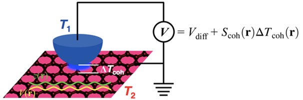
Professor Yong-Hyun Kim of the Graduate School of Nanoscience and Technology at KAIST and Dr. Ho-Gi Yeo of the Korea Research Institute of Standards and Science (KRISS) developed the Scanning Seebeck Microscope (SSM). The SSM renders clear images of atoms, as well as an electron cloud distribution. This was achieved by creating a voltage difference via a temperature gradient.
The development was introduced in the online edition of Physical Review Letters (April 2014), a prestigious journal published by the American Institute of Physics.
The SSM is expected to be economically competitive as it gives high resolution images at an atomic scale even for graphene and semiconductors, both at room temperature. In addition, if the SSM is applied to thermoelectric material research, it will contribute to the development of high-efficiency thermoelectric materials.
Through numerous hypotheses and experiments, scientists now believe that there exists an electron cloud surrounding a nucleus. IBM's Scanning Tunneling Microscope (STM) was the first to observe the electron cloud and has remained as the only technique to this day. The developers of IBM microscope, Dr. Gerd Binnig and Dr. Heinrich Rohrer, were awarded the 1986 Nobel Prize in Physics.
There still remains a downside to the STM technique, however: it required high precision and extreme low temperature and vibration. The application of voltage also affects the electron cloud, resulting in a distorted image.
The KAIST research team adopted a different approach by using the Seebeck effect which refers to the voltage generation due to a temperature gradient between two materials.
The team placed an observation sample (graphene) at room temperature (37~57℃) and detected its voltage generation. This technique made it possible to observe an electron cloud at room temperature.
Furthermore, the research team investigated the theoretical quantum mechanics behind the electron cloud using the observation gained through the Seebeck effect and also obtained by simulation capability to analyze the experimental results.
The research was a joint research project between KAIST Professor Yong-Hyun Kim and KRISS researcher Dr. Ho-Gi Yeo. Eui-Seop Lee, a Ph.D. candidate of KAIST, and KRISS researcher Dr. Sang-Hui Cho also participated. The Ministry of Science, ICT, and Future Planning, the Global Frontier Initiative, and the Disruptive Convergent Technology Development Initiative funded the project in Korea.
Picture 1: Schematic Diagram of the Scanning Seebeck Microscope (SSM)
Picture 2: Electron cloud distribution observed by SSM at room temperature
Picture 3: Professor Yong-Hyun Kim
2014.04.04 View 15159
An Electron Cloud Distribution Observed by the Scanning Seebeck Microscope
All matters are made of small particles, namely atoms. An atom is composed of a heavy nucleus and cloud-like, extremely light electrons.
Korean researchers developed an electron microscopy technique that enables the accurate observation of an electron cloud distribution at room-temperature. The achievement is comparable to the invention of the quantum tunneling microscopy technique developed 33 years ago.
Professor Yong-Hyun Kim of the Graduate School of Nanoscience and Technology at KAIST and Dr. Ho-Gi Yeo of the Korea Research Institute of Standards and Science (KRISS) developed the Scanning Seebeck Microscope (SSM). The SSM renders clear images of atoms, as well as an electron cloud distribution. This was achieved by creating a voltage difference via a temperature gradient.
The development was introduced in the online edition of Physical Review Letters (April 2014), a prestigious journal published by the American Institute of Physics.
The SSM is expected to be economically competitive as it gives high resolution images at an atomic scale even for graphene and semiconductors, both at room temperature. In addition, if the SSM is applied to thermoelectric material research, it will contribute to the development of high-efficiency thermoelectric materials.
Through numerous hypotheses and experiments, scientists now believe that there exists an electron cloud surrounding a nucleus. IBM's Scanning Tunneling Microscope (STM) was the first to observe the electron cloud and has remained as the only technique to this day. The developers of IBM microscope, Dr. Gerd Binnig and Dr. Heinrich Rohrer, were awarded the 1986 Nobel Prize in Physics.
There still remains a downside to the STM technique, however: it required high precision and extreme low temperature and vibration. The application of voltage also affects the electron cloud, resulting in a distorted image.
The KAIST research team adopted a different approach by using the Seebeck effect which refers to the voltage generation due to a temperature gradient between two materials.
The team placed an observation sample (graphene) at room temperature (37~57℃) and detected its voltage generation. This technique made it possible to observe an electron cloud at room temperature.
Furthermore, the research team investigated the theoretical quantum mechanics behind the electron cloud using the observation gained through the Seebeck effect and also obtained by simulation capability to analyze the experimental results.
The research was a joint research project between KAIST Professor Yong-Hyun Kim and KRISS researcher Dr. Ho-Gi Yeo. Eui-Seop Lee, a Ph.D. candidate of KAIST, and KRISS researcher Dr. Sang-Hui Cho also participated. The Ministry of Science, ICT, and Future Planning, the Global Frontier Initiative, and the Disruptive Convergent Technology Development Initiative funded the project in Korea.
Picture 1: Schematic Diagram of the Scanning Seebeck Microscope (SSM)
Picture 2: Electron cloud distribution observed by SSM at room temperature
Picture 3: Professor Yong-Hyun Kim
2014.04.04 View 15159 -
 Short Wavelength, Ultra-High Speed Quantum Light Source based on Quantum Dot Developed
Professor Yong Hoon, Cho (Department of Physics) and his research team synthesized an obelisk nanostructure and successfully formed a single semiconductor quantum exhibiting high reliability to realize an ultra-high speed, highly efficient, release of quantum dots.
The result of the research effort was published in the July 5th online edition of Scientific Reports published by Nature.
Semiconductor Quantum Dots restrict electrons within a cubic boundary of few nanometers thereby exhibiting similar properties to an atom with discontinuous energy levels. Exploitation of this characteristic makes possible the development of quantum light source, critical for next generation quantum information communication and quantum encryption.
High operational temperatures, stability, rapid photon release, electric current capability, and other advantages are reasons why semiconductor quantum dots are regarded as next generation core technology.
However conventional, spontaneously formed quantum dots are densely packed in a planar structure rendering the analysis of a single quantum dot difficult and result in the poor efficiency of photon release. In addition, the internal electromagnetic effect which is caused by inter-planar stress results in low internal quantum efficiency due to the difficulty in electron-hole recombination.
Professor Cho’s research team synthesized an obelisk shaped nanostructure using nitrides that emit short wavelengths of light. The activation layer was grown on the tip of the nanostructure and the team succeeded in placing a single quantum dot on the nano-tip. The team was therefore able to confirm the ultra-high speed single photon characteristics which occur at low energy levels.
Use of unique nanostructures makes synthesis of single atomic structures without processes like patterning while enabling the release of light emitted by the quantum dot.
Using this unique method the team showed the increase in internal quantum efficiency. The electromagnetic forces apparent in thin films no longer affects the quantum dot greatly due to the obelisk structure’s reduced inter planar stress.
The newly developed quantum light source emits visible light (400nm range) and not the conventional infrared light. This characteristic makes possible it use in communication in free space and enables use of highly efficient, visible range photon detector.
Professor Cho commented that “the developed method makes quantum dot growth much easier making single photon synthesis much faster to contribute to the development of practical quantum light source.” And that “the characteristics of the obelisk nanostructure enable the easy detachment from and attachment to other substrates enabling its use in producing single chip quantum light source.”
The research was conducted under the supervision of Professor Cho. The researchers werey Jae Hyung, Kim (first author) and Yong Ho, Ko (second author), both Ph.D. candidates at KAIST. The Ministry of Science, ICT and Future Planning, the National Research Foundation, and WCU Program provided support to the research effort.
2013.08.23 View 8836
Short Wavelength, Ultra-High Speed Quantum Light Source based on Quantum Dot Developed
Professor Yong Hoon, Cho (Department of Physics) and his research team synthesized an obelisk nanostructure and successfully formed a single semiconductor quantum exhibiting high reliability to realize an ultra-high speed, highly efficient, release of quantum dots.
The result of the research effort was published in the July 5th online edition of Scientific Reports published by Nature.
Semiconductor Quantum Dots restrict electrons within a cubic boundary of few nanometers thereby exhibiting similar properties to an atom with discontinuous energy levels. Exploitation of this characteristic makes possible the development of quantum light source, critical for next generation quantum information communication and quantum encryption.
High operational temperatures, stability, rapid photon release, electric current capability, and other advantages are reasons why semiconductor quantum dots are regarded as next generation core technology.
However conventional, spontaneously formed quantum dots are densely packed in a planar structure rendering the analysis of a single quantum dot difficult and result in the poor efficiency of photon release. In addition, the internal electromagnetic effect which is caused by inter-planar stress results in low internal quantum efficiency due to the difficulty in electron-hole recombination.
Professor Cho’s research team synthesized an obelisk shaped nanostructure using nitrides that emit short wavelengths of light. The activation layer was grown on the tip of the nanostructure and the team succeeded in placing a single quantum dot on the nano-tip. The team was therefore able to confirm the ultra-high speed single photon characteristics which occur at low energy levels.
Use of unique nanostructures makes synthesis of single atomic structures without processes like patterning while enabling the release of light emitted by the quantum dot.
Using this unique method the team showed the increase in internal quantum efficiency. The electromagnetic forces apparent in thin films no longer affects the quantum dot greatly due to the obelisk structure’s reduced inter planar stress.
The newly developed quantum light source emits visible light (400nm range) and not the conventional infrared light. This characteristic makes possible it use in communication in free space and enables use of highly efficient, visible range photon detector.
Professor Cho commented that “the developed method makes quantum dot growth much easier making single photon synthesis much faster to contribute to the development of practical quantum light source.” And that “the characteristics of the obelisk nanostructure enable the easy detachment from and attachment to other substrates enabling its use in producing single chip quantum light source.”
The research was conducted under the supervision of Professor Cho. The researchers werey Jae Hyung, Kim (first author) and Yong Ho, Ko (second author), both Ph.D. candidates at KAIST. The Ministry of Science, ICT and Future Planning, the National Research Foundation, and WCU Program provided support to the research effort.
2013.08.23 View 8836 -
New LEDs: Large Spectrum of Colors
Professor Yonghun Cho has discovered that LEDs with hexagonal pyramid structures can emit various colors of light.
LEDs, which have been leading the light revolution is a light emitting element that uses the characteristics of semiconductors to emit light upon passing a current, and is being used for lighting, TV, and various signaling devices.
In general, the white LED used for lighting has to be constructed by spraying yellow fluorescent material on a blue LED or by creating a complicated circuit where various LED chips function together.
Prof.Cho’s research team discovered the fact that when a small hexagonal pyramid structure is formed on the semiconductor composing the LED and a current is passed through this, then each side, edge, and point on the pyramid assumes different energies.
Due to the energy differences, lights of bluegreen, yellow, and orange were emitted from the side, edge, and points of the pyramid, respectively. This shows the prospect of displaying white light as well as that of many other colors.
Thus, applying the nanopyramidal structure to LEDs will allow the emission of light with a large spectrum with just the flow of the current, enabling a new type of LED light emitting particles that would display various colors from a single LED chip without the use of a fluorescent material.
Also, originally, LEDs have had limitations to its efficiency because of its structural characteristics where fluorescent materials had to be sprayed on, but the nanopyramidal structures will overcome this structural barrier to create brighter light
2012.01.31 View 8027