Semiconductors
-
 Controlling Crystal Size of Organic Semiconductors
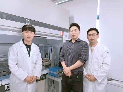
A KAIST research team led by Professor Steve Park from the Department of Materials Science and Engineering
Recently, solution-processable organic semiconductors are being highlighted for their potential application in printed electronics, becoming a feasible technique to fabricate large-area flexible thin film at a low cost. The field-effect mobility of small-molecule organic semiconductors is dependent on the crystallinity, crystal orientation, and crystal size. A variety of solution-based coating techniques, such as ink-jet printing, dip-coating, and solution shearing have been developed to control the crystallinity and crystal orientation, but a method for developing techniques to increase the crystal size of organic semiconductors is still needed.
To overcome this issue, the research team developed an inorganic polymer micropillar-based solution shearing system to increase the crystal size of an organic semiconductor with pillar size. Using this technique, the crystallization process of organic semiconductors can be controlled precisely, and therefore large-area organic semiconductor thin film with controlled crystallinity can be fabricated.
A variety of solution-based coating techniques cannot control the fluid-flow of solutions appropriately, so the solvent evaporates randomly onto the substrate, which has difficulty in the fabrication of organic semiconductor thin film with a large crystal size.
The research team integrated inorganic polymer microstructures into the solution shearing blade to solve this issue. The inorganic polymer can easily be microstructured via conventional molding techniques, has high mechanical durability, and organic solvent resistance. Using the inorganic polymer-based microstructure blade, the research team controlled the size of small molecule organic semiconductors by tuning the shape and dimensions of the microstructure. The microstructures in the blade induce the sharp curvature regions in the meniscus line that formed between the shearing blade and the substrate, and therefore nucleation and crystal growth can be regulated. Hence, the research team fabricated organic semiconductor thin-film with large crystals, which increases the field-effect mobility.
The research team also demonstrated a solution shearing process on a curved surface by using a flexible inorganic polymer-based shearing blade, which expands the applicability of solution shearing.
Professor Park said, “Our new solution shearing system can control the crystallization process precisely during solvent evaporation.” He added, “This technique adds another key parameter that can be utilized to tune the property of thin films and opens up a wide variety of new applications.
The results of this work entitled “Inorganic Polymer Micropillar-Based Solution Shearing of Large-Area Organic Semiconductor Thin Films with Pillar-Size-Dependent Crystal Size” was published in the July 2018 issue of Advanced Materials as a cover article.
2018.10.30 View 6352
 -
 Levitating 2D Semiconductor for Better Performance
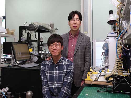
(from top: Professor Yeon Sik Jung and PhD candidate Soomin Yim)
Atomically thin 2D semiconductors have been drawing attention for their superior physical properties over silicon semiconductors; nevertheless, they are not the most appealing materials due to their structural instability and costly manufacturing process. To shed some light on these limitations, a KAIST research team suspended a 2D semiconductor on a dome-shaped nanostructure to produce a highly efficient semiconductor at a low cost.
2D semiconducting materials have emerged as alternatives for silicon-based semiconductors because of their inherent flexibility, high transparency, and excellent carrier transport properties, which are the important characteristics for flexible electronics.
Despite their outstanding physical and chemical properties, they are oversensitive to their environment due to their extremely thin nature. Hence, any irregularities in the supporting surface can affect the properties of 2D semiconductors and make it more difficult to produce reliable and well performing devices. In particular, it can result in serious degradation of charge-carrier mobility or light-emission yield.
To solve this problem, there have been continued efforts to fundamentally block the substrate effects. One way is to suspend a 2D semiconductor; however, this method will degrade mechanical durability due to the absence of a supporter underneath the 2D semiconducting materials.
Professor Yeon Sik Jung from the Department of Materials Science and Engineering and his team came up with a new strategy based on the insertion of high-density topographic patterns as a nanogap-containing supporter between 2D materials and the substrate in order to mitigate their contact and to block the substrate-induced unwanted effects.
More than 90% of the dome-shaped supporter is simply an empty space because of its nanometer scale size. Placing a 2D semiconductor on this structure creates a similar effect to levitating the layer. Hence, this method secures the mechanical durability of the device while minimizing the undesired effects from the substrate. By applying this method to the 2D semiconductor, the charge-carrier mobility was more than doubled, showing a significant improvement of the performance of the 2D semiconductor.
Additionally, the team reduced the price of manufacturing the semiconductor. In general, constructing an ultra-fine dome structure on a surface generally involves costly equipment to create individual patterns on the surface. However, the team employed a method of self-assembling nanopatterns in which molecules assemble themselves to form a nanostructure. This method led to reducing production costs and showed good compatibility with conventional semiconductor manufacturing processes.
Professor Jung said, “This research can be applied to improve devices using various 2D semiconducting materials as well as devices using graphene, a metallic 2D material. It will be useful in a broad range of applications, such as the material for the high speed transistor channels for next-generation flexible displays or for the active layer in light detectors.”
This research, led by PhD candidate Soomin Yim, was published in Nano Letters in April.
Figure 1. Image of a 2D semiconductor using dome structures
2018.08.28 View 6891
 -
 The 2014 Wearable Computer Competition Takes Place at KAIST
“This is a smart wig for patients who are reluctant to go outdoors because their hair is falling out from cancer treatment.”
A graduate student from Sungkyunkwan University, Jee-Hoon Lee enthusiastically explains his project at the KAIST KI Building where the 2014 Wearable Computer Competition was held. He said, “The sensor embedded inside the wig monitors the heart rate and the body temperature, and during an emergency, the device warns the patient about the situation. The product emphasizes two aspects; it notifies the patient in emergency situations, and it encourages patients to perform outdoor activities by enhancing their looks.”
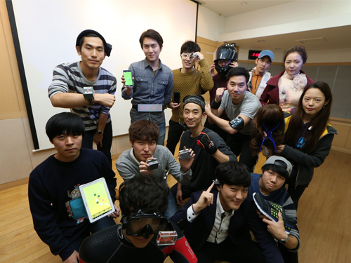
The the tenth anniversary meeting of the 2014 Wearable Computer Competition took place at the KAIST campus on November 13-14, 2014.
A wearable computer is a mobile device designed to be put on the body or clothes so that a user can comfortably use it while walking. Recently, these devices that are able to support versatile internet-based services through smartphones are receiving a great deal of attention.
Wearable devices have been employed in two categorizes: health checks and information-entertainment. In this year’s competition, six healthcare products and nine information-entertainment products were exhibited.
Among these products, participants favored a smart helmet for motorcycle drivers. The driver can see through a rear camera with a navigation screen of the smartphone and text messages through the screen installed in the front glass of the helmet. Another product included a uniform that can control presentation slides by means of motion detection and voice recognition technology. Yet another popular device offered an insole to guide travelers to their destination with the help of motion sensors.
The chairman of the competition, Professor Hoi-Jun Yoo from the Department of Electrical Engineering at KAIST said, “Wearable devices such as smart watches, glasses, and clothes are gaining interest these days. Through this event, people will have a chance to look at the creativity of our students through the display of their wearable devices. In turn, these devices will advance computer technology.”
The third annual wearable computer workshop on convergence technology of wearable computers followed the competition. In the workshop, experts from leading information technology companies such as Samsung Electronics, LG Electronics, and KT Corporation addressed the convergence technology of wearable computers and trends in the field.
2014.11.19 View 11028