Nano
-
 Military Combatants Usher in an Era of Personalized Training with New Materials
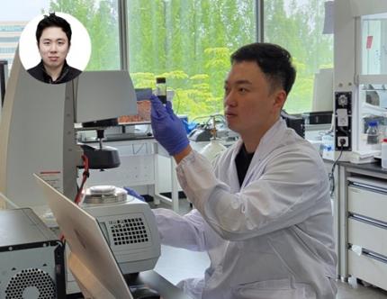
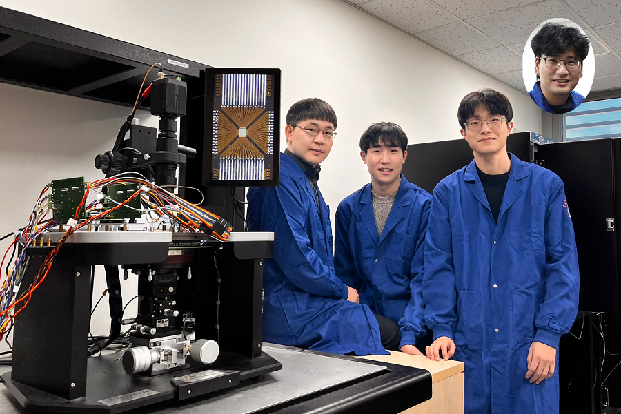
< Photo 1. (From left) Professor Steve Park of Materials Science and Engineering, Kyusoon Pak, Ph.D. Candidate (Army Major) >
Traditional military training often relies on standardized methods, which has limited the provision of optimized training tailored to individual combatants' characteristics or specific combat situations. To address this, our research team developed an e-textile platform, securing core technology that can reflect the unique traits of individual combatants and various combat scenarios. This technology has proven robust enough for battlefield use and is economical enough for widespread distribution to a large number of troops.
On June 25th, Professor Steve Park's research team at KAIST's Department of Materials Science and Engineering announced the development of a flexible, wearable electronic textile (E-textile) platform using an innovative technology that 'draws' electronic circuits directly onto fabric.
The wearable e-textile platform developed by the research team combines 3D printing technology with new materials engineering design to directly print flexible and highly durable sensors and electrodes onto textile substrates. This enables the collection of precise movement and human body data from individual combatants, which can then be used to propose customized training models.
Existing e-textile fabrication methods were often complex or limited in their ability to provide personalized customization. To overcome these challenges, the research team adopted an additive manufacturing technology called 'Direct Ink Writing (DIW)' 3D printing.
< Figure 1. Schematic diagram of e-textile manufactured with Direct Ink Writing (DIW) printing technology on various textiles, including combat uniforms >
This technology involves directly dispensing and printing special ink, which functions as sensors and electrodes, onto textile substrates in desired patterns. This allows for flexible implementation of various designs without the complex process of mask fabrication. This is expected to be an effective technology that can be easily supplied to hundreds of thousands of military personnel.
The core of this technology lies in the development of high-performance functional inks based on advanced materials engineering design. The research team combined styrene-butadiene-styrene (SBS) polymer, which provides flexibility, with multi-walled carbon nanotubes (MWCNT) for electrical conductivity. They developed a tensile/bending sensor ink that can stretch up to 102% and maintain stable performance even after 10,000 repetitive tests. This means that accurate data can be consistently obtained even during the strenuous movements of combatants.
< Figure 2. Measurement of human movement and breathing patterns using e-textile >
Furthermore, new material technology was applied to implement 'interconnect electrodes' that electrically connect the upper and lower layers of the fabric. The team developed an electrode ink combining silver (Ag) flakes with rigid polystyrene (PS) polymer, precisely controlling the impregnation level (how much the ink penetrates the fabric) to effectively connect both sides or multiple layers of the fabric. This secures the technology for producing multi-layered wearable electronic systems integrating sensors and electrodes.
< Figure 3. Experimental results of recognizing unknown objects after machine learning six objects using a smart glove >
The research team proved the platform's performance through actual human movement monitoring experiments. They printed the developed e-textile on major joint areas of clothing (shoulders, elbows, knees) and measured movements and posture changes during various exercises such as running, jumping jacks, and push-ups in real-time.
Additionally, they demonstrated the potential for applications such as monitoring breathing patterns using a smart mask and recognizing objects through machine learning and perceiving complex tactile information by printing multiple sensors and electrodes on gloves. These results show that the developed e-textile platform is effective in precisely understanding the movement dynamics of combatants.
This research is an important example demonstrating how cutting-edge new material technology can contribute to the advancement of the defense sector. Major Kyusoon Pak of the Army, who participated in this research, considered required objectives such as military applicability and economic feasibility for practical distribution from the research design stage.
< Figure 4. Experimental results showing that a multi-layered e-textile glove connected with interconnect electrodes can measure tensile/bending signals and pressure signals at a single point >
Major Pak stated, "Our military is currently facing both a crisis and an opportunity due to the decrease in military personnel resources caused by the demographic cliff and the advancement of science and technology. Also, respect for life in the battlefield is emerging as a significant issue. This research aims to secure original technology that can provide customized training according to military branch/duty and type of combat, thereby enhancing the combat power and ensuring the survivability of our soldiers."
He added, "I hope this research will be evaluated as a case that achieved both scientific contribution and military applicability."
This research, where Kyusoon Pak, Ph.D. Candidate (Army Major) from KAIST's Department of Materials Science and Engineering, participated as the first author and Professor Steve Park supervised, was published on May 27, 2025, in `npj Flexible Electronics (top 1.8% in JCR field)', an international academic journal in the electrical, electronic, and materials engineering fields.
* Paper Title: Fabrication of Multifunctional Wearable Interconnect E-textile Platform Using Direct Ink Writing (DIW) 3D Printing
* DOI: https://doi.org/10.1038/s41528-025-00414-7
This research was supported by the Ministry of Trade, Industry and Energy and the National Research Foundation of Korea.
2025.06.25 View 207
Military Combatants Usher in an Era of Personalized Training with New Materials
< Photo 1. (From left) Professor Steve Park of Materials Science and Engineering, Kyusoon Pak, Ph.D. Candidate (Army Major) >
Traditional military training often relies on standardized methods, which has limited the provision of optimized training tailored to individual combatants' characteristics or specific combat situations. To address this, our research team developed an e-textile platform, securing core technology that can reflect the unique traits of individual combatants and various combat scenarios. This technology has proven robust enough for battlefield use and is economical enough for widespread distribution to a large number of troops.
On June 25th, Professor Steve Park's research team at KAIST's Department of Materials Science and Engineering announced the development of a flexible, wearable electronic textile (E-textile) platform using an innovative technology that 'draws' electronic circuits directly onto fabric.
The wearable e-textile platform developed by the research team combines 3D printing technology with new materials engineering design to directly print flexible and highly durable sensors and electrodes onto textile substrates. This enables the collection of precise movement and human body data from individual combatants, which can then be used to propose customized training models.
Existing e-textile fabrication methods were often complex or limited in their ability to provide personalized customization. To overcome these challenges, the research team adopted an additive manufacturing technology called 'Direct Ink Writing (DIW)' 3D printing.
< Figure 1. Schematic diagram of e-textile manufactured with Direct Ink Writing (DIW) printing technology on various textiles, including combat uniforms >
This technology involves directly dispensing and printing special ink, which functions as sensors and electrodes, onto textile substrates in desired patterns. This allows for flexible implementation of various designs without the complex process of mask fabrication. This is expected to be an effective technology that can be easily supplied to hundreds of thousands of military personnel.
The core of this technology lies in the development of high-performance functional inks based on advanced materials engineering design. The research team combined styrene-butadiene-styrene (SBS) polymer, which provides flexibility, with multi-walled carbon nanotubes (MWCNT) for electrical conductivity. They developed a tensile/bending sensor ink that can stretch up to 102% and maintain stable performance even after 10,000 repetitive tests. This means that accurate data can be consistently obtained even during the strenuous movements of combatants.
< Figure 2. Measurement of human movement and breathing patterns using e-textile >
Furthermore, new material technology was applied to implement 'interconnect electrodes' that electrically connect the upper and lower layers of the fabric. The team developed an electrode ink combining silver (Ag) flakes with rigid polystyrene (PS) polymer, precisely controlling the impregnation level (how much the ink penetrates the fabric) to effectively connect both sides or multiple layers of the fabric. This secures the technology for producing multi-layered wearable electronic systems integrating sensors and electrodes.
< Figure 3. Experimental results of recognizing unknown objects after machine learning six objects using a smart glove >
The research team proved the platform's performance through actual human movement monitoring experiments. They printed the developed e-textile on major joint areas of clothing (shoulders, elbows, knees) and measured movements and posture changes during various exercises such as running, jumping jacks, and push-ups in real-time.
Additionally, they demonstrated the potential for applications such as monitoring breathing patterns using a smart mask and recognizing objects through machine learning and perceiving complex tactile information by printing multiple sensors and electrodes on gloves. These results show that the developed e-textile platform is effective in precisely understanding the movement dynamics of combatants.
This research is an important example demonstrating how cutting-edge new material technology can contribute to the advancement of the defense sector. Major Kyusoon Pak of the Army, who participated in this research, considered required objectives such as military applicability and economic feasibility for practical distribution from the research design stage.
< Figure 4. Experimental results showing that a multi-layered e-textile glove connected with interconnect electrodes can measure tensile/bending signals and pressure signals at a single point >
Major Pak stated, "Our military is currently facing both a crisis and an opportunity due to the decrease in military personnel resources caused by the demographic cliff and the advancement of science and technology. Also, respect for life in the battlefield is emerging as a significant issue. This research aims to secure original technology that can provide customized training according to military branch/duty and type of combat, thereby enhancing the combat power and ensuring the survivability of our soldiers."
He added, "I hope this research will be evaluated as a case that achieved both scientific contribution and military applicability."
This research, where Kyusoon Pak, Ph.D. Candidate (Army Major) from KAIST's Department of Materials Science and Engineering, participated as the first author and Professor Steve Park supervised, was published on May 27, 2025, in `npj Flexible Electronics (top 1.8% in JCR field)', an international academic journal in the electrical, electronic, and materials engineering fields.
* Paper Title: Fabrication of Multifunctional Wearable Interconnect E-textile Platform Using Direct Ink Writing (DIW) 3D Printing
* DOI: https://doi.org/10.1038/s41528-025-00414-7
This research was supported by the Ministry of Trade, Industry and Energy and the National Research Foundation of Korea.
2025.06.25 View 207 -
 KAIST's Li-Fi - Achieves 100 Times Faster Speed and Enhanced Security of Wi-Fi
- KAIST-KRISS Develop 'On-Device Encryption Optical Transmitter' Based on Eco-Friendly Quantum Dots
- New Li-Fi Platform Technology Achieves High Performance with 17.4% Device Efficiency and 29,000 nit Brightness, Simultaneously Improving Transmission Speed and Security
- Presents New Methodology for High-Speed and Encrypted Communication Through Single-Device-Based Dual-Channel Optical Modulation
< Photo 1. (Front row from left) Seungmin Shin, First Author; Professor Himchan Cho; (Back row from left) Hyungdoh Lee, Seungwoo Lee, Wonbeom Lee; (Top left) Dr. Kyung-geun Lim >
Li-Fi (Light Fidelity) is a wireless communication technology that utilizes the visible light spectrum (400-800 THz), similar to LED light, offering speeds up to 100 times faster than existing Wi-Fi (up to 224 Gbps). While it has fewer limitations in available frequency allocation and less radio interference, it is relatively vulnerable to security breaches as anyone can access it. Korean researchers have now proposed a new Li-Fi platform that overcomes the limitations of conventional optical communication devices and can simultaneously enhance both transmission speed and security.
KAIST (President Kwang Hyung Lee) announced on the 24th that Professor Himchan Cho's research team from the Department of Materials Science and Engineering, in collaboration with Dr. Kyung-geun Lim of the Korea Research Institute of Standards and Science (KRISS, President Ho-Seong Lee) under the National Research Council of Science & Technology (NST, Chairman Young-Sik Kim), has developed 'on-device encryption optical communication device' technology for the utilization of 'Li-Fi,' which is attracting attention as a next-generation ultra-high-speed data communication.
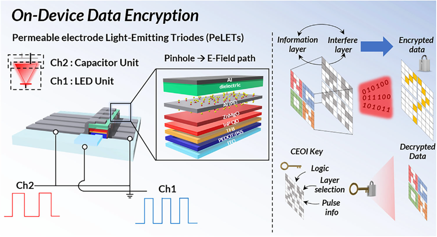
Professor Cho's team created high-efficiency light-emitting triode devices using eco-friendly quantum dots (low-toxicity and sustainable materials). The device developed by the research team is a mechanism that generates light using an electric field. Specifically, the electric field is concentrated in 'tiny holes (pinholes) in the permeable electrode' and transmitted beyond the electrode. This device utilizes this principle to simultaneously process two input data streams.
Using this principle, the research team developed a technology called 'on-device encryption optical transmitter.' The core of this technology is that the device itself converts information into light and simultaneously encrypts it. This means that enhanced security data transmission is possible without the need for complex, separate equipment.
External Quantum Efficiency (EQE) is an indicator of how efficiently electricity is converted into light, with a general commercialization standard of about 20%. The newly developed device recorded an EQE of 17.4%, and its luminance was 29,000 nit, significantly exceeding the maximum brightness of a smartphone OLED screen, which is 2,000 nit, demonstrating a brightness more than 10 times higher.
< Figure 1. Schematic diagram of the device structure developed by the research team and encrypted communication >
Furthermore, to more accurately understand how this device converts information into light, the research team used a method called 'transient electroluminescence analysis.' They analyzed the light-emitting characteristics generated by the device when voltage was instantaneously applied for very short durations (hundreds of nanoseconds = billionths of a second). Through this analysis, they investigated the movement of charges within the device at hundreds of nanoseconds, elucidating the operating mechanism of dual-channel optical modulation implemented within a single device.
Professor Himchan Cho of KAIST stated, "This research overcomes the limitations of existing optical communication devices and proposes a new communication platform that can both increase transmission speed and enhance security."
< Photo 2. Professor Himchan Cho, Department of Materials Science and Engineering >
He added, "This technology, which strengthens security without additional equipment and simultaneously enables encryption and transmission, can be widely applied in various fields where security is crucial in the future."
This research, with Seungmin Shin, a Ph.D. candidate at KAIST's Department of Materials Science and Engineering, participating as the first author, and Professor Himchan Cho and Dr. Kyung-geun Lim of KRISS as co-corresponding authors, was published in the international journal 'Advanced Materials' on May 30th and was selected as an inside front cover paper.※ Paper Title: High-Efficiency Quantum Dot Permeable electrode Light-Emitting Triodes for Visible-Light Communications and On-Device Data Encryption※ DOI: https://doi.org/10.1002/adma.202503189
This research was supported by the National Research Foundation of Korea, the National Research Council of Science & Technology (NST), and the Korea Institute for Advancement of Technology.
2025.06.24 View 646
KAIST's Li-Fi - Achieves 100 Times Faster Speed and Enhanced Security of Wi-Fi
- KAIST-KRISS Develop 'On-Device Encryption Optical Transmitter' Based on Eco-Friendly Quantum Dots
- New Li-Fi Platform Technology Achieves High Performance with 17.4% Device Efficiency and 29,000 nit Brightness, Simultaneously Improving Transmission Speed and Security
- Presents New Methodology for High-Speed and Encrypted Communication Through Single-Device-Based Dual-Channel Optical Modulation
< Photo 1. (Front row from left) Seungmin Shin, First Author; Professor Himchan Cho; (Back row from left) Hyungdoh Lee, Seungwoo Lee, Wonbeom Lee; (Top left) Dr. Kyung-geun Lim >
Li-Fi (Light Fidelity) is a wireless communication technology that utilizes the visible light spectrum (400-800 THz), similar to LED light, offering speeds up to 100 times faster than existing Wi-Fi (up to 224 Gbps). While it has fewer limitations in available frequency allocation and less radio interference, it is relatively vulnerable to security breaches as anyone can access it. Korean researchers have now proposed a new Li-Fi platform that overcomes the limitations of conventional optical communication devices and can simultaneously enhance both transmission speed and security.
KAIST (President Kwang Hyung Lee) announced on the 24th that Professor Himchan Cho's research team from the Department of Materials Science and Engineering, in collaboration with Dr. Kyung-geun Lim of the Korea Research Institute of Standards and Science (KRISS, President Ho-Seong Lee) under the National Research Council of Science & Technology (NST, Chairman Young-Sik Kim), has developed 'on-device encryption optical communication device' technology for the utilization of 'Li-Fi,' which is attracting attention as a next-generation ultra-high-speed data communication.
Professor Cho's team created high-efficiency light-emitting triode devices using eco-friendly quantum dots (low-toxicity and sustainable materials). The device developed by the research team is a mechanism that generates light using an electric field. Specifically, the electric field is concentrated in 'tiny holes (pinholes) in the permeable electrode' and transmitted beyond the electrode. This device utilizes this principle to simultaneously process two input data streams.
Using this principle, the research team developed a technology called 'on-device encryption optical transmitter.' The core of this technology is that the device itself converts information into light and simultaneously encrypts it. This means that enhanced security data transmission is possible without the need for complex, separate equipment.
External Quantum Efficiency (EQE) is an indicator of how efficiently electricity is converted into light, with a general commercialization standard of about 20%. The newly developed device recorded an EQE of 17.4%, and its luminance was 29,000 nit, significantly exceeding the maximum brightness of a smartphone OLED screen, which is 2,000 nit, demonstrating a brightness more than 10 times higher.
< Figure 1. Schematic diagram of the device structure developed by the research team and encrypted communication >
Furthermore, to more accurately understand how this device converts information into light, the research team used a method called 'transient electroluminescence analysis.' They analyzed the light-emitting characteristics generated by the device when voltage was instantaneously applied for very short durations (hundreds of nanoseconds = billionths of a second). Through this analysis, they investigated the movement of charges within the device at hundreds of nanoseconds, elucidating the operating mechanism of dual-channel optical modulation implemented within a single device.
Professor Himchan Cho of KAIST stated, "This research overcomes the limitations of existing optical communication devices and proposes a new communication platform that can both increase transmission speed and enhance security."
< Photo 2. Professor Himchan Cho, Department of Materials Science and Engineering >
He added, "This technology, which strengthens security without additional equipment and simultaneously enables encryption and transmission, can be widely applied in various fields where security is crucial in the future."
This research, with Seungmin Shin, a Ph.D. candidate at KAIST's Department of Materials Science and Engineering, participating as the first author, and Professor Himchan Cho and Dr. Kyung-geun Lim of KRISS as co-corresponding authors, was published in the international journal 'Advanced Materials' on May 30th and was selected as an inside front cover paper.※ Paper Title: High-Efficiency Quantum Dot Permeable electrode Light-Emitting Triodes for Visible-Light Communications and On-Device Data Encryption※ DOI: https://doi.org/10.1002/adma.202503189
This research was supported by the National Research Foundation of Korea, the National Research Council of Science & Technology (NST), and the Korea Institute for Advancement of Technology.
2025.06.24 View 646 -
 KAIST-UIUC researchers develop a treatment platform to disable the ‘biofilm’ shield of superbugs
< (From left) Ph.D. Candidate Joo Hun Lee (co-author), Professor Hyunjoon Kong (co-corresponding author) and Postdoctoral Researcher Yujin Ahn (co-first author) from the Department of Chemical and Biomolecular Engineering of the University of Illinois at Urbana-Champaign and Ju Yeon Chung (co-first author) from the Integrated Master's and Doctoral Program, and Professor Hyun Jung Chung (co-corresponding author) from the Department of Biological Sciences of KAIST >
A major cause of hospital-acquired infections, the super bacteria Methicillin-resistant Staphylococcus aureus (MRSA), not only exhibits strong resistance to existing antibiotics but also forms a dense biofilm that blocks the effects of external treatments. To meet this challenge, KAIST researchers, in collaboration with an international team, successfully developed a platform that utilizes microbubbles to deliver gene-targeted nanoparticles capable of break ing down the biofilms, offering an innovative solution for treating infections resistant to conventional antibiotics.
KAIST (represented by President Kwang Hyung Lee) announced on May 29 that a research team led by Professor Hyun Jung Chung from the Department of Biological Sciences, in collaboration with Professor Hyunjoon Kong's team at the University of Illinois, has developed a microbubble-based nano-gene delivery platform (BTN MB) that precisely delivers gene suppressors into bacteria to effectively remove biofilms formed by MRSA.
The research team first designed short DNA oligonucleotides that simultaneously suppress three major MRSA genes, related to—biofilm formation (icaA), cell division (ftsZ), and antibiotic resistance (mecA)—and engineered nanoparticles (BTN) to effectively deliver them into the bacteria.
< Figure 1. Effective biofilm treatment using biofilm-targeting nanoparticles controlled by microbubbler system. Schematic illustration of BTN delivery with microbubbles (MB), enabling effective permeation of ASOs targeting bacterial genes within biofilms infecting skin wounds. Gene silencing of targets involved in biofilm formation, bacterial proliferation, and antibiotic resistance leads to effective biofilm removal and antibacterial efficacy in vivo. >
In addition, microbubbles (MB) were used to increase the permeability of the microbial membrane, specifically the biofilm formed by MRSA. By combining these two technologies, the team implemented a dual-strike strategy that fundamentally blocks bacterial growth and prevents resistance acquisition.
This treatment system operates in two stages. First, the MBs induce pressure changes within the bacterial biofilm, allowing the BTNs to penetrate. Then, the BTNs slip through the gaps in the biofilm and enter the bacteria, delivering the gene suppressors precisely. This leads to gene regulation within MRSA, simultaneously blocking biofilm regeneration, cell proliferation, and antibiotic resistance expression.
In experiments conducted in a porcine skin model and a mouse wound model infected with MRSA biofilm, the BTN MB treatment group showed a significant reduction in biofilm thickness, as well as remarkable decreases in bacterial count and inflammatory responses.
< Figure 2. (a) Schematic illustration on the evaluation of treatment efficacy of BTN-MB gene therapy. (b) Reduction in MRSA biofilm mass via simultaneous inhibition of multiple genes. (c, d) Antibacterial efficacy of BTN-MB over time in a porcine skin infection biofilm model. (e) Schematic of the experimental setup to verify antibacterial efficacy in a mouse skin wound infection model. (f) Wound healing effects in mice. (g) Antibacterial effects at the wound site. (h) Histological analysis results. >
These results are difficult to achieve with conventional antibiotic monotherapy and demonstrate the potential for treating a wide range of resistant bacterial infections.
Professor Hyun Jung Chung of KAIST, who led the research, stated, “This study presents a new therapeutic solution that combines nanotechnology, gene suppression, and physical delivery strategies to address superbug infections that existing antibiotics cannot resolve. We will continue our research with the aim of expanding its application to systemic infections and various other infectious diseases.”
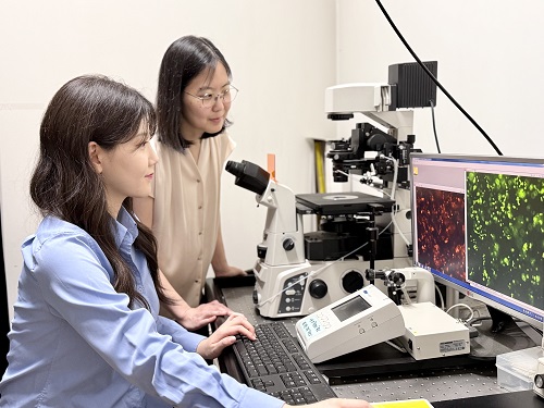
< (From left) Ju Yeon Chung from the Integrated Master's and Doctoral Program, and Professor Hyun Jung Chung from the Department of Biological Sciences >
The study was co-first authored by Ju Yeon Chung, a graduate student in the Department of Biological Sciences at KAIST, and Dr. Yujin Ahn from the University of Illinois. The study was published online on May 19 in the journal, Advanced Functional Materials.
※ Paper Title: Microbubble-Controlled Delivery of Biofilm-Targeting Nanoparticles to Treat MRSA Infection ※ DOI: https://doi.org/10.1002/adfm.202508291
This study was supported by the National Research Foundation and the Ministry of Health and Welfare, Republic of Korea; and the National Science Foundation and National Institutes of Health, USA.
2025.05.29 View 1639
KAIST-UIUC researchers develop a treatment platform to disable the ‘biofilm’ shield of superbugs
< (From left) Ph.D. Candidate Joo Hun Lee (co-author), Professor Hyunjoon Kong (co-corresponding author) and Postdoctoral Researcher Yujin Ahn (co-first author) from the Department of Chemical and Biomolecular Engineering of the University of Illinois at Urbana-Champaign and Ju Yeon Chung (co-first author) from the Integrated Master's and Doctoral Program, and Professor Hyun Jung Chung (co-corresponding author) from the Department of Biological Sciences of KAIST >
A major cause of hospital-acquired infections, the super bacteria Methicillin-resistant Staphylococcus aureus (MRSA), not only exhibits strong resistance to existing antibiotics but also forms a dense biofilm that blocks the effects of external treatments. To meet this challenge, KAIST researchers, in collaboration with an international team, successfully developed a platform that utilizes microbubbles to deliver gene-targeted nanoparticles capable of break ing down the biofilms, offering an innovative solution for treating infections resistant to conventional antibiotics.
KAIST (represented by President Kwang Hyung Lee) announced on May 29 that a research team led by Professor Hyun Jung Chung from the Department of Biological Sciences, in collaboration with Professor Hyunjoon Kong's team at the University of Illinois, has developed a microbubble-based nano-gene delivery platform (BTN MB) that precisely delivers gene suppressors into bacteria to effectively remove biofilms formed by MRSA.
The research team first designed short DNA oligonucleotides that simultaneously suppress three major MRSA genes, related to—biofilm formation (icaA), cell division (ftsZ), and antibiotic resistance (mecA)—and engineered nanoparticles (BTN) to effectively deliver them into the bacteria.
< Figure 1. Effective biofilm treatment using biofilm-targeting nanoparticles controlled by microbubbler system. Schematic illustration of BTN delivery with microbubbles (MB), enabling effective permeation of ASOs targeting bacterial genes within biofilms infecting skin wounds. Gene silencing of targets involved in biofilm formation, bacterial proliferation, and antibiotic resistance leads to effective biofilm removal and antibacterial efficacy in vivo. >
In addition, microbubbles (MB) were used to increase the permeability of the microbial membrane, specifically the biofilm formed by MRSA. By combining these two technologies, the team implemented a dual-strike strategy that fundamentally blocks bacterial growth and prevents resistance acquisition.
This treatment system operates in two stages. First, the MBs induce pressure changes within the bacterial biofilm, allowing the BTNs to penetrate. Then, the BTNs slip through the gaps in the biofilm and enter the bacteria, delivering the gene suppressors precisely. This leads to gene regulation within MRSA, simultaneously blocking biofilm regeneration, cell proliferation, and antibiotic resistance expression.
In experiments conducted in a porcine skin model and a mouse wound model infected with MRSA biofilm, the BTN MB treatment group showed a significant reduction in biofilm thickness, as well as remarkable decreases in bacterial count and inflammatory responses.
< Figure 2. (a) Schematic illustration on the evaluation of treatment efficacy of BTN-MB gene therapy. (b) Reduction in MRSA biofilm mass via simultaneous inhibition of multiple genes. (c, d) Antibacterial efficacy of BTN-MB over time in a porcine skin infection biofilm model. (e) Schematic of the experimental setup to verify antibacterial efficacy in a mouse skin wound infection model. (f) Wound healing effects in mice. (g) Antibacterial effects at the wound site. (h) Histological analysis results. >
These results are difficult to achieve with conventional antibiotic monotherapy and demonstrate the potential for treating a wide range of resistant bacterial infections.
Professor Hyun Jung Chung of KAIST, who led the research, stated, “This study presents a new therapeutic solution that combines nanotechnology, gene suppression, and physical delivery strategies to address superbug infections that existing antibiotics cannot resolve. We will continue our research with the aim of expanding its application to systemic infections and various other infectious diseases.”
< (From left) Ju Yeon Chung from the Integrated Master's and Doctoral Program, and Professor Hyun Jung Chung from the Department of Biological Sciences >
The study was co-first authored by Ju Yeon Chung, a graduate student in the Department of Biological Sciences at KAIST, and Dr. Yujin Ahn from the University of Illinois. The study was published online on May 19 in the journal, Advanced Functional Materials.
※ Paper Title: Microbubble-Controlled Delivery of Biofilm-Targeting Nanoparticles to Treat MRSA Infection ※ DOI: https://doi.org/10.1002/adfm.202508291
This study was supported by the National Research Foundation and the Ministry of Health and Welfare, Republic of Korea; and the National Science Foundation and National Institutes of Health, USA.
2025.05.29 View 1639 -
 No More Touch Issues on Rainy Days! KAIST Develops Human-Like Tactile Sensor
Recent advancements in robotics have enabled machines to handle delicate objects like eggs with precision, thanks to highly integrated pressure sensors that provide detailed tactile feedback. However, even the most advanced robots struggle to accurately detect pressure in complex environments involving water, bending, or electromagnetic interference. A research team at KAIST has successfully developed a pressure sensor that operates stably without external interference, even on wet surfaces like a smartphone screen covered in water, achieving human-level tactile sensitivity.
KAIST (represented by President Kwang Hyung Lee) announced on the 10th of March that a research team led by Professor Jun-Bo Yoon from the School of Electrical Engineering has developed a high-resolution pressure sensor that remains unaffected by external interference such as "ghost touches" caused by moisture on touchscreens.
Capacitive pressure sensors, widely used in touch systems due to their simple structure and durability, are essential components of human-machine interface (HMI) technologies in smartphones, wearable devices, and robots. However, they are prone to malfunctions caused by water droplets, electromagnetic interference, and curves.
To address these issues, the research team investigated the root causes of interference in capacitive pressure sensors. They identified that the "fringe field" generated at the sensor’s edges is particularly susceptible to external disturbances.
The researchers concluded that, to fundamentally resolve this issue, suppressing the fringe field was necessary. Through theoretical analysis, they determined that reducing the electrode spacing to the nanometer scale could effectively minimize the fringe field to below a few percent.
Utilizing proprietary micro/nanofabrication techniques, the team developed a nanogap pressure sensor with an electrode spacing of 900 nanometers (nm). This newly developed sensor reliably detected pressure regardless of the material exerting force and remained unaffected by bending or electromagnetic interference.
Furthermore, the team successfully implemented an artificial tactile system utilizing the developed sensor’s characteristics. Human skin contains specialized pressure receptors called Merkel’s disks. To artificially mimic them, the exclusive detection of pressure was necessary, but hadn’t been achieved by conventional sensors.
Professor Yoon’s research team overcame these challenges, developing a sensor achieving a density comparable to Merkel’s discs and enabling wireless, high-precision pressure sensing.
To explore potential applications, the researcher also developed a force touch pad system, demonstrating its ability to capture pressure magnitude and distribution with high resolution and without interference.
Professor Yoon stated, “Our nanogap pressure sensor operates reliably even in rainy conditions or sweaty environments, eliminating common touch malfunctions. We believe this innovation will significantly enhance everyday user experiences.”
He added, “This technology has the potential to revolutionize various fields, including precision tactile sensors for robotics, medical wearable devices, and next-generation augmented reality (AR) and virtual reality (VR) interfaces.”
The study was led by Jae-Soon Yang (Ph.D.), Myung-Kun Chung (Ph.D. candidate), and Jae-Young Yoo (Assistant Professor at Sungkyunkwan University, a KAIST Ph.D. graduate). The research findings were published in Nature Communications on February 27, 2025. (Paper title: “Interference-Free Nanogap Pressure Sensor Array with High Spatial Resolution for Wireless Human-Machine Interface Applications”, DOI: 10.1038/s41467-025-57232-8)
This study was supported by the National Research Foundation of Korea’s Mid-Career Researcher Program and Leading Research Center Support Program.
2025.03.14 View 3416
No More Touch Issues on Rainy Days! KAIST Develops Human-Like Tactile Sensor
Recent advancements in robotics have enabled machines to handle delicate objects like eggs with precision, thanks to highly integrated pressure sensors that provide detailed tactile feedback. However, even the most advanced robots struggle to accurately detect pressure in complex environments involving water, bending, or electromagnetic interference. A research team at KAIST has successfully developed a pressure sensor that operates stably without external interference, even on wet surfaces like a smartphone screen covered in water, achieving human-level tactile sensitivity.
KAIST (represented by President Kwang Hyung Lee) announced on the 10th of March that a research team led by Professor Jun-Bo Yoon from the School of Electrical Engineering has developed a high-resolution pressure sensor that remains unaffected by external interference such as "ghost touches" caused by moisture on touchscreens.
Capacitive pressure sensors, widely used in touch systems due to their simple structure and durability, are essential components of human-machine interface (HMI) technologies in smartphones, wearable devices, and robots. However, they are prone to malfunctions caused by water droplets, electromagnetic interference, and curves.
To address these issues, the research team investigated the root causes of interference in capacitive pressure sensors. They identified that the "fringe field" generated at the sensor’s edges is particularly susceptible to external disturbances.
The researchers concluded that, to fundamentally resolve this issue, suppressing the fringe field was necessary. Through theoretical analysis, they determined that reducing the electrode spacing to the nanometer scale could effectively minimize the fringe field to below a few percent.
Utilizing proprietary micro/nanofabrication techniques, the team developed a nanogap pressure sensor with an electrode spacing of 900 nanometers (nm). This newly developed sensor reliably detected pressure regardless of the material exerting force and remained unaffected by bending or electromagnetic interference.
Furthermore, the team successfully implemented an artificial tactile system utilizing the developed sensor’s characteristics. Human skin contains specialized pressure receptors called Merkel’s disks. To artificially mimic them, the exclusive detection of pressure was necessary, but hadn’t been achieved by conventional sensors.
Professor Yoon’s research team overcame these challenges, developing a sensor achieving a density comparable to Merkel’s discs and enabling wireless, high-precision pressure sensing.
To explore potential applications, the researcher also developed a force touch pad system, demonstrating its ability to capture pressure magnitude and distribution with high resolution and without interference.
Professor Yoon stated, “Our nanogap pressure sensor operates reliably even in rainy conditions or sweaty environments, eliminating common touch malfunctions. We believe this innovation will significantly enhance everyday user experiences.”
He added, “This technology has the potential to revolutionize various fields, including precision tactile sensors for robotics, medical wearable devices, and next-generation augmented reality (AR) and virtual reality (VR) interfaces.”
The study was led by Jae-Soon Yang (Ph.D.), Myung-Kun Chung (Ph.D. candidate), and Jae-Young Yoo (Assistant Professor at Sungkyunkwan University, a KAIST Ph.D. graduate). The research findings were published in Nature Communications on February 27, 2025. (Paper title: “Interference-Free Nanogap Pressure Sensor Array with High Spatial Resolution for Wireless Human-Machine Interface Applications”, DOI: 10.1038/s41467-025-57232-8)
This study was supported by the National Research Foundation of Korea’s Mid-Career Researcher Program and Leading Research Center Support Program.
2025.03.14 View 3416 -
 KAIST Develops Neuromorphic Semiconductor Chip that Learns and Corrects Itself
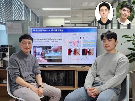
< Photo. The research team of the School of Electrical Engineering posed by the newly deveoped processor. (From center to the right) Professor Young-Gyu Yoon, Integrated Master's and Doctoral Program Students Seungjae Han and Hakcheon Jeong and Professor Shinhyun Choi >
- Professor Shinhyun Choi and Professor Young-Gyu Yoon’s Joint Research Team from the School of Electrical Engineering developed a computing chip that can learn, correct errors, and process AI tasks
- Equipping a computing chip with high-reliability memristor devices with self-error correction functions for real-time learning and image processing
Existing computer systems have separate data processing and storage devices, making them inefficient for processing complex data like AI. A KAIST research team has developed a memristor-based integrated system similar to the way our brain processes information. It is now ready for application in various devices including smart security cameras, allowing them to recognize suspicious activity immediately without having to rely on remote cloud servers, and medical devices with which it can help analyze health data in real time.
KAIST (President Kwang Hyung Lee) announced on the 17th of January that the joint research team of Professor Shinhyun Choi and Professor Young-Gyu Yoon of the School of Electrical Engineering has developed a next-generation neuromorphic semiconductor-based ultra-small computing chip that can learn and correct errors on its own.
< Figure 1. Scanning electron microscope (SEM) image of a computing chip equipped with a highly reliable selector-less 32×32 memristor crossbar array (left). Hardware system developed for real-time artificial intelligence implementation (right). >
What is special about this computing chip is that it can learn and correct errors that occur due to non-ideal characteristics that were difficult to solve in existing neuromorphic devices. For example, when processing a video stream, the chip learns to automatically separate a moving object from the background, and it becomes better at this task over time.
This self-learning ability has been proven by achieving accuracy comparable to ideal computer simulations in real-time image processing. The research team's main achievement is that it has completed a system that is both reliable and practical, beyond the development of brain-like components.
The research team has developed the world's first memristor-based integrated system that can adapt to immediate environmental changes, and has presented an innovative solution that overcomes the limitations of existing technology.
< Figure 2. Background and foreground separation results of an image containing non-ideal characteristics of memristor devices (left). Real-time image separation results through on-device learning using the memristor computing chip developed by our research team (right). >
At the heart of this innovation is a next-generation semiconductor device called a memristor*. The variable resistance characteristics of this device can replace the role of synapses in neural networks, and by utilizing it, data storage and computation can be performed simultaneously, just like our brain cells.
*Memristor: A compound word of memory and resistor, next-generation electrical device whose resistance value is determined by the amount and direction of charge that has flowed between the two terminals in the past.
The research team designed a highly reliable memristor that can precisely control resistance changes and developed an efficient system that excludes complex compensation processes through self-learning. This study is significant in that it experimentally verified the commercialization possibility of a next-generation neuromorphic semiconductor-based integrated system that supports real-time learning and inference.
This technology will revolutionize the way artificial intelligence is used in everyday devices, allowing AI tasks to be processed locally without relying on remote cloud servers, making them faster, more privacy-protected, and more energy-efficient.
“This system is like a smart workspace where everything is within arm’s reach instead of having to go back and forth between desks and file cabinets,” explained KAIST researchers Hakcheon Jeong and Seungjae Han, who led the development of this technology. “This is similar to the way our brain processes information, where everything is processed efficiently at once at one spot.”
The research was conducted with Hakcheon Jeong and Seungjae Han, the students of Integrated Master's and Doctoral Program at KAIST School of Electrical Engineering being the co-first authors, the results of which was published online in the international academic journal, Nature Electronics, on January 8, 2025.
*Paper title: Self-supervised video processing with self-calibration on an analogue computing platform based on a selector-less memristor array ( https://doi.org/10.1038/s41928-024-01318-6 )
This research was supported by the Next-Generation Intelligent Semiconductor Technology Development Project, Excellent New Researcher Project and PIM AI Semiconductor Core Technology Development Project of the National Research Foundation of Korea, and the Electronics and Telecommunications Research Institute Research and Development Support Project of the Institute of Information & communications Technology Planning & Evaluation.
2025.01.17 View 7344
KAIST Develops Neuromorphic Semiconductor Chip that Learns and Corrects Itself
< Photo. The research team of the School of Electrical Engineering posed by the newly deveoped processor. (From center to the right) Professor Young-Gyu Yoon, Integrated Master's and Doctoral Program Students Seungjae Han and Hakcheon Jeong and Professor Shinhyun Choi >
- Professor Shinhyun Choi and Professor Young-Gyu Yoon’s Joint Research Team from the School of Electrical Engineering developed a computing chip that can learn, correct errors, and process AI tasks
- Equipping a computing chip with high-reliability memristor devices with self-error correction functions for real-time learning and image processing
Existing computer systems have separate data processing and storage devices, making them inefficient for processing complex data like AI. A KAIST research team has developed a memristor-based integrated system similar to the way our brain processes information. It is now ready for application in various devices including smart security cameras, allowing them to recognize suspicious activity immediately without having to rely on remote cloud servers, and medical devices with which it can help analyze health data in real time.
KAIST (President Kwang Hyung Lee) announced on the 17th of January that the joint research team of Professor Shinhyun Choi and Professor Young-Gyu Yoon of the School of Electrical Engineering has developed a next-generation neuromorphic semiconductor-based ultra-small computing chip that can learn and correct errors on its own.
< Figure 1. Scanning electron microscope (SEM) image of a computing chip equipped with a highly reliable selector-less 32×32 memristor crossbar array (left). Hardware system developed for real-time artificial intelligence implementation (right). >
What is special about this computing chip is that it can learn and correct errors that occur due to non-ideal characteristics that were difficult to solve in existing neuromorphic devices. For example, when processing a video stream, the chip learns to automatically separate a moving object from the background, and it becomes better at this task over time.
This self-learning ability has been proven by achieving accuracy comparable to ideal computer simulations in real-time image processing. The research team's main achievement is that it has completed a system that is both reliable and practical, beyond the development of brain-like components.
The research team has developed the world's first memristor-based integrated system that can adapt to immediate environmental changes, and has presented an innovative solution that overcomes the limitations of existing technology.
< Figure 2. Background and foreground separation results of an image containing non-ideal characteristics of memristor devices (left). Real-time image separation results through on-device learning using the memristor computing chip developed by our research team (right). >
At the heart of this innovation is a next-generation semiconductor device called a memristor*. The variable resistance characteristics of this device can replace the role of synapses in neural networks, and by utilizing it, data storage and computation can be performed simultaneously, just like our brain cells.
*Memristor: A compound word of memory and resistor, next-generation electrical device whose resistance value is determined by the amount and direction of charge that has flowed between the two terminals in the past.
The research team designed a highly reliable memristor that can precisely control resistance changes and developed an efficient system that excludes complex compensation processes through self-learning. This study is significant in that it experimentally verified the commercialization possibility of a next-generation neuromorphic semiconductor-based integrated system that supports real-time learning and inference.
This technology will revolutionize the way artificial intelligence is used in everyday devices, allowing AI tasks to be processed locally without relying on remote cloud servers, making them faster, more privacy-protected, and more energy-efficient.
“This system is like a smart workspace where everything is within arm’s reach instead of having to go back and forth between desks and file cabinets,” explained KAIST researchers Hakcheon Jeong and Seungjae Han, who led the development of this technology. “This is similar to the way our brain processes information, where everything is processed efficiently at once at one spot.”
The research was conducted with Hakcheon Jeong and Seungjae Han, the students of Integrated Master's and Doctoral Program at KAIST School of Electrical Engineering being the co-first authors, the results of which was published online in the international academic journal, Nature Electronics, on January 8, 2025.
*Paper title: Self-supervised video processing with self-calibration on an analogue computing platform based on a selector-less memristor array ( https://doi.org/10.1038/s41928-024-01318-6 )
This research was supported by the Next-Generation Intelligent Semiconductor Technology Development Project, Excellent New Researcher Project and PIM AI Semiconductor Core Technology Development Project of the National Research Foundation of Korea, and the Electronics and Telecommunications Research Institute Research and Development Support Project of the Institute of Information & communications Technology Planning & Evaluation.
2025.01.17 View 7344 -
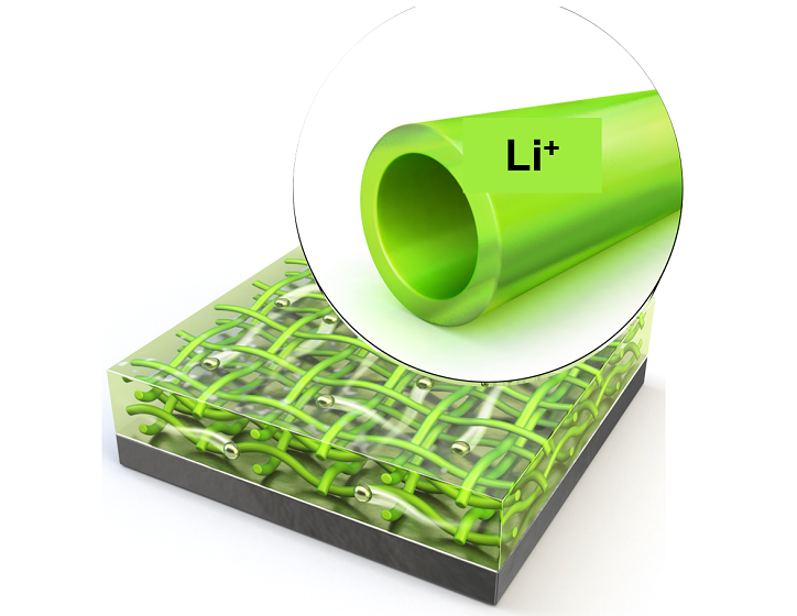 KAIST Extends Lithium Metal Battery Lifespan by 750% Using Water
Lithium metal, a next-generation anode material, has been highlighted for overcoming the performance limitations of commercial batteries. However, issues inherent to lithium metal have caused shortened battery lifespans and increased fire risks. KAIST researchers have achieved a world-class breakthrough by extending the lifespan of lithium metal anodes by approximately 750% only using water.
KAIST (represented by President Kwang Hyung Lee) announced on the 2nd of December that Professor Il-Doo Kim from the Department of Materials Science and Engineering, in collaboration with Professor Jiyoung Lee from Ajou University, successfully stabilized lithium growth and significantly enhanced the lifespan of next-generation lithium metal batteries using eco-friendly hollow nanofibers as protective layers.
Conventional protective layer technologies, which involve applying a surface coating onto lithium metal in order to create an artificial interface with the electrolyte, have relied on toxic processes and expensive materials, with limited improvements in the lifespan of lithium metal anodes.
< Figure 1. Schematic illustration of the fabrication process of the newly developed protective membrane by eco-friendly electrospinning process using water >
To address these limitations, Professor Kim’s team proposed a hollow nanofiber protective layer capable of controlling lithium-ion growth through both physical and chemical means. This protective layer was manufactured through an environmentally friendly electrospinning process* using guar gum** extracted from plants as the primary material and utilizing water as the sole solvent.
*Electrospinning process: A method where polymer solutions are subjected to an electric field, producing continuous fibers with diameters ranging from tens of nanometers to several micrometers.
**Guar gum: A natural polymer extracted from guar beans, composed mainly of monosaccharides. Its oxidized functional groups regulate interactions with lithium ions.
< Figure 2. Physical and chemical control of Lithium dendrite by the newly developed protective membrane >
The nanofiber protective layer effectively controlled reversible chemical reactions between the electrolyte and lithium ions. The hollow spaces within the fibers suppressed the random accumulation of lithium ions on the metal surface, stabilizing the interface between the lithium metal surface and the electrolyte.
< Figure 3. Performance of Lithium metal battery full cells with the newly developed protective membrane >
As a result, the lithium metal anodes with this protective layer demonstrated approximately a 750% increase in lifespan compared to conventional lithium metal anodes. The battery retained 93.3% of its capacity even after 300 charge-discharge cycles, achieving world-class performance.
The researchers also verified that this natural protective layer decomposes entirely within about a month in soil, proving its eco-friendly nature throughout the manufacturing and disposal process.
< Figure 4. Excellent decomposition rate of the newly developed protective membrane >
Professor Il-Doo Kim explained, “By leveraging both physical and chemical protective functions, we were able to guide reversible reactions between lithium metal and the electrolyte more effectively and suppress dendrite growth, resulting in lithium metal anodes with unprecedented lifespan characteristics.”
He added, “As the environmental burden caused by battery production and disposal becomes a pressing issue due to surging battery demand, this water-based manufacturing method with biodegradable properties will significantly contribute to the commercialization of next-generation eco-friendly batteries.”
This study was led by Dr. Jiyoung Lee (now a professor in the Department of Chemical Engineering at Ajou University) and Dr. Hyunsub Song (currently at Samsung Electronics), both graduates of KAIST’s Department of Materials Science and Engineering. The findings were published as a front cover article in Advanced Materials, Volume 36, Issue 47, on November 21.
(Paper title: “Overcoming Chemical and Mechanical Instabilities in Lithium Metal Anodes with Sustainable and Eco-Friendly Artificial SEI Layer”)
The research was supported by the KAIST-LG Energy Solution Frontier Research Lab (FRL), the Alchemist Project funded by the Ministry of Trade, Industry and Energy, and the Top-Tier Research Support Program from the Ministry of Science and ICT.
2024.12.12 View 6500
KAIST Extends Lithium Metal Battery Lifespan by 750% Using Water
Lithium metal, a next-generation anode material, has been highlighted for overcoming the performance limitations of commercial batteries. However, issues inherent to lithium metal have caused shortened battery lifespans and increased fire risks. KAIST researchers have achieved a world-class breakthrough by extending the lifespan of lithium metal anodes by approximately 750% only using water.
KAIST (represented by President Kwang Hyung Lee) announced on the 2nd of December that Professor Il-Doo Kim from the Department of Materials Science and Engineering, in collaboration with Professor Jiyoung Lee from Ajou University, successfully stabilized lithium growth and significantly enhanced the lifespan of next-generation lithium metal batteries using eco-friendly hollow nanofibers as protective layers.
Conventional protective layer technologies, which involve applying a surface coating onto lithium metal in order to create an artificial interface with the electrolyte, have relied on toxic processes and expensive materials, with limited improvements in the lifespan of lithium metal anodes.
< Figure 1. Schematic illustration of the fabrication process of the newly developed protective membrane by eco-friendly electrospinning process using water >
To address these limitations, Professor Kim’s team proposed a hollow nanofiber protective layer capable of controlling lithium-ion growth through both physical and chemical means. This protective layer was manufactured through an environmentally friendly electrospinning process* using guar gum** extracted from plants as the primary material and utilizing water as the sole solvent.
*Electrospinning process: A method where polymer solutions are subjected to an electric field, producing continuous fibers with diameters ranging from tens of nanometers to several micrometers.
**Guar gum: A natural polymer extracted from guar beans, composed mainly of monosaccharides. Its oxidized functional groups regulate interactions with lithium ions.
< Figure 2. Physical and chemical control of Lithium dendrite by the newly developed protective membrane >
The nanofiber protective layer effectively controlled reversible chemical reactions between the electrolyte and lithium ions. The hollow spaces within the fibers suppressed the random accumulation of lithium ions on the metal surface, stabilizing the interface between the lithium metal surface and the electrolyte.
< Figure 3. Performance of Lithium metal battery full cells with the newly developed protective membrane >
As a result, the lithium metal anodes with this protective layer demonstrated approximately a 750% increase in lifespan compared to conventional lithium metal anodes. The battery retained 93.3% of its capacity even after 300 charge-discharge cycles, achieving world-class performance.
The researchers also verified that this natural protective layer decomposes entirely within about a month in soil, proving its eco-friendly nature throughout the manufacturing and disposal process.
< Figure 4. Excellent decomposition rate of the newly developed protective membrane >
Professor Il-Doo Kim explained, “By leveraging both physical and chemical protective functions, we were able to guide reversible reactions between lithium metal and the electrolyte more effectively and suppress dendrite growth, resulting in lithium metal anodes with unprecedented lifespan characteristics.”
He added, “As the environmental burden caused by battery production and disposal becomes a pressing issue due to surging battery demand, this water-based manufacturing method with biodegradable properties will significantly contribute to the commercialization of next-generation eco-friendly batteries.”
This study was led by Dr. Jiyoung Lee (now a professor in the Department of Chemical Engineering at Ajou University) and Dr. Hyunsub Song (currently at Samsung Electronics), both graduates of KAIST’s Department of Materials Science and Engineering. The findings were published as a front cover article in Advanced Materials, Volume 36, Issue 47, on November 21.
(Paper title: “Overcoming Chemical and Mechanical Instabilities in Lithium Metal Anodes with Sustainable and Eco-Friendly Artificial SEI Layer”)
The research was supported by the KAIST-LG Energy Solution Frontier Research Lab (FRL), the Alchemist Project funded by the Ministry of Trade, Industry and Energy, and the Top-Tier Research Support Program from the Ministry of Science and ICT.
2024.12.12 View 6500 -
 A KAIST Team Develops Face-Conforming LED Mask Showing 340% Improved Efficacy in Deep Skin Elasticity
- A KAIST research team led by Professor Keon Jae Lee has developed a deep skin-stimulating LED mask which has been verified in clinical trials to improve dermis elasticity by 340%.
< Figure 1. Overall concept of face-fit surface-lighting micro-LEDs (FSLED) mask. a. Optical image of the FSLED mask showing uniform surface-lighting. schematic illustration of the FSLED mask. The 2D to 3D transformation procedure b. Difference in cosmetic effect on deep skin elasticity, wrinkles, and sagging between FSLED mask and CLED mask. (improvement percentage in eight weeks) >
Conventional LED masks, with their rigid design, fail to conform closely to the skin's contours. This limitation causes substantial light reflection, with up to 90% reflected over a distance of 2 cm, reducing light penetration and limiting stimulation of the deep skin layers essential for effective skin rejuvenation.
To address these challenges, Professor Lee's team developed a face-conforming surface lighting micro-LED (FSLED) mask, which can provide uniform photostimulation to the dermis. The key technology lies in the mask's ability to deliver uniform light to deep skin tissues while maintaining a conformal skin attachment. This is achieved through a 3D origami structure, integrated with 3,770 micro-LEDs and flexible surface light-diffusion layer, minimizing the gaps between the light source and the skin.
In clinical trials involving 33 participants, the FSLED mask demonstrated a 340% improvement in deep skin elasticity compared to conventional LED masks, proving its efficacy in significantly reducing skin wrinkles, sagging and aging.
Professor Keon Jae Lee said, “The FSLED mask provides cosmetic benefits to the entire facial dermis without the side effects of low-temperature burns, making home-care anti-aging treatment that enhances the quality of human life possible. The product is being manufactured by Fronics, KAIST startup company, and will be distributed globally through Amorepacific's network, with sales starting in November.”
This result titled “Clinical Validation of Face-fit Surface-lighting Micro Light-emitting Diode Mask for Skin Anti-aging Treatment”, in which Min Seo Kim, a student of the Master-Doctorate integrated program, and Jaehun An, a Ph.D. candidate, in the Department of Materials Science and Engineering of KAIST, took part as co-first authors, was published in Advanced Materials on October 22nd, 2024 (DOI: 10.1002/adma.202411651).
Introductory Video: Face-conforming surface LED mask for skin anti-aging ( https://www.youtube.com/watch?v=kSccLwx8N_w )
2024.10.29 View 7309
A KAIST Team Develops Face-Conforming LED Mask Showing 340% Improved Efficacy in Deep Skin Elasticity
- A KAIST research team led by Professor Keon Jae Lee has developed a deep skin-stimulating LED mask which has been verified in clinical trials to improve dermis elasticity by 340%.
< Figure 1. Overall concept of face-fit surface-lighting micro-LEDs (FSLED) mask. a. Optical image of the FSLED mask showing uniform surface-lighting. schematic illustration of the FSLED mask. The 2D to 3D transformation procedure b. Difference in cosmetic effect on deep skin elasticity, wrinkles, and sagging between FSLED mask and CLED mask. (improvement percentage in eight weeks) >
Conventional LED masks, with their rigid design, fail to conform closely to the skin's contours. This limitation causes substantial light reflection, with up to 90% reflected over a distance of 2 cm, reducing light penetration and limiting stimulation of the deep skin layers essential for effective skin rejuvenation.
To address these challenges, Professor Lee's team developed a face-conforming surface lighting micro-LED (FSLED) mask, which can provide uniform photostimulation to the dermis. The key technology lies in the mask's ability to deliver uniform light to deep skin tissues while maintaining a conformal skin attachment. This is achieved through a 3D origami structure, integrated with 3,770 micro-LEDs and flexible surface light-diffusion layer, minimizing the gaps between the light source and the skin.
In clinical trials involving 33 participants, the FSLED mask demonstrated a 340% improvement in deep skin elasticity compared to conventional LED masks, proving its efficacy in significantly reducing skin wrinkles, sagging and aging.
Professor Keon Jae Lee said, “The FSLED mask provides cosmetic benefits to the entire facial dermis without the side effects of low-temperature burns, making home-care anti-aging treatment that enhances the quality of human life possible. The product is being manufactured by Fronics, KAIST startup company, and will be distributed globally through Amorepacific's network, with sales starting in November.”
This result titled “Clinical Validation of Face-fit Surface-lighting Micro Light-emitting Diode Mask for Skin Anti-aging Treatment”, in which Min Seo Kim, a student of the Master-Doctorate integrated program, and Jaehun An, a Ph.D. candidate, in the Department of Materials Science and Engineering of KAIST, took part as co-first authors, was published in Advanced Materials on October 22nd, 2024 (DOI: 10.1002/adma.202411651).
Introductory Video: Face-conforming surface LED mask for skin anti-aging ( https://www.youtube.com/watch?v=kSccLwx8N_w )
2024.10.29 View 7309 -
 KAIST Develops a Fire-risk Free Self-Powered Hydrogen Production System
KAIST researchers have developed a new hydrogen production system that overcomes the current limitations of green hydrogen production. By using a water-splitting system with an aqueous electrolyte, this system is expected to block fire risks and enable stable hydrogen production.
KAIST (represented by President Kwang Hyung Lee) announced on the 22nd of October that a research team led by Professor Jeung Ku Kang from the Department of Materials Science and Engineering developed a self-powered hydrogen production system based on a high-performance zinc-air battery*.
*Zinc-air battery: A primary battery that absorbs oxygen from the air and uses it as an oxidant. Its advantage is long life, but its low electromotive force is a disadvantage.
Hydrogen (H₂) is a key raw material for synthesizing high-value-added substances, and it is gaining attention as a clean fuel with an energy density (142 MJ/kg) more than three times higher than traditional fossil fuels (gasoline, diesel, etc.). However, most current hydrogen production methods impose environmental burden as they emit carbon dioxide (CO₂).
While green hydrogen can be produced by splitting water using renewable energy sources such as solar cells and wind power, these sources are subject to irregular power generation due to weather and temperature fluctuations, leading to low water-splitting efficiency.
To overcome this, air batteries that can emit sufficient voltage (greater than 1.23V) for water splitting have been gaining attention. However, achieving sufficient capacity requires expensive precious metal catalysts and the performance of the catalyst materials becomes significantly degraded during prolonged charge and discharge cycles. Thus, it is essential to develop catalysts that are effective for the water-splitting reactions (oxygen and hydrogen evolution) and materials that can stabilize the repeated charge and discharge reactions (oxygen reduction and evolution) in zinc-air battery electrodes.
In response, Professor Kang's research team proposed a method to synthesize a non-precious metal catalyst material (G-SHELL) that is effective for three different catalytic reactions (oxygen evolution, hydrogen evolution, and oxygen reduction) by growing nano-sized, metal-organic frameworks on graphene oxide.
The team incorporated the developed catalyst material into the air cathode of a zinc-air battery, confirming that it achieved approximately five times higher energy density (797Wh/kg), high power characteristics (275.8mW/cm²), and long-term stability even under repeated charge and discharge conditions compared to conventional batteries.
Additionally, the zinc-air battery, which operates using an aqueous electrolyte, is safe from fire risks. It is expected that this system can be applied as a next-generation energy storage device when linked with water electrolysis systems, offering an environmentally friendly method for hydrogen production.
< Figure 1. Illustrations of a trifunctional graphene-sandwiched heterojunction-embedded layered lattice (G-SHELL) structure. Schematic representation of a) synthesis procedures of G-SHELL from a zeolitic imidazole framework, b) hollow core-layered shell structure with trifunctional sites for oxygen reduction evolution (ORR), oxygen evolution reaction (OER), and hydrogen evolution reaction (HER), and c) heterojunctions, eterojunction-induced internal electric fields, and the corresponding band structure. >
Professor Kang explained, "By developing a catalyst material with high activity and durability for three different electrochemical catalytic reactions at low temperatures using simple methods, the self-powered hydrogen production system we implemented based on zinc-air batteries presents a new breakthrough to overcome the current limitations of green hydrogen production."
<Figure 2. Electrochemical performance of a ZAB-driven water-splitting cell with G-SHELL. Diagram of a self-driven water-splitting cell integrated by combining a ZAB with an alkaline water electrolyzer.>
PhD candidate Dong Won Kim and Jihoon Kim, a master's student in the Department of Materials Science and Engineering at KAIST, were co-first authors of this research, which was published in the international journal Advanced Science on September 17th in the multidisciplinary field of materials science. (Paper Title: “Trifunctional Graphene-Sandwiched Heterojunction-Embedded Layered Lattice Electrocatalyst for High Performance in Zn-Air Battery-Driven Water Splitting”)
This research was supported by the Nano and Material Technology Development Program of the Ministry of Science and ICT and the National Research Foundation of Korea’s Future Technology Research Laboratory.
2024.10.22 View 5803
KAIST Develops a Fire-risk Free Self-Powered Hydrogen Production System
KAIST researchers have developed a new hydrogen production system that overcomes the current limitations of green hydrogen production. By using a water-splitting system with an aqueous electrolyte, this system is expected to block fire risks and enable stable hydrogen production.
KAIST (represented by President Kwang Hyung Lee) announced on the 22nd of October that a research team led by Professor Jeung Ku Kang from the Department of Materials Science and Engineering developed a self-powered hydrogen production system based on a high-performance zinc-air battery*.
*Zinc-air battery: A primary battery that absorbs oxygen from the air and uses it as an oxidant. Its advantage is long life, but its low electromotive force is a disadvantage.
Hydrogen (H₂) is a key raw material for synthesizing high-value-added substances, and it is gaining attention as a clean fuel with an energy density (142 MJ/kg) more than three times higher than traditional fossil fuels (gasoline, diesel, etc.). However, most current hydrogen production methods impose environmental burden as they emit carbon dioxide (CO₂).
While green hydrogen can be produced by splitting water using renewable energy sources such as solar cells and wind power, these sources are subject to irregular power generation due to weather and temperature fluctuations, leading to low water-splitting efficiency.
To overcome this, air batteries that can emit sufficient voltage (greater than 1.23V) for water splitting have been gaining attention. However, achieving sufficient capacity requires expensive precious metal catalysts and the performance of the catalyst materials becomes significantly degraded during prolonged charge and discharge cycles. Thus, it is essential to develop catalysts that are effective for the water-splitting reactions (oxygen and hydrogen evolution) and materials that can stabilize the repeated charge and discharge reactions (oxygen reduction and evolution) in zinc-air battery electrodes.
In response, Professor Kang's research team proposed a method to synthesize a non-precious metal catalyst material (G-SHELL) that is effective for three different catalytic reactions (oxygen evolution, hydrogen evolution, and oxygen reduction) by growing nano-sized, metal-organic frameworks on graphene oxide.
The team incorporated the developed catalyst material into the air cathode of a zinc-air battery, confirming that it achieved approximately five times higher energy density (797Wh/kg), high power characteristics (275.8mW/cm²), and long-term stability even under repeated charge and discharge conditions compared to conventional batteries.
Additionally, the zinc-air battery, which operates using an aqueous electrolyte, is safe from fire risks. It is expected that this system can be applied as a next-generation energy storage device when linked with water electrolysis systems, offering an environmentally friendly method for hydrogen production.
< Figure 1. Illustrations of a trifunctional graphene-sandwiched heterojunction-embedded layered lattice (G-SHELL) structure. Schematic representation of a) synthesis procedures of G-SHELL from a zeolitic imidazole framework, b) hollow core-layered shell structure with trifunctional sites for oxygen reduction evolution (ORR), oxygen evolution reaction (OER), and hydrogen evolution reaction (HER), and c) heterojunctions, eterojunction-induced internal electric fields, and the corresponding band structure. >
Professor Kang explained, "By developing a catalyst material with high activity and durability for three different electrochemical catalytic reactions at low temperatures using simple methods, the self-powered hydrogen production system we implemented based on zinc-air batteries presents a new breakthrough to overcome the current limitations of green hydrogen production."
<Figure 2. Electrochemical performance of a ZAB-driven water-splitting cell with G-SHELL. Diagram of a self-driven water-splitting cell integrated by combining a ZAB with an alkaline water electrolyzer.>
PhD candidate Dong Won Kim and Jihoon Kim, a master's student in the Department of Materials Science and Engineering at KAIST, were co-first authors of this research, which was published in the international journal Advanced Science on September 17th in the multidisciplinary field of materials science. (Paper Title: “Trifunctional Graphene-Sandwiched Heterojunction-Embedded Layered Lattice Electrocatalyst for High Performance in Zn-Air Battery-Driven Water Splitting”)
This research was supported by the Nano and Material Technology Development Program of the Ministry of Science and ICT and the National Research Foundation of Korea’s Future Technology Research Laboratory.
2024.10.22 View 5803 -
 KAIST Develops Thread-like, Flexible Thermoelectric Materials Applicable in Extreme Environments
A team of Korean researchers developed a thermoelectric material that can be used in wearable devices, such as smart clothing, and while maintaining stable thermal energy performance even in extreme environments. It has dramatically resolved the dilemma of striking the balance between achieving good performance and the mechanical flexibility of thermoelectric materials, which has been a long-standing challenge in the field of thermoelectric materials, and has also proven the possibility of commercialization.
KAIST (President Kwang-Hyung Lee) announced on the 21st that a joint research team of Professor Yeon Sik Jung of the Department of Materials Science and Engineering and Professor Inkyu Park of the Department of Mechanical Engineering, in collaboration with the research teams of Professor Min-Wook Oh of Hanbat National University (President Yong Jun Oh) and Dr. Jun-Ho Jeong of the Korea Institute of Machinery and Materials (President Seoghyun Ryu), have successfully developed ‘bismuth telluride (Bi2Te3) thermoelectric fibers,’ an innovative energy harvesting solution for next-generation flexible electronic devices.
Thermoelectric materials are materials that generate voltage when there is a temperature difference and convert thermal energy into electrical energy. Currently, about 70% of energy being lost as wasted heat, so due attention is being given to research on these as sustainable energy materials that can recover and harvesting energy from this waste heat.
Most of the heat sources around us are curved, such as the human body, vehicle exhaust pipes, and cooling fins. Inorganic thermoelectric materials based on ceramic materials boast high thermoelectric performance, but they are fragile and difficult to produce in curved shapes. On the other hand, flexible thermoelectric materials using existing polymer binders can be applied to surfaces of various shapes, but their performance was limited due to the low electrical conductivity and high thermal resistance of the polymer.
Existing flexible thermoelectric materials contain polymer additives, but the inorganic thermoelectric material developed by the research team is not flexible, so they overcame these limitations by twisting nano ribbons instead of additives to produce a thread-shaped thermoelectric material. Inspired by the flexibility of inorganic nano ribbons, the research team used a nanomold-based electron beam deposition technique to continuously deposit nano ribbons and then twisted them into a thread shape to create bismuth telluride (Bi2Te3) inorganic thermoelectric fibers.
These inorganic thermoelectric fibers have higher bending strength than existing thermoelectric materials, and showed almost no change in electrical properties even after repeated bending and tensile tests of more than 1,000 times. The thermoelectric device created by the research team generates electricity using temperature differences, and if clothes are made with fiber-type thermoelectric devices, electricity can be generated from body temperature to operate other electronic devices.
< Figure 1. Schematic diagram and actual image of the all-inorganic flexible thermoelectric yarn made without polymer additives >
In fact, the possibility of commercialization was proven through a demonstration of collecting energy by embedding thermoelectric fibers in life jackets or clothing. In addition, it opened up the possibility of building a high-efficiency energy harvesting system that recycles waste heat by utilizing the temperature difference between the hot fluid inside a pipe and the cold air outside in industrial settings.
Professor Yeon Sik Jung said, "The inorganic flexible thermoelectric material developed in this study can be used in wearable devices such as smart clothing, and it can maintain stable performance even in extreme environments, so it has a high possibility of being commercialized through additional research in the future." Professor Inkyu Park also emphasized, "This technology will become the core of next-generation energy harvesting technology, and it is expected to play an important role in various fields from waste heat utilization in industrial sites to personal wearable self-power generation devices."
This study, in which Hanhwi Jang, a Ph.D. student at KAIST's Department of Materials Science and Engineering, Professor Junseong Ahn of Korea University, Sejong Campus, and Dr. Yongrok Jeong of Korea Atomic Energy Research Institute contributed equally as joint first authors, was published in the online edition of the international academic journal Advanced Materials on September 17, and was selected as the back-cover paper in recognition of its excellence. (Paper title: Flexible All-Inorganic Thermoelectric Yarns)
Meanwhile, this study was conducted through the Mid-career Researcher Support Program and the Future Materials Discovery Program of the National Research Foundation of Korea, and the support from the Global Bio-Integrated Materials Center, the Ministry of Trade, Industry and Energy, and the Korea Institute of Industrial Technology Evaluation and Planning (KEIT) upon the support by the Ministry of Science and ICT.
2024.10.21 View 4581
KAIST Develops Thread-like, Flexible Thermoelectric Materials Applicable in Extreme Environments
A team of Korean researchers developed a thermoelectric material that can be used in wearable devices, such as smart clothing, and while maintaining stable thermal energy performance even in extreme environments. It has dramatically resolved the dilemma of striking the balance between achieving good performance and the mechanical flexibility of thermoelectric materials, which has been a long-standing challenge in the field of thermoelectric materials, and has also proven the possibility of commercialization.
KAIST (President Kwang-Hyung Lee) announced on the 21st that a joint research team of Professor Yeon Sik Jung of the Department of Materials Science and Engineering and Professor Inkyu Park of the Department of Mechanical Engineering, in collaboration with the research teams of Professor Min-Wook Oh of Hanbat National University (President Yong Jun Oh) and Dr. Jun-Ho Jeong of the Korea Institute of Machinery and Materials (President Seoghyun Ryu), have successfully developed ‘bismuth telluride (Bi2Te3) thermoelectric fibers,’ an innovative energy harvesting solution for next-generation flexible electronic devices.
Thermoelectric materials are materials that generate voltage when there is a temperature difference and convert thermal energy into electrical energy. Currently, about 70% of energy being lost as wasted heat, so due attention is being given to research on these as sustainable energy materials that can recover and harvesting energy from this waste heat.
Most of the heat sources around us are curved, such as the human body, vehicle exhaust pipes, and cooling fins. Inorganic thermoelectric materials based on ceramic materials boast high thermoelectric performance, but they are fragile and difficult to produce in curved shapes. On the other hand, flexible thermoelectric materials using existing polymer binders can be applied to surfaces of various shapes, but their performance was limited due to the low electrical conductivity and high thermal resistance of the polymer.
Existing flexible thermoelectric materials contain polymer additives, but the inorganic thermoelectric material developed by the research team is not flexible, so they overcame these limitations by twisting nano ribbons instead of additives to produce a thread-shaped thermoelectric material. Inspired by the flexibility of inorganic nano ribbons, the research team used a nanomold-based electron beam deposition technique to continuously deposit nano ribbons and then twisted them into a thread shape to create bismuth telluride (Bi2Te3) inorganic thermoelectric fibers.
These inorganic thermoelectric fibers have higher bending strength than existing thermoelectric materials, and showed almost no change in electrical properties even after repeated bending and tensile tests of more than 1,000 times. The thermoelectric device created by the research team generates electricity using temperature differences, and if clothes are made with fiber-type thermoelectric devices, electricity can be generated from body temperature to operate other electronic devices.
< Figure 1. Schematic diagram and actual image of the all-inorganic flexible thermoelectric yarn made without polymer additives >
In fact, the possibility of commercialization was proven through a demonstration of collecting energy by embedding thermoelectric fibers in life jackets or clothing. In addition, it opened up the possibility of building a high-efficiency energy harvesting system that recycles waste heat by utilizing the temperature difference between the hot fluid inside a pipe and the cold air outside in industrial settings.
Professor Yeon Sik Jung said, "The inorganic flexible thermoelectric material developed in this study can be used in wearable devices such as smart clothing, and it can maintain stable performance even in extreme environments, so it has a high possibility of being commercialized through additional research in the future." Professor Inkyu Park also emphasized, "This technology will become the core of next-generation energy harvesting technology, and it is expected to play an important role in various fields from waste heat utilization in industrial sites to personal wearable self-power generation devices."
This study, in which Hanhwi Jang, a Ph.D. student at KAIST's Department of Materials Science and Engineering, Professor Junseong Ahn of Korea University, Sejong Campus, and Dr. Yongrok Jeong of Korea Atomic Energy Research Institute contributed equally as joint first authors, was published in the online edition of the international academic journal Advanced Materials on September 17, and was selected as the back-cover paper in recognition of its excellence. (Paper title: Flexible All-Inorganic Thermoelectric Yarns)
Meanwhile, this study was conducted through the Mid-career Researcher Support Program and the Future Materials Discovery Program of the National Research Foundation of Korea, and the support from the Global Bio-Integrated Materials Center, the Ministry of Trade, Industry and Energy, and the Korea Institute of Industrial Technology Evaluation and Planning (KEIT) upon the support by the Ministry of Science and ICT.
2024.10.21 View 4581 -
 KAIST Develops Sodium Battery Capable of Rapid Charging in Just a Few Seconds
Sodium (Na), which is over 500 times more abundant than lithium (Li), has recently garnered significant attention for its potential in sodium-ion battery technologies. However, existing sodium-ion batteries face fundamental limitations, including lower power output, constrained storage properties, and longer charging times, necessitating the development of next-generation energy storage materials.
On the 11th of April, KAIST (represented by President Kwang Hyung Lee) announced that a research team led by Professor Jeung Ku Kang from the Department of Materials Science and Engineering had developed a high-energy, high-power hybrid sodium-ion battery capable of rapid charging.
The innovative hybrid energy storage system integrates anode materials typically used in batteries with cathodes suitable for supercapacitors. This combination allows the device to achieve both high storage capacities and rapid charge-discharge rates, positioning it as a viable next-generation alternative to lithium-ion batteries.
However, the development of a hybrid battery with high energy and high power density requires an improvement to the slow energy storage rate of battery-type anodes as well as the enhancement of the relatively low capacity of supercapacitor-type cathode materials.
< Figure 1. Schematic synthetic procedures of high-capacity/high-rate anode and cathode materials for a sodium-ion hybrid energy storages (SIHES) and their proposed energy storage mechanisms. Synthetic procedures for (a) ultrafine iron sulfide-embedded S-doped carbon/graphene (FS/C/G) anode and (b) zeolitic imidazolate framework-derived porous carbon (ZDPC) cathode materials. (c) Proposed energy storage mechanisms of Na+ ions in FS/C/G anode and ClO-4 ions in ZDPC cathode for an SIHES. >
To account for this, Professor Kang's team utilized two distinct metal-organic frameworks for the optimized synthesis of hybrid batteries. This approach led to the development of an anode material with improved kinetics through the inclusion of fine active materials in porous carbon derived from metal-organic frameworks. Additionally, a high-capacity cathode material was synthesized, and the combination of the cathode and anode materials allowed for the development of a sodium-ion storage system optimizing the balance and minimizing the disparities in energy storage rates between the electrodes.
The assembled full cell, comprising the newly developed anode and cathode, forms a high-performance hybrid sodium-ion energy storage device. This device surpasses the energy density of commercial lithium-ion batteries and exhibits the characteristics of supercapacitors' power density. It is expected to be suitable for rapid charging applications ranging from electric vehicles to smart electronic devices and aerospace technologies.
< Figure 2. Electrochemical characterizations of FS/C/G-20//ZDPC SIHES full cells (left). Ragone plots for FS/C/G-20//ZDPC (this work) and other previously reported sodium-ion electrochemical energy storage devices (right). >
Professor Kang noted that the hybrid sodium-ion energy storage device, capable of rapid charging and achieving an energy density of 247 Wh/kg and a power density of 34,748 W/kg, represents a breakthrough in overcoming the current limitations of energy storage systems. He anticipates broader applications across various electronic devices, including electric vehicles.
This research, co-authored by KAIST doctoral candidates Jong Hui Choi and Dong Won Kim, was published in the international journal Energy Storage Materials on March 29 with the title "Low-crystallinity conductive multivalence iron sulfide-embedded S-doped anode and high-surface-area O-doped cathode of 3D porous N-rich graphitic carbon frameworks for high-performance sodium-ion hybrid energy storages."
The study was conducted with support from the Ministry of Science and ICT and the National Research Foundation of Korea through the Nanomaterial Technology Development Project.
2024.04.18 View 18481
KAIST Develops Sodium Battery Capable of Rapid Charging in Just a Few Seconds
Sodium (Na), which is over 500 times more abundant than lithium (Li), has recently garnered significant attention for its potential in sodium-ion battery technologies. However, existing sodium-ion batteries face fundamental limitations, including lower power output, constrained storage properties, and longer charging times, necessitating the development of next-generation energy storage materials.
On the 11th of April, KAIST (represented by President Kwang Hyung Lee) announced that a research team led by Professor Jeung Ku Kang from the Department of Materials Science and Engineering had developed a high-energy, high-power hybrid sodium-ion battery capable of rapid charging.
The innovative hybrid energy storage system integrates anode materials typically used in batteries with cathodes suitable for supercapacitors. This combination allows the device to achieve both high storage capacities and rapid charge-discharge rates, positioning it as a viable next-generation alternative to lithium-ion batteries.
However, the development of a hybrid battery with high energy and high power density requires an improvement to the slow energy storage rate of battery-type anodes as well as the enhancement of the relatively low capacity of supercapacitor-type cathode materials.
< Figure 1. Schematic synthetic procedures of high-capacity/high-rate anode and cathode materials for a sodium-ion hybrid energy storages (SIHES) and their proposed energy storage mechanisms. Synthetic procedures for (a) ultrafine iron sulfide-embedded S-doped carbon/graphene (FS/C/G) anode and (b) zeolitic imidazolate framework-derived porous carbon (ZDPC) cathode materials. (c) Proposed energy storage mechanisms of Na+ ions in FS/C/G anode and ClO-4 ions in ZDPC cathode for an SIHES. >
To account for this, Professor Kang's team utilized two distinct metal-organic frameworks for the optimized synthesis of hybrid batteries. This approach led to the development of an anode material with improved kinetics through the inclusion of fine active materials in porous carbon derived from metal-organic frameworks. Additionally, a high-capacity cathode material was synthesized, and the combination of the cathode and anode materials allowed for the development of a sodium-ion storage system optimizing the balance and minimizing the disparities in energy storage rates between the electrodes.
The assembled full cell, comprising the newly developed anode and cathode, forms a high-performance hybrid sodium-ion energy storage device. This device surpasses the energy density of commercial lithium-ion batteries and exhibits the characteristics of supercapacitors' power density. It is expected to be suitable for rapid charging applications ranging from electric vehicles to smart electronic devices and aerospace technologies.
< Figure 2. Electrochemical characterizations of FS/C/G-20//ZDPC SIHES full cells (left). Ragone plots for FS/C/G-20//ZDPC (this work) and other previously reported sodium-ion electrochemical energy storage devices (right). >
Professor Kang noted that the hybrid sodium-ion energy storage device, capable of rapid charging and achieving an energy density of 247 Wh/kg and a power density of 34,748 W/kg, represents a breakthrough in overcoming the current limitations of energy storage systems. He anticipates broader applications across various electronic devices, including electric vehicles.
This research, co-authored by KAIST doctoral candidates Jong Hui Choi and Dong Won Kim, was published in the international journal Energy Storage Materials on March 29 with the title "Low-crystallinity conductive multivalence iron sulfide-embedded S-doped anode and high-surface-area O-doped cathode of 3D porous N-rich graphitic carbon frameworks for high-performance sodium-ion hybrid energy storages."
The study was conducted with support from the Ministry of Science and ICT and the National Research Foundation of Korea through the Nanomaterial Technology Development Project.
2024.04.18 View 18481 -
 KAIST researchers developed a novel ultra-low power memory for neuromorphic computing
A team of Korean researchers is making headlines by developing a new memory device that can be used to replace existing memory or used in implementing neuromorphic computing for next-generation artificial intelligence hardware for its low processing costs and its ultra-low power consumption.
KAIST (President Kwang-Hyung Lee) announced on April 4th that Professor Shinhyun Choi's research team in the School of Electrical Engineering has developed a next-generation phase change memory* device featuring ultra-low-power consumption that can replace DRAM and NAND flash memory.
☞ Phase change memory: A memory device that stores and/or processes information by changing the crystalline states of materials to be amorphous or crystalline using heat, thereby changing its resistance state.
Existing phase change memory has the problems such as expensive fabrication process for making highly scaled device and requiring substantial amount of power for operation. To solve these problems, Professor Choi’s research team developed an ultra-low power phase change memory device by electrically forming a very small nanometer (nm) scale phase changeable filament without expensive fabrication processes. This new development has the groundbreaking advantage of not only having a very low processing cost but also of enabling operating with ultra-low power consumption.
DRAM, one of the most popularly used memory, is very fast, but has volatile characteristics in which data disappears when the power is turned off. NAND flash memory, a storage device, has relatively slow read/write speeds, but it has non-volatile characteristic that enables it to preserve the data even when the power is cut off.
Phase change memory, on the other hand, combines the advantages of both DRAM and NAND flash memory, offering high speed and non-volatile characteristics. For this reason, phase change memory is being highlighted as the next-generation memory that can replace existing memory, and is being actively researched as a memory technology or neuromorphic computing technology that mimics the human brain.
However, conventional phase change memory devices require a substantial amount of power to operate, making it difficult to make practical large-capacity memory products or realize a neuromorphic computing system. In order to maximize the thermal efficiency for memory device operation, previous research efforts focused on reducing the power consumption by shrinking the physical size of the device through the use of the state-of-the-art lithography technologies, but they were met with limitations in terms of practicality as the degree of improvement in power consumption was minimal whereas the cost and the difficulty of fabrication increased with each improvement.
In order to solve the power consumption problem of phase change memory, Professor Shinhyun Choi’s research team created a method to electrically form phase change materials in extremely small area, successfully implementing an ultra-low-power phase change memory device that consumes 15 times less power than a conventional phase change memory device fabricated with the expensive lithography tool.
< Figure 1. Illustrations of the ultra-low power phase change memory device developed through this study and the comparison of power consumption by the newly developed phase change memory device compared to conventional phase change memory devices. >
Professor Shinhyun Choi expressed strong confidence in how this research will span out in the future in the new field of research saying, "The phase change memory device we have developed is significant as it offers a novel approach to solve the lingering problems in producing a memory device at a greatly improved manufacturing cost and energy efficiency. We expect the results of our study to become the foundation of future electronic engineering, enabling various applications including high-density three-dimensional vertical memory and neuromorphic computing systems as it opened up the possibilities to choose from a variety of materials.” He went on to add, “I would like to thank the National Research Foundation of Korea and the National NanoFab Center for supporting this research.”
This study, in which See-On Park, a student of MS-PhD Integrated Program, and Seokman Hong, a doctoral student of the School of Electrical Engineering at KAIST, participated as first authors, was published on April 4 in the April issue of the renowned international academic journal Nature. (Paper title: Phase-Change Memory via a Phase-Changeable Self-Confined Nano-Filament)
This research was conducted with support from the Next-Generation Intelligent Semiconductor Technology Development Project, PIM AI Semiconductor Core Technology Development (Device) Project, Excellent Emerging Research Program of the National Research Foundation of Korea, and the Semiconductor Process-based Nanomedical Devices Development Project of the National NanoFab Center.
2024.04.04 View 8517
KAIST researchers developed a novel ultra-low power memory for neuromorphic computing
A team of Korean researchers is making headlines by developing a new memory device that can be used to replace existing memory or used in implementing neuromorphic computing for next-generation artificial intelligence hardware for its low processing costs and its ultra-low power consumption.
KAIST (President Kwang-Hyung Lee) announced on April 4th that Professor Shinhyun Choi's research team in the School of Electrical Engineering has developed a next-generation phase change memory* device featuring ultra-low-power consumption that can replace DRAM and NAND flash memory.
☞ Phase change memory: A memory device that stores and/or processes information by changing the crystalline states of materials to be amorphous or crystalline using heat, thereby changing its resistance state.
Existing phase change memory has the problems such as expensive fabrication process for making highly scaled device and requiring substantial amount of power for operation. To solve these problems, Professor Choi’s research team developed an ultra-low power phase change memory device by electrically forming a very small nanometer (nm) scale phase changeable filament without expensive fabrication processes. This new development has the groundbreaking advantage of not only having a very low processing cost but also of enabling operating with ultra-low power consumption.
DRAM, one of the most popularly used memory, is very fast, but has volatile characteristics in which data disappears when the power is turned off. NAND flash memory, a storage device, has relatively slow read/write speeds, but it has non-volatile characteristic that enables it to preserve the data even when the power is cut off.
Phase change memory, on the other hand, combines the advantages of both DRAM and NAND flash memory, offering high speed and non-volatile characteristics. For this reason, phase change memory is being highlighted as the next-generation memory that can replace existing memory, and is being actively researched as a memory technology or neuromorphic computing technology that mimics the human brain.
However, conventional phase change memory devices require a substantial amount of power to operate, making it difficult to make practical large-capacity memory products or realize a neuromorphic computing system. In order to maximize the thermal efficiency for memory device operation, previous research efforts focused on reducing the power consumption by shrinking the physical size of the device through the use of the state-of-the-art lithography technologies, but they were met with limitations in terms of practicality as the degree of improvement in power consumption was minimal whereas the cost and the difficulty of fabrication increased with each improvement.
In order to solve the power consumption problem of phase change memory, Professor Shinhyun Choi’s research team created a method to electrically form phase change materials in extremely small area, successfully implementing an ultra-low-power phase change memory device that consumes 15 times less power than a conventional phase change memory device fabricated with the expensive lithography tool.
< Figure 1. Illustrations of the ultra-low power phase change memory device developed through this study and the comparison of power consumption by the newly developed phase change memory device compared to conventional phase change memory devices. >
Professor Shinhyun Choi expressed strong confidence in how this research will span out in the future in the new field of research saying, "The phase change memory device we have developed is significant as it offers a novel approach to solve the lingering problems in producing a memory device at a greatly improved manufacturing cost and energy efficiency. We expect the results of our study to become the foundation of future electronic engineering, enabling various applications including high-density three-dimensional vertical memory and neuromorphic computing systems as it opened up the possibilities to choose from a variety of materials.” He went on to add, “I would like to thank the National Research Foundation of Korea and the National NanoFab Center for supporting this research.”
This study, in which See-On Park, a student of MS-PhD Integrated Program, and Seokman Hong, a doctoral student of the School of Electrical Engineering at KAIST, participated as first authors, was published on April 4 in the April issue of the renowned international academic journal Nature. (Paper title: Phase-Change Memory via a Phase-Changeable Self-Confined Nano-Filament)
This research was conducted with support from the Next-Generation Intelligent Semiconductor Technology Development Project, PIM AI Semiconductor Core Technology Development (Device) Project, Excellent Emerging Research Program of the National Research Foundation of Korea, and the Semiconductor Process-based Nanomedical Devices Development Project of the National NanoFab Center.
2024.04.04 View 8517 -
 The World’s First Hacking-preventing Cryptographic Semiconductor Chip
With the dramatic increase in the amount of information exchanged between components or devices in the 5G/6G era, such as for the Internet of Things (IoT) and autonomous driving, hacking attacks are becoming more sophisticated. Consequently, enhancing security functions is essential for safely transmitting data between and among devices.
On February 29th, a KAIST research team led by Professors Yang-gyu Choi and Seung-tak Ryu from the School of Electrical Engineering announced the successful development of the world's first security cryptographic semiconductor.
The team has developed the Cryptoristor, a cryptographic transistor based on FinFET technology, produced through a 100% silicon-compatible process, for the first time in the world. Cryptoristor is a random number generator (RNG) with unparalleled characteristics, featuring a unique structure comprising a single transistor and a distinctive mechanism.
In all security environments, including artificial intelligence, the most crucial element is the RNG. In the most commonly used security chip, the Advanced Encryption Standard (AES), the RNG is a core component, occupying approximately 75% of the total chip area and more than 85% of its energy consumption. Hence, there is an urgent need for the development of low-power/ultra-small RNGs suitable for mobile or IoT devices.
Existing RNGs come with limitations as they lack compatibility with silicon CMOS processes and circuit-based RNGs occupy a large surface area.
In contrast, the team’s newly developed Cryptoristor, a cryptographic semiconductor based on a single-component structure, consumes and occupies less than .001 of the power and area compared to the current chips being used. Utilizing the inherent randomness of FinFETs, fabricated on a Silicon-on-Insulator (SOI) substrate with an insulating layer formed beneath the silicon, the team developed an RNG that unpredictably produces zeroes and ones.
< Figure 1. Conceptual diagram of the security cryptographic transistor device. >
Generally speaking, preventing hackers from predicting the encrypted algorithms during data exchanges through mobile devices is pivotal. Therefore, this method ensures unpredictability by generating random sequences of zeroes and ones that change every time.
Moreover, while the Cryptoristor-based RNG research is the world's first of its kind without any international implementation cases, it shares the same transistor structure as existing logic or memory components. This enables 100% production through rapid mass production processes using existing semiconductor facilities at a low cost.
Seung-il Kim, a PhD student who led the research, explained the significance of the study, stating, "As a cryptographic semiconductor, the ultra-small/low-power random number generator enhances security through its distinctive unpredictability, supporting safe hyperconnectivity with secure transmissions between chips or devices. Particularly, compared to previous research, it offers excellent advantages in terms of energy consumption, integration density, and cost, making it suitable for IoT device environments."
This research, with master’s student Hyung-jin Yoo as the co-author, was officially published in the online edition of Science Advances, a sister journal of Science, in February 2024 (research paper title: Cryptographic transistor for true random number generator with low power consumption).
This research received support from the Next-Generation Intelligent Semiconductor Technology Development Project and the Core Technology Development Project for the National Semiconductor Research Laboratory.
2024.03.07 View 8767
The World’s First Hacking-preventing Cryptographic Semiconductor Chip
With the dramatic increase in the amount of information exchanged between components or devices in the 5G/6G era, such as for the Internet of Things (IoT) and autonomous driving, hacking attacks are becoming more sophisticated. Consequently, enhancing security functions is essential for safely transmitting data between and among devices.
On February 29th, a KAIST research team led by Professors Yang-gyu Choi and Seung-tak Ryu from the School of Electrical Engineering announced the successful development of the world's first security cryptographic semiconductor.
The team has developed the Cryptoristor, a cryptographic transistor based on FinFET technology, produced through a 100% silicon-compatible process, for the first time in the world. Cryptoristor is a random number generator (RNG) with unparalleled characteristics, featuring a unique structure comprising a single transistor and a distinctive mechanism.
In all security environments, including artificial intelligence, the most crucial element is the RNG. In the most commonly used security chip, the Advanced Encryption Standard (AES), the RNG is a core component, occupying approximately 75% of the total chip area and more than 85% of its energy consumption. Hence, there is an urgent need for the development of low-power/ultra-small RNGs suitable for mobile or IoT devices.
Existing RNGs come with limitations as they lack compatibility with silicon CMOS processes and circuit-based RNGs occupy a large surface area.
In contrast, the team’s newly developed Cryptoristor, a cryptographic semiconductor based on a single-component structure, consumes and occupies less than .001 of the power and area compared to the current chips being used. Utilizing the inherent randomness of FinFETs, fabricated on a Silicon-on-Insulator (SOI) substrate with an insulating layer formed beneath the silicon, the team developed an RNG that unpredictably produces zeroes and ones.
< Figure 1. Conceptual diagram of the security cryptographic transistor device. >
Generally speaking, preventing hackers from predicting the encrypted algorithms during data exchanges through mobile devices is pivotal. Therefore, this method ensures unpredictability by generating random sequences of zeroes and ones that change every time.
Moreover, while the Cryptoristor-based RNG research is the world's first of its kind without any international implementation cases, it shares the same transistor structure as existing logic or memory components. This enables 100% production through rapid mass production processes using existing semiconductor facilities at a low cost.
Seung-il Kim, a PhD student who led the research, explained the significance of the study, stating, "As a cryptographic semiconductor, the ultra-small/low-power random number generator enhances security through its distinctive unpredictability, supporting safe hyperconnectivity with secure transmissions between chips or devices. Particularly, compared to previous research, it offers excellent advantages in terms of energy consumption, integration density, and cost, making it suitable for IoT device environments."
This research, with master’s student Hyung-jin Yoo as the co-author, was officially published in the online edition of Science Advances, a sister journal of Science, in February 2024 (research paper title: Cryptographic transistor for true random number generator with low power consumption).
This research received support from the Next-Generation Intelligent Semiconductor Technology Development Project and the Core Technology Development Project for the National Semiconductor Research Laboratory.
2024.03.07 View 8767