Human+Augmentation+Nano+Device+Lab
-
 A KAIST Team Develops Face-Conforming LED Mask Showing 340% Improved Efficacy in Deep Skin Elasticity
- A KAIST research team led by Professor Keon Jae Lee has developed a deep skin-stimulating LED mask which has been verified in clinical trials to improve dermis elasticity by 340%.
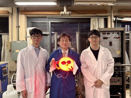
< Figure 1. Overall concept of face-fit surface-lighting micro-LEDs (FSLED) mask. a. Optical image of the FSLED mask showing uniform surface-lighting. schematic illustration of the FSLED mask. The 2D to 3D transformation procedure b. Difference in cosmetic effect on deep skin elasticity, wrinkles, and sagging between FSLED mask and CLED mask. (improvement percentage in eight weeks) >
Conventional LED masks, with their rigid design, fail to conform closely to the skin's contours. This limitation causes substantial light reflection, with up to 90% reflected over a distance of 2 cm, reducing light penetration and limiting stimulation of the deep skin layers essential for effective skin rejuvenation.
To address these challenges, Professor Lee's team developed a face-conforming surface lighting micro-LED (FSLED) mask, which can provide uniform photostimulation to the dermis. The key technology lies in the mask's ability to deliver uniform light to deep skin tissues while maintaining a conformal skin attachment. This is achieved through a 3D origami structure, integrated with 3,770 micro-LEDs and flexible surface light-diffusion layer, minimizing the gaps between the light source and the skin.
In clinical trials involving 33 participants, the FSLED mask demonstrated a 340% improvement in deep skin elasticity compared to conventional LED masks, proving its efficacy in significantly reducing skin wrinkles, sagging and aging.
Professor Keon Jae Lee said, “The FSLED mask provides cosmetic benefits to the entire facial dermis without the side effects of low-temperature burns, making home-care anti-aging treatment that enhances the quality of human life possible. The product is being manufactured by Fronics, KAIST startup company, and will be distributed globally through Amorepacific's network, with sales starting in November.”
This result titled “Clinical Validation of Face-fit Surface-lighting Micro Light-emitting Diode Mask for Skin Anti-aging Treatment”, in which Min Seo Kim, a student of the Master-Doctorate integrated program, and Jaehun An, a Ph.D. candidate, in the Department of Materials Science and Engineering of KAIST, took part as co-first authors, was published in Advanced Materials on October 22nd, 2024 (DOI: 10.1002/adma.202411651).
Introductory Video: Face-conforming surface LED mask for skin anti-aging ( https://www.youtube.com/watch?v=kSccLwx8N_w )
2024.10.29 View 5608
 -
 A KAIST Team Develops Selective Transfer Printing Technology for MicroLEDs
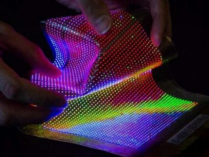
- A KAIST research team led by Professor Keon Jae Lee demonstrates the transfer printing of a large number of micro-sized inorganic semiconductor chips via the selective modulation of micro-vacuum force.
MicroLEDs are a light source for next-generation displays that utilize inorganic LED chips with a size of less than 100 μm. MicroLEDs have attracted a great deal of attention due to their superior electrical/optical properties, reliability, and stability compared to conventional displays such as LCD, OLED, and QD. To commercialize microLEDs, transfer printing technology is essential for rearranging microLED dies from a growth substrate onto the final substrate with a desired layout and precise alignment. However, previous transfer methods still have many challenges such as the need for additional adhesives, misalignment, low transfer yield, and chip damage.
Professor Lee’s research team has developed a micro-vacuum assisted selective transfer printing (µVAST) technology to transfer a large number of microLED chips by adjusting the micro-vacuum suction force.
The key technology relies on a laser-induced etching (LIE) method for forming 20 μm-sized micro-hole arrays with a high aspect ratio on glass substrates at fabrication speed of up to 7,000 holes per second. The LIE-drilled glass is connected to the vacuum channels, controlling the micro-vacuum force at desired hole arrays to selectively pick up and release the microLEDs. The micro-vacuum assisted transfer printing accomplishes a higher adhesion switchability compared to previous transfer methods, enabling the assembly of micro-sized semiconductors with various heterogeneous materials, sizes, shapes, and thicknesses onto arbitrary substrates with high transfer yields.
< Figure 01. Concept of micro-vacuum assisted selective transfer printing (μVAST). >
Professor Keon Jae Lee said, “The micro-vacuum assisted transfer provides an interesting tool for large-scale, selective integration of microscale high-performance inorganic semiconductors. Currently, we are investigating the transfer printing of commercial microLED chips with an ejector system for commercializing next-generation displays (Large screen TVs, flexible/stretchable devices) and wearable phototherapy patches.”
This result titled “Universal selective transfer printing via micro-vacuum force” was published in Nature Communications on November 26th, 2023. (DOI: 10.1038/S41467-023-43342-8)
< Figure 02. Universal transfer printing of thin-film semiconductors via μVAST. >
< Figure 03. Flexible devices fabricated by μVAST. >
Title: Entire process including LIE and µVAST
Vimeo link: https://vimeo.com/894430416?share=copy
2023.12.19 View 4143
 -
 KAIST Team Develops Highly-Sensitive Wearable Piezoelectric Blood Pressure Sensor for Continuous Health Monitoring
- A collaborative research team led by KAIST Professor Keon Jae Lee verifies the accuracy of the highly-sensitive sensor through clinical trials
- Commercialization of the watch and patch-type sensor is in progress
A KAIST research team led by Professor Keon Jae Lee from the Department of Materials Science and Engineering and the College of Medicine of the Catholic University of Korea has developed a highly sensitive, wearable piezoelectric blood pressure sensor.
Blood pressure is a critical indicator for assessing general health and predicting stroke or heart failure. In particular, cardiovascular disease is the leading cause of global death, therefore, periodic measurement of blood pressure is crucial for personal healthcare.
Recently, there has been a growing interest in healthcare devices for continuous blood pressure monitoring. Although smart watches using LED-based photoplethysmography (PPG) technology have been on market, these devices have been limited by the accuracy constraints of optical sensors, making it hard to meet the international standards of automatic sphygmomanometers.
Professor Lee’s team has developed the wearable piezoelectric blood pressure sensor by transferring a highly sensitive, inorganic piezoelectric membrane from bulk sapphire substrates to flexible substrates. Ultrathin piezoelectric sensors with a thickness of several micrometers (one hundredth of the human hair) exhibit conformal contact with the skin to successfully collect accurate blood pressure from the subtle pulsation of the blood vessels.
Clinical trial at the St. Mary’s Hospital of the Catholic University validated the accuracy of blood pressure sensor at par with international standard with errors within ±5 mmHg and a standard deviation under 8 mmHg for both systolic and diastolic blood pressure. In addition, the research team successfully embedded the sensor on a watch-type product to enable continuous monitoring of blood pressure.
Prof. Keon Jae Lee said, “Major target of our healthcare devices is hypertensive patients for their daily medical check-up. We plan to develop a comfortable patch-type sensor to monitor blood pressure during sleep and have a start-up company commercialize these watch and patch-type products soon.”
This result titled “Clinical validation of wearable piezoelectric blood pressure sensor for health monitoring” was published in the online issue of Advanced Materials on March 24th, 2023. (DOI: 10.1002/adma.202301627)
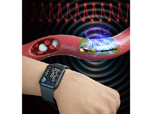
Figure 1. Schematic illustration of the overall concept for a wearable piezoelectric blood pressure sensor (WPBPS).
Figure 2. Wearable piezoelectric blood pressure sensor (WPBPS) mounted on a watch (a) Schematic design of the WPBPS-embedded wristwatch. (b) Block diagram of the wireless communication circuit, which filters, amplifies, and transmits wireless data to portable devices. (c) Pulse waveforms transmitted from the wristwatch to the portable device by the wireless communication circuit. The inset shows a photograph of monitoring a user’s beat-to-beat pulses and their corresponding BP values in real time using the developed WPBPS-mounted wristwatch.
2023.04.17 View 8217