FET
-
 KAIST to Collaborate with AT&C to Take Dominance over Dementia
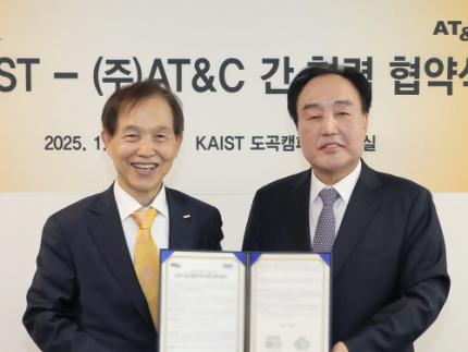
< Photo 1. (From left) KAIST Dean of the College of Natural Sciences Daesoo Kim, KAIST President Kwang Hyung Lee, AT&C Chairman Ki Tae Lee, AT&C CEO Jong-won Lee >
KAIST (President Kwang Hyung Lee) announced on January 9th that it signed a memorandum of understanding for a comprehensive mutual cooperation with AT&C (CEO Jong-won Lee) at its Seoul Dogok Campus to expand research investment and industry-academia cooperation in preparation for the future cutting-edge digital bio era.
Senile dementia is a rapidly increasing brain disease that affects 10% of the elderly population aged 65 and older, and approximately 38% of those aged 85 and older suffer from dementia. Alzheimer's disease is the most common dementia in the elderly and its prevalence has been increasing rapidly in the population of over 40 years of age. However, an effective treatment is yet to be found.
The Korean government is investing a total of KRW 1.1 trillion in dementia R&D projects from 2020 to 2029, with the goal of reducing the rate of increase of dementia patients by 50%. Since it takes a lot of time and money to develop effective and affordable medicinal dementia treatments, it is urgent to work on the development of digital treatments for dementia that can be applied more quickly.
AT&C, a digital healthcare company, has already received approval from the Ministry of Food and Drug Safety (MFDS) for its device for antidepressant treatment based on transcranial magnetic stimulation (TMS) using magnetic fields and is selling it domestically and internationally. In addition, it has developed the first Alzheimer's dementia treatment device in Korea and received MFDS approval for clinical trials. After passing phase 1 to evaluate safety and phase 2 to test efficacy on some patients, it is currently conducting phase 3 clinical trials to test efficacy on a larger group of patients.
This dementia treatment device is equipped with a system that combines non-invasive electronic stimulations (TMS electromagnetic stimulator) and digital therapeutic prescription (cognitive learning programs) to provide precise, automated treatment by applying AI image analysis and robotics technology.
Through this agreement, KAIST and AT&C have agreed to cooperate with each other in the development of innovative digital treatment equipment for brain diseases. Through research collaboration with KAIST, AT&C will be able to develop technology that can be widely applied to Parkinson's disease, stroke, mild cognitive impairment, sleep disorders, etc., and will develop portable equipment that can improve brain function and prevent dementia at home by utilizing KAIST's wearable technology.
To this end, AT&C plans to establish a digital healthcare research center at KAIST by supporting research personnel and research expenses worth approximately 3 billion won with the goal of developing cutting-edge digital equipment within 3 years.
The digital equipment market is expected to grow at a compounded annual growth rate of 22.1% from 2023 to 2033, reaching a market size of $1.9209 trillion by 2033.
< Photo 2. (From left) Dean of the KAIST College of Natural Sciences Daesoo Kim, Professor Young-joon Lee, Professor Minee Choi of the KAIST Department of Brain and Cognitive Sciences, KAIST President Kwang Hyung Lee, Chairman Ki Tae Lee, CEO Jong-won Lee, and Headquarters Director Ki-yong Na of AT&C >
CEO Jong-won Lee said, “AT&C is playing a leading role in the treatment of Alzheimer’s disease using TMS (transcranial magnetic stimulation) technology. Through this agreement with KAIST, we will do our best to create a new paradigm for brain disease treatment and become a platform company that can lead future medical devices and medical technology.”
Former Samsung Electronics Vice Chairman Ki Tae Lee, a strong supporter of this R&D project, said, “Through this agreement with KAIST, we plan to prepare for a new future by combining the technologies AT&C has developed so far with KAIST’s innovative and differentiated technologies.”
KAIST President Kwang Hyung Lee emphasized, “Through this collaboration, KAIST expects to build a world-class digital therapeutics infrastructure for treating brain diseases and contribute greatly to further strengthening Korea’s competitiveness in the biomedical field.”
The signing ceremony was attended by KAIST President Kwang Hyung Lee, the Dean of KAIST College of Natural Sciences Daesoo Kim, AT&C CEO Lee Jong-won, and the current Chairman of AT&C, Ki Tae Lee, former Vice Chairman of Samsung Electronics.
2025.01.09 View 4787
 -
 Black Phosphorous Tunnel Field-Effect Transistor as an Alternative Ultra-low Power Switch
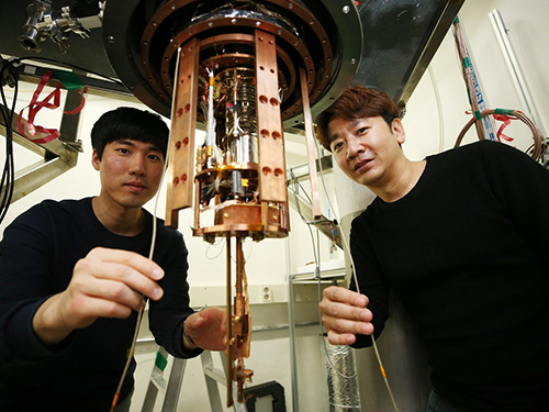
Researchers have reported a black phosphorus transistor that can be used as an alternative ultra-low power switch. A research team led by Professor Sungjae Cho in the KAIST Department of Physics developed a thickness-controlled black phosphorous tunnel field-effect transistor (TFET) that shows 10-times lower switching power consumption as well as 10,000-times lower standby power consumption than conventional complementary metal-oxide-semiconductor (CMOS) transistors.
The research team said they developed fast and low-power transistors that can replace conventional CMOS transistors. In particular, they solved problems that have degraded TFET operation speed and performance, paving the way to extend Moore’s Law.
In the study featured in Nature Nanotechnology last month, Professor Cho’s team reported a natural heterojunction TFET with spatially varying layer thickness in black phosphorous without interface problems. They achieved record-low average subthreshold swing values over 4-5 dec of current and record-high, on-state current, which allows the TFETs to operate as fast as conventional CMOS transistors with as much lower power consumption.
"We successfully developed the first transistor that achieved the essential criteria for fast, low-power switching. Our newly developed TFETs can replace CMOS transistors by solving a major issue regarding the performance degradation of TFETs,"Professor Cho said.
The continuous down-scaling of transistors has been the key to the successful development of current information technology. However, with Moore’s Law reaching its limits due to the increased power consumption, the development of new alternative transistor designs has emerged as an urgent need.
Reducing both switching and standby power consumption while further scaling transistors requires overcoming the thermionic limit of subthreshold swing, which is defined as the required voltage per ten-fold current increase in the subthreshold region. In order to reduce both the switching and standby power of CMOS circuits, it is critical to reduce the subthreshold swing of the transistors.
However, there is fundamental subthreshold swing limit of 60 mV/dec in CMOS transistors, which originates from thermal carrier injection. The International Roadmap for Devices and Systems has already predicted that new device geometries with new materials beyond CMOS will be required to address transistor scaling challenges in the near future. In particular, TFETs have been suggested as a major alternative to CMOS transistors, since the subthreshold swing in TFETs can be substantially reduced below the thermionic limit of 60 mV/dec. TFETs operate via quantum tunneling, which does not limit subthreshold swing as in thermal injection of CMOS transistors.
In particular, heterojunction TFETs hold significant promise for delivering both low subthreshold swing and high on-state current. High on-current is essential for the fast operation of transistors since charging a device to on state takes a longer time with lower currents. Unlike theoretical expectations, previously developed heterojunction TFETs show 100-100,000x lower on-state current (100-100,000x slower operation speeds) than CMOS transistors due to interface problems in the heterojunction. This low operation speed impedes the replacement of CMOS transistors with low-power TFETs.
Professor Cho said, “We have demonstrated for the first time, to the best of our knowledge, TFET optimization for both fast and ultra-low-power operations, which is essential to replace CMOS transistors for low-power applications.” He said he is very delighted to extend Moore’s Law, which may eventually affect almost every aspect of life and society. This study (https://doi.org/10.1038/s41565-019-0623-7) was supported by the National Research Foundation of Korea.
Publication:
Kim et al. (2020) Thickness-controlled black phosphorus tunnel field-effect transistor for low-power switches. Nature Nanotechnology. Available online at https://doi.org/10.1038/s41565-019-0623-7
Profile:
Professor Sungjae Cho
sungjae.cho@kaist.ac.kr
Department of Physics
http://qtak.kaist.ac.kr/
KAIST
Profile:
Seungho Kim, PhD Candidate
krksh21@kaist.ac.kr
Department of Physics
http://qtak.kaist.ac.kr/
KAIST
(END)
2020.02.21 View 13505
 -
 KAIST International Community Celebrates the Year-End
KAIST international community all gathered in celebration of the year-end on December 5 at the KAIST auditorium. This year, the community made the year-end party very special, expressing their appreciation very touching way at the event hosted by the International Scholar and Student Services (ISSS). Nearly 650 international faculty, students, and their family members joined the party.
Currently, 184 faculty members and researchers from 29 countries are working at KAIST, with 901 international students from 92 countries enrolled.
The two-hour party offered them a chance to enjoy a wide variety of activities and events, including dance performances, student performances, games, and dinner.
The party also had a meaningful award ceremony. Prior to the event, a month-long survey was conducted, asking international scholars and students which on-campus team they were most thankful for this year. Candidates for the appreciation award were: Safety and Security Team, Student Affairs Team, Campus Police, dormitory supervisors, and campus cleaning staff.
Approximately 470 scholars and students responded to the survey and 214 voted for the campus cleaning staff (45.5%).
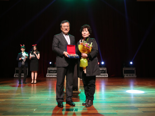
(President Sung-Chul Shin and Myeongja Kim)
Ms. Myeongja Kim, a director of the cleaning staff in the undergraduate zone, received the award on behalf of the entire cleaning staff. At the ceremony, President Sung-Chul Shin conferred the award.
President Shin in his welcoming remarks said that globalization is his priority and urgent mission. To make KAIST more globalized, he said he will focus on three agendas; to make the campus KAIST a more welcoming environment for international community; to make campus more inclusive and diverse; to enhance the global visibility of KAIST more proactively. Click for the full text of opening remarks
2017.12.11 View 6606
 -
 Professor Poong Hyun Seong Selected as Fellow of the ANS
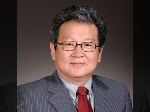
Professor Poong Hyun Seong of the Department of Nuclear and Quantum Engineering was selected as a fellow of the American Nuclear Society.
The selection was announced at their annual meeting held in San Francisco on June 12, in recognition of Professor Seong's contributions to the field of nuclear instrumentation, control andhuman factors engineering.
Founded in 1954, the American Nuclear Society selects scholars who have made outstanding achievements and contributions to the development of the nuclear engineering field each year.
Professor Seong's researches in the field of nuclear instrumentation, control and human factors engineering have contributed to the safe operation of nuclear power plants, to the development of systems to maintain nuclear power plants safely in the event of emergency and to the enhancement of effective response capabilities of nuclear power plant operators. His researches significantly contributed to the safety improvement of nuclear power plants and have been recognized worldwide.
Professor Seong said, "Korea has emerged as a nuclear powerhouse. I think not only my academic career but our national reputation in the field of nuclear research has been well recognized by our global peers.” Professor Seong has served as president of the Korean Nuclear Society, editor in chief of Nuclear Engineering and Technology, and as a commissioner of the Korean Nuclear Safety Commission. He is currently working as a commissioner of the Korean Atomic Energy Commission.
2017.06.29 View 8944
 -
 KATT Tops at Appropriate Technology Competition
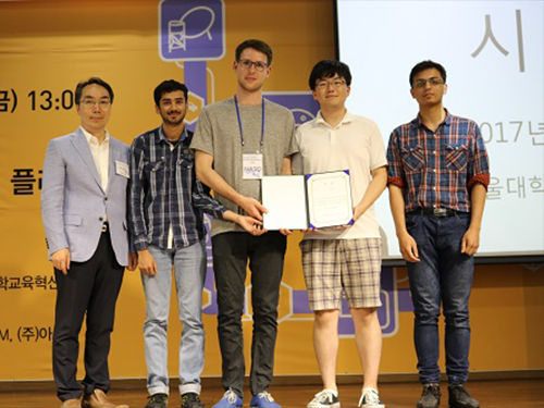
The KAIST Appropriate Technology Team (KATT) consisting of KAIST international students received gold and bronze awards at ‘the 9th Creative Design Competition for the Other 90%’. This year’s competition was hosted by the Ministry of Science, ICT and Future Planning at Seoul National University’s Global Convention Plaza on May 26. Undergraduate and graduate students nationwide formed 65 teams to participate in the competition.
The aim of the competition is to discover appropriate technology and sustainable design items to enhance quality of life for those with no or little access to science technology and its products around the world. This year’s competition categorized the designs into IT; water and energy; agriculture, hygiene, safety, and housing; and education. The teams were evaluated on their presentations and prototypes.
KATT produced alarm warning bracelets for people in developing countries and smart hybrid dryers for agricultural products. The alarm warning bracelets were designed for those living in tsunami risk zones; they use wireless communication technology to receive and transmit warning signals and can be produced for less than $4.
The smart hybrid dryers featured solar energy generation, aimed to help those with low income in subtropical, low-altitude regions with unstable climates, since there are currently no drying methods for agricultural products without direct exposure to sunlight. Therefore, the hybrid dryers allowed drying regardless of the weather, and thus increased the storage and distribution efficiency of agricultural products.
Ashar Alam from India who participated in developing the alarm warning bracelet said, “Through the appropriate technology club, I recognized problems in India that also affect neighboring countries such as Indonesia and Bangladesh. I wanted to actively use the science and technology knowledge I have accumulated in KAIST for the less fortunate.” He continued, “It was meaningful to develop the product using the respective talents of students from various countries with the spirit of developing appropriate technology.”
(Photo caption: Alarm warning bracelet team received the gold award)
2017.06.12 View 8995
 -
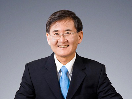 President Steve Kang Receives the John Choma Education Award from the IEEE International Symposium on Circuits and Systems
The Institute of Electrical and Electronics Engineers (IEEE) International Symposium on Circuits and Systems (ISCAS) 2015 took place at the Cultural Centre of Belem in Lisbon, Portugal, on May 24-27, 2015.
President Steve Kang attended the conference and presented a paper entitled “Memrister-based Synapses and Neurons for Neuromorphic Computing” on May 26, 2015. On the same day, he received the John Choma Education Award.
The award was established to commemorate the lifetime achievement of the late Professor John Choma of the Electrical Engineering Department at the University of Southern California. Dr. Choma was an eminent scientist, scholar, and educator, who earned global recognition in the field of integrated circuits and very-large-scale-integration (VLSI).
The IEEE ISCAS selects, among its members, the recipient of the John Choma Education Award, who has made significant contributions to the education of circuits and systems.
President Kang advised 60 doctorates while teaching at the University of Illinois at Urbana-Champaign and the University of California at Santa Cruz and published 450 research papers in the past 40 years. He also received Meritorious Service Award, Charles Desoer Technical Achievement Award, and Mac Van Valkenburg Society Award, all from the IEEE ISCAS.
2015.06.03 View 7977
 -
 KAIST Develops Ultrathin Polymer Insulators Key to Low-Power Soft Electronics
Using an initiated chemical vapor deposition technique, the research team created an ultrathin polymeric insulating layer essential in realizing transistors with flexibility and low power consumption. This advance is expected to accelerate the commercialization of wearable and soft electronics.
A group of researchers at the Korea Advanced Institute of Science and Technology (KAIST) developed a high-performance ultrathin polymeric insulator for field-effect transistors (FETs). The researchers used vaporized monomers to form polymeric films grown conformally on various surfaces including plastics to produce a versatile insulator that meets a wide range of requirements for next-generation electronic devices. Their research results were published online in Nature Materials on March 9th, 2015.
FETs are an essential component for any modern electronic device used in our daily life from cell phones and computers, to flat-panel displays. Along with three electrodes (gate, source, and drain), FETs consist of an insulating layer and a semiconductor channel layer. The insulator in FETs plays an important role in controlling the conductance of the semiconductor channel and thus current flow within the translators. For reliable and low-power operation of FETs, electrically robust, ultrathin insulators are essential. Conventionally, such insulators are made of inorganic materials (e.g., oxides and nitrides) built on a hard surface such as silicon or glass due to their excellent insulating performance and reliability.
However, these insulators were difficult to implement into soft electronics due to their rigidity and high process temperature. In recent years, many researchers have studied polymers as promising insulating materials that are compatible with soft unconventional substrates and emerging semiconductor materials. The traditional technique employed in developing a polymer insulator, however, had the limitations of low surface coverage at ultra-low thickness, hindering FETs adopting polymeric insulators from operating at low voltage.
A KAIST research team led by Professor Sung Gap Im of the Chemical and Biomolecular Engineering Department and Professor Seunghyup Yoo and Professor Byung Jin Cho of the Electrical Engineering Department developed an insulating layer of organic polymers, “pV3D3,” that can be greatly scaled down, without losing its ideal insulating properties, to a thickness of less than 10 nanometers (nm) using the all-dry vapor-phase technique called the “initiated chemical vapor deposition (iCVD).”
The iCVD process allows gaseous monomers and initiators to react with each other in a low vacuum condition, and as a result, conformal polymeric films with excellent insulating properties are deposited on a substrate. Unlike the traditional technique, the surface-growing character of iCVD can overcome the problems associated with surface tension and produce highly uniform and pure ultrathin polymeric films over a large area with virtually no surface or substrate limitations. Furthermore, most iCVD polymers are created at room temperature, which lessens the strain exerted upon and damage done to the substrates.
With the pV3D3 insulator, the research team built low-power, high-performance FETs based on various semiconductor materials such as organics, graphene, and oxides, demonstrating the pV3D3 insulator’s wide range of material compatibility. They also manufactured a stick-on, removable electronic component using conventional packaging tape as a substrate. In collaboration with Professor Yong-Young Noh from Dongguk University in Korea, the team successfully developed a transistor array on a large-scale flexible substrate with the pV3D3 insulator.
Professor Im said, “The down-scalability and wide range of compatibility observed with iCVD-grown pV3D3 are unprecedented for polymeric insulators. Our iCVD pV3D3 polymeric films showed an insulating performance comparable to that of inorganic insulating layers, even when their thickness were scaled down to sub-10 nm. We expect our development will greatly benefit flexible or soft electronics, which will play a key role in the success of emerging electronic devices such as wearable computers.”
The title of the research paper is “Synthesis of ultrathin polymer insulating layers by initiated chemical vapor deposition for low-power soft electronics” (Digital Object Identifier (DOI) number is 10.1038/nmat4237).
Picture 1: A schematic image to show how the initiated chemical vapor deposition (iCVD) technique produces pV3D3 polymeric films: (i) introduction of vaporized monomers and initiators, (ii) activation of initiators to thermally dissociate into radicals, (iii) adsorption of monomers and initiator radicals onto a substrate, and (iv) transformation of free-radical polymerization into pV3D3 thin films.
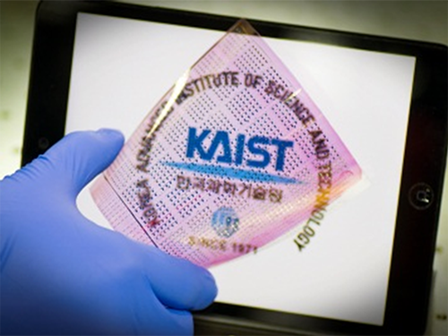
Picture 2: This is a transistor array fabricated on a large scale, highly flexible substrate with pV3D3 polymeric films.
Picture 3: This photograph shows an electronic component fabricated on a conventional packaging tape, which is attachable or detachable, with pV3D3 polymeric films embedded.
2015.03.10 View 14410
 -
 KAIST Conducts Safety Awareness Campaign for Research and Experiment
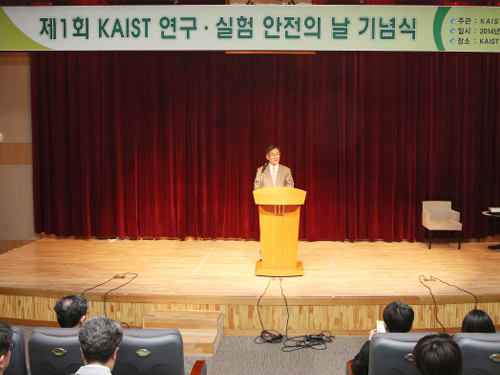
KAIST had an opening ceremony to hold its first “Safety Awareness Campaign for Research and Experiment” on 13th May. Over 100 people attended the ceremony, including President Steve Kang, Provost Gyu-Ho Park, and the Dean of the Administration Office Jae-Nam Lee, as well as the Chief of the Department of Research Environment Safety from the Ministry of Science, ICT and Future Planning, Republic of Korea.
On the day of the event, Year 2014 was proclaimed as the first year of accident-free KAIST research and laboratory facilities.
A certificate of merit was awarded to promote safe and comfortable research environments. The Department of Civil and Environmental Engineering, KAIST, was selected as the department with the best lab safety management and the Department of Mechanical Engineering as the second.
Along with the merit award ceremony, the results of the “7th Research and Laboratory Safety Campaign Contest” were announced: “Lady First When Dating, Safety First When Experimenting!” written by Jong-Su Bae from the Department of Mechanical Engineering was selected as the best slogan, and Hyeon-Chae Noh from the Department of Civil and Environmental Engineering received the award for best poster.
President Steve Kang said, “KAIST is constantly striving to establish a comprehensive safety management system and to promote a safe research and laboratory environment,” and “To ensure the safety of KAIST and its members, we will be as supportive as possible.”
Below is the winner of the poster from the 7th Research and Laboratory Safety Campaign Contest.
What Would You Rather Wear? Gloves or Bandages?
Gloves worn in laboratories are protection from hazardous materials that students and researchers may come in contact with. The poster emphasizes the importance of wearing protective gloves when conducting research or experiment.
2014.05.19 View 9033
 -
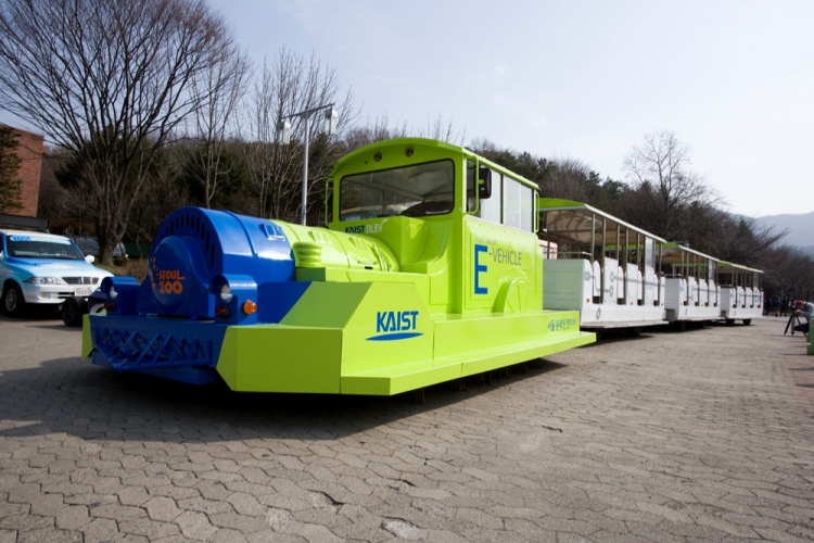 OLEV Safety Confirmed by International Standards
On September 19, KAIST announced that the electromagnetic (EM) field levels of its online electric vehicle (OLEV) measured in June and September of this year demonstrated verification of its safety.
Last June, the EM field level of OLEV installed at the Seoul Grand Park was measured by the Korea Research Institute of Standards and Science (KRISS) to test its harmfulness to human. The results were 0.5 ~ 61mG which is within the national and international standards of 62.5mG.
KRISS measured EM field levels on 22 spots on the side of and at the center of OLEV at a fixed distance (30cm) but variable heights (5cm~150cm) according to the national standard of measurement methods for electromagnetic fields of household appliances and similar apparatuses with regard to human exposure (IEC 62233).
In addition, another testing took place on September 13 following a request by National Assemblywoman Young-Ah Park, a member of the National Assembly’s Education, Science and Technology Committee, who has raised an issue on the safety of OLEV. This testing session was held by EMF Safety, Inc., an institution designated by Park, and it tested the EM field level of the same OLEV train that was tested in June.
As a result, the September measurements were well within the national and international standards with 0~24.1mG. The test was conducted under the presence of third party to produce a fair and objective result.
As reference, the EM field level results are well within the American IEEE electromagnetic field standards of 1,100 mG.
The September measurements were produced by Park’s recommendation of following the criteria specified in the measurement procedures of IEC 62110, “Electric and magnetic field levels generated by AC power systems to public exposure,” which were 15 measurements at a fixed 20cm distance at the side of and from the center of OLEV with variable heights of 50cm~150cm.
2010.09.27 View 14404
 -
 Prof. Seong Publishes English Book on Reliability in Digital Control Systems
Prof. Poong-Hyun Seong of Department of Nuclear and Quantum Engineering has recently published an English-language book on reliability and risk issues in large scale safety-critical digital control systems used in complex facilities such as nuclear power plants.
The book entitled “Reliability and Risk Issues in Large Scale Safety-critical Digital Control Systems” is a result of Prof. Seong’s collaboration with some KAIST graduates who used to be under his guidance. The 303-page publication has been published by Springer, one of the world’s leading publishers of academic journals, as part of the Springer Series in Reliability Engineering.
The book consists of four parts; part I deals with issues related to hardware, part II software, part III human factors and finally the last part integrated systems. It can be purchased through some on-line book stores such as Amazon.com.
Prof. Seong served as an editor-in-chief for Nuclear Engineering and Technology (NET), an international journal of Korean Nuclear Society (KNS), from 2003 to 2008. He also worked as a chair of the Human Factors Division (HFD) of American Nuclear Society (ANS) from 2006 to 2007. Prof. Seong is now a commissioner of Korea Nuclear Safety Commission which is the nation’s highest committee on Nuclear Safety.
2008.12.26 View 19209
 -
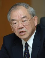 President Nam-Pyo Suh Receives Lifetime Achievement Award from SPE
President Nam-Pyo Suh has been selected as a recipient of the Lifetime Achievement Award by the Society of Plastic Engineers (SPE).
The SPE is the largest professional organization that promotes polymer-related R&D.
The SPE announced that it recognizes President Suh’s many contributions to the field of polymer processing. President Suh established the first university/industry cooperative research program at MIT known as the MIT-Industry Polymer Processing Program, which became a model in establishing similar programs at many other universities by NSF. Among the many new materials, products and manufacturing processes invented by him are: Microcellular plastics, known as MuCell and used commercially worldwide, USM high pressure foam molding technology, electrostatic charge-decay NDE technique for polymeric materials, and foam/straight plastic lamination process (a major industrial product).
2007.04.12 View 15848