Nano
-
 Firefly inspired high efficiency LED technology developed
A firefly inspired, high efficiency self-illuminating LED has been developed.
Professor Jeong Gi Hoon (Department of Bio and Brain Engineering) mimicked the nanostructure of the external layer of the illumination organ of a firefly and succeeded in fabricating high illumination efficiency LED lenses.
Conventional lenses required expensive anti-reflection coating. The developed lenses utilize the bio-inspired nanostructure on the surface of the lenses themselves to reduce the reflectivity of the lenses thereby decreasing production costs.
The developed antireflection nanostructure is expected to be applied to various digital devices and lighting fixtures.
Antireflective structures have been applied in various fields in order to enhance light efficiency However these structures have been limited to flat surfaces and therefore was difficult to implement to curved surfaces like LED lenses.
Professor Jeong’s team solved this problem by using three dimensional micro molding processes.
The team fabricated the nanostructure by forming a single nanoparticle layer on the silicon oxide and performing dry etching. On this nanostructure PDMS was poured and manipulated to fabricate a lens structure similar to that of a firefly.
The fabricated lens showed similar efficiency as conventional antireflection coating.
2012.11.29 View 7196
Firefly inspired high efficiency LED technology developed
A firefly inspired, high efficiency self-illuminating LED has been developed.
Professor Jeong Gi Hoon (Department of Bio and Brain Engineering) mimicked the nanostructure of the external layer of the illumination organ of a firefly and succeeded in fabricating high illumination efficiency LED lenses.
Conventional lenses required expensive anti-reflection coating. The developed lenses utilize the bio-inspired nanostructure on the surface of the lenses themselves to reduce the reflectivity of the lenses thereby decreasing production costs.
The developed antireflection nanostructure is expected to be applied to various digital devices and lighting fixtures.
Antireflective structures have been applied in various fields in order to enhance light efficiency However these structures have been limited to flat surfaces and therefore was difficult to implement to curved surfaces like LED lenses.
Professor Jeong’s team solved this problem by using three dimensional micro molding processes.
The team fabricated the nanostructure by forming a single nanoparticle layer on the silicon oxide and performing dry etching. On this nanostructure PDMS was poured and manipulated to fabricate a lens structure similar to that of a firefly.
The fabricated lens showed similar efficiency as conventional antireflection coating.
2012.11.29 View 7196 -
Principle behind increasing the catalytic property of nanocatalysts proven
The technology that allows full control of the catalytic property of nanocatalysts using oxide formation on nanocatalysts has been developed by KAIST researchers. The breakthrough opens up the possibility of the development of a new kind of catalysts that maximizes catalytic property and minimizes waste.
*nanocatalyst is a material that catalyzes gas reactions on its surface. It is composed of a high surface area oxide scaffold with nano-sized metal particles dispersed.
The team was led by Professor Park Jeong Young of the KAIST EEWS Graduate School and consists of Kamran Qadir Ph.D. candidate (1st Author), Professor Joo Sang Hoon of UNIST, Professor Moon Bong Jin of Hanyang University, and Professor Gabor Somorajai of UC Berkeley. Support for the research was provided from Ministry of Education Science and Technology, National Research Foundation, and Ministry of Knowledge Economy. The results were published as the online edition of Nano Letters: “Intrinsic Relation between Catalytic Activity of CO Oxidation on Ru Nanoparticles and Ru Oxides Uncovered with Ambient Pressure XPS”.
Catalysts are included in above 80% of all the products used in everyday life and are therefore included in most aspects of our lives.
The focus on nanocatalysts is based on finding solutions to increasing the efficiency for application to energy production and for solving environmental issues.
Most nanocatalysts are composed of nanoparticles and oxides where the nanoparticles increase the surface area of the catalyst to increase its activity.
The efficiency of a nanocatalyst is affected by the surface oxide of the nanoparticles. However the proving of this assumption remained difficult to do as it required in-situ measurement of the oxide state of the nanoparticles in the specific environment. Thus far, the experiments were conducted in a vacuum and therefore did not reflect the actual behavior in real life. The recently developed X-ray Photoelectron Spectroscopy allows for measurement of the oxidization state at standard atmospheric pressure.
Professor Park’s research team successfully measured the oxidization state of the nanoparticle using the atmospheric pressure X-ray Photoelectron Spectroscopy in the specified environment.
They confirmed the effect the oxidization state on the catalytic effect of the nanoparticles and additionally found that a thin layer of oxide can increase the catalytic effect and the effectiveness of the nanoparticle can controlled by the oxidation state.
2012.11.29 View 7636
-
Professor Yoon Dong Ki becomes first Korean to Receive the Michi Nakata Prize
Professor Yoon Dong Ki (Graduate School of Nano Science and Technology) became the first Korean to receive the Michi Nakata Prize from the International Liquid Crystal Society.
The Awards Ceremony was held on the 23rd of August in Mainz, Germany in the 24th Annual International Liquid Crystal Conference.
The Michi Nakata Prize was initiated in 2008 and is rewarded every two years to a young scientist that made a ground breaking discovery or experimental result in the field of liquid crystal. Professor Yoon is the first Korean recipient of the Michi Nakata Prize.
Professor Yoon is the founder of the patterning field that utilizes the defect structure formed by smectic displays. He succeeded in large scale patterning complex chiral nano structures that make up bent-core molecules.
Professor Yoon’s experimental accomplishment was published in the Advanced Materials magazine and the Proc. Natl. Acad. Sci. U.S.A. and also as the cover dissertation of Liquid Crystals magazine.
Professor Yoon is currently working on Three Dimensional Nano Patterning of Supermolecular Liquid Crystal and is part of the World Class University organization.
2012.09.11 View 9757
-
Ultra Elastic Electrode Material Developed
KAIST research team succeeded in developing the next generation flexible and elastic electrode material crucial in the development of flexible displays, wearable computers, and etc.
Professor Jeon Seok Woo’s team of the department of Materials Science and Engineering succeeded in the development of a super elastic material.
The result of the experiment was introduced as the research highlight in Nature Communications and is especially significant as the main driving force behind the achievement were domestic researchers.
Professor Jeons team developed a structured three dimensional nano-porous structure over a 1inch by 1inch area that is 10micrometers in thickness. The structure is fabricated using world’s largest area three dimensional nano patterning technique.
The nano-porous structure was injected with elastomeric material and was subsequently removed to yield an inverse three dimensional elastic nano material. The pores were infiltrated with liquid conductive material which yielded a super elastic flexible electrode.
The fabricated electrode showed amazing elasticity levels and was able to light LED lamps in a 200% stretched state without decrease in electrical conductivity.
Conventional methods included folding and expanding a material like an accordion or creating a mesh-like structure by making holes in the material. However these methods yielded materials with limited elasticity and even 100% stretching resulted in the drastic decrease in electrical conductivity.
Professor Jeon expects the domestically developed technology to obtain the upper hand in the market and make great contributions in both science and society.
2012.07.26 View 8346
-
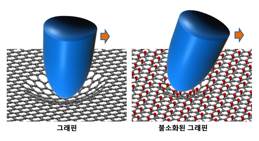 KAIST researchers verify and control the mechanical properties of graphene
KAIST researchers have successfully verified and controlled the mechanical properties of graphene, a next-generation material. Professor Park Jung Yong from the EEWS Graduate School and Professor Kim Yong Hyun from the Graduate School of Nanoscience and Technology have succeeded in fluorinating a single atomic-layered graphene sample and controlling its frictional and adhesive properties. This is the first time the frictional properties of graphene have been examined at the atomic level, and the technology is expected to be applied to nano-sized robots and microscopic joints.
Graphene is often dubbed “the dream material” because of its ability to conduct high amounts of electricity even when bent, making it the next-generation substitute for silicon semiconductors, paving the way for flexible display and wearable computer technologies. Graphene also has high potential applications in mechanical engineering because of its great material strength, but its mechanical properties remained elusive until now.
Professor Park’s research team successfully produced individual graphene samples with fluorine-deficiency at the atomic level by placing the samples in Fluoro-xenon (XeF2) gas and applying heat. The surface of the graphene was scanned using a micro probe and a high vacuum atomic microscope to measure its dynamic properties.
The research team found that the fluorinated graphene sample had 6 times more friction and 0.7 times more adhesiveness than the original graphene. Electrical measurements confirmed the fluorination process, and the analysis of the findings helped setup the theory of frictional changes in graphene.
Professor Park stated that “graphene can be used for the lubrication of joints in nano-sized devices” and that this research has numerous applications such as the coating of graphene-based microdynamic devices.
This research was published in the online June edition of Nano Letters and was supported by the Ministry of Science, Technology, and Education and the National Research Foundation as part of the World Class University (WCU) program.
2012.07.24 View 12180
KAIST researchers verify and control the mechanical properties of graphene
KAIST researchers have successfully verified and controlled the mechanical properties of graphene, a next-generation material. Professor Park Jung Yong from the EEWS Graduate School and Professor Kim Yong Hyun from the Graduate School of Nanoscience and Technology have succeeded in fluorinating a single atomic-layered graphene sample and controlling its frictional and adhesive properties. This is the first time the frictional properties of graphene have been examined at the atomic level, and the technology is expected to be applied to nano-sized robots and microscopic joints.
Graphene is often dubbed “the dream material” because of its ability to conduct high amounts of electricity even when bent, making it the next-generation substitute for silicon semiconductors, paving the way for flexible display and wearable computer technologies. Graphene also has high potential applications in mechanical engineering because of its great material strength, but its mechanical properties remained elusive until now.
Professor Park’s research team successfully produced individual graphene samples with fluorine-deficiency at the atomic level by placing the samples in Fluoro-xenon (XeF2) gas and applying heat. The surface of the graphene was scanned using a micro probe and a high vacuum atomic microscope to measure its dynamic properties.
The research team found that the fluorinated graphene sample had 6 times more friction and 0.7 times more adhesiveness than the original graphene. Electrical measurements confirmed the fluorination process, and the analysis of the findings helped setup the theory of frictional changes in graphene.
Professor Park stated that “graphene can be used for the lubrication of joints in nano-sized devices” and that this research has numerous applications such as the coating of graphene-based microdynamic devices.
This research was published in the online June edition of Nano Letters and was supported by the Ministry of Science, Technology, and Education and the National Research Foundation as part of the World Class University (WCU) program.
2012.07.24 View 12180 -
Professor Kyung Wook Baek Wins the Best Thesis Award at the 2012 Pan-Pacific Microelectronic Symposium
Prof. Kyung Wook Baek from KAIST"s material science department has won the Best Thesis Award at the 2012 Pan-Pacific Microelectronic Symposium.
The title of this thesis was "Recent Advances in Anisotropic Conductive Adhesives Technology : Materials and Processes". Prof Baek had the honor of having his thesis be appointed the best thesis of the symposium.
This thesis includes his 15 years of research on ACAs which are a key element of display and semiconductor packaging technology.
Prof. Baek"s research results has been recognized as incredibly innovative in the field of ACAs and ultrasonic connection devices. This thesis has been recognized as setting the foundation for commercialization by professionals from all over the world at the symposium.
Prof. Baek has announced two innovative technologies on ACAs at the symposium.
One is a technology that merges the nanofiber technology with the ATAs. This technology was highly applauded for overcoming the problem of electric connection in micro-pitch display semiconductors, and successfully applying this to electronic packaging materials.
Currently, commercialization process based on the patent is ongoing. It is expected that we will be able to take hold of the entire market once the commercialization succeeds.
The other technology was to improve the liability and overcome the limits of the current flow in ACAs through the use of solder molecules. This is also undergoing commercialization process for use in mobile electronic devices.
Together with this, Prof.Baek has reported an innovative case where the original heat compression process was replaced with a new ultrasonic process. This discovery is deemed to be extremely great due to its implications in replacing all heat compression systems. This too will soon be commercialized
Prof.Baek has played a crucial role in the development of electronic packaging material and processing technology. He has written the largest number of theses in this area, and has proven himself to be the world"s best through winning this award.
2012.05.10 View 8361
-
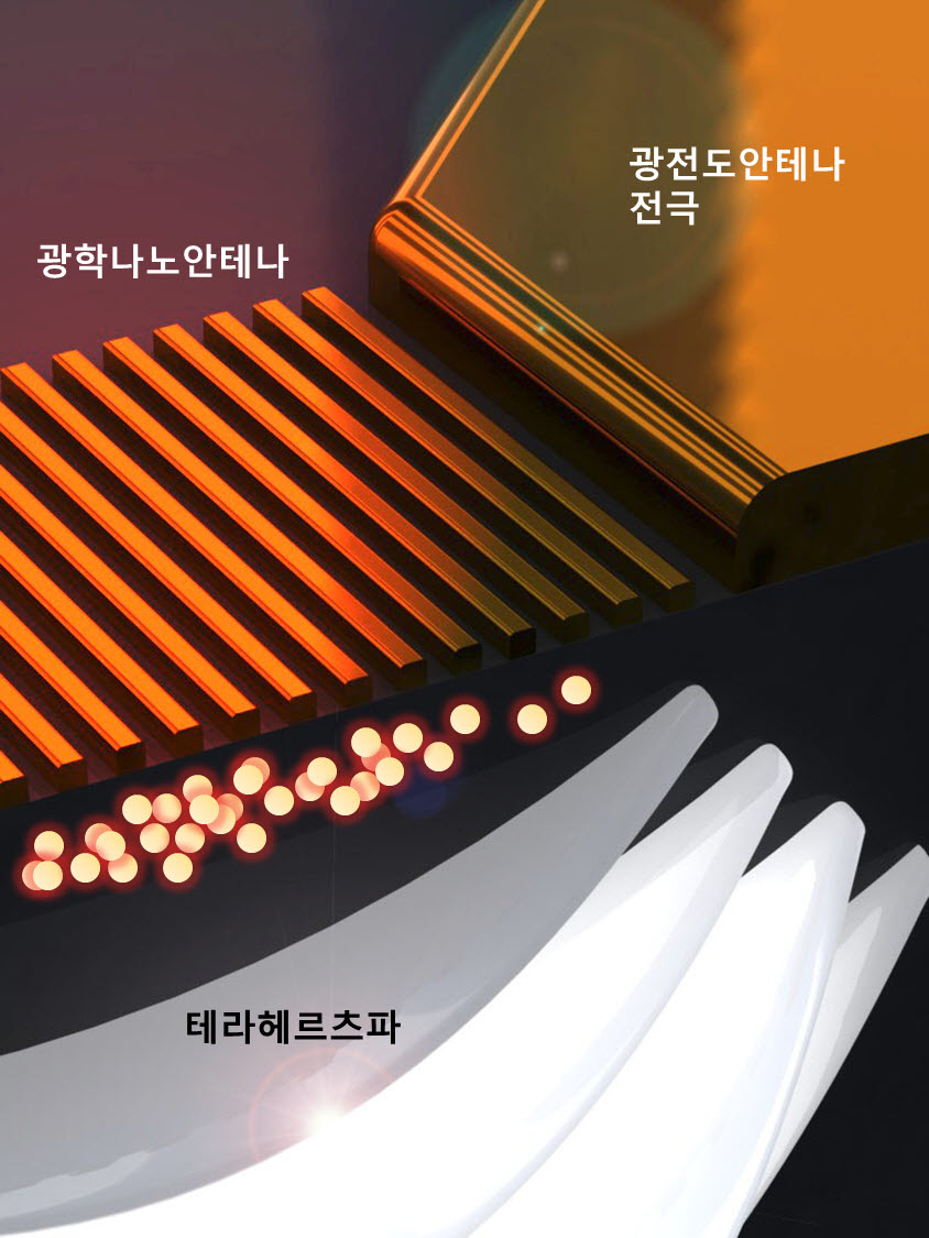 The output of terahertz waves enhanced by KAIST team
KAIST researchers have greatly improved the output of terahertz waves, the blue ocean of the optics world. This technology is expected to be applied to portable X-ray cameras, small bio-diagnostic systems, and in many other devices.
Professor Ki-Hun Jeong"s research team from the Department of Bio and Brain Engineering used optical nano-antenna technology to increase the output of terahertz waves by three times.
Terahertz waves are electromagnetic waves with frequencies between 100GHz to 30THz. They are produced when a femtosecond (10^-15 s) pulse laser is shone on a semiconductor substrate with photoconduction antennas, causing a photocurrent pulse of one picosecond (10^-12 s). Their long wavelengths, in comparison to visible light and infrared rays, give terahertz waves a high penetration power with less energy than X-rays, making them less harmful to humans.
These qualities allow us to see through objects, just as X-rays do, but because terahertz waves absorb certain frequencies, we can detect hidden explosives or drugs, which was not possible with X-rays. We can even identify fake drugs. Furthermore, using the spectral information, we can analyze a material"s innate qualities without chemical processing, making it possible to identify skin diseases without harming the body. However, the output was not sufficient to be used in biosensors and other applications.
Prof. Jeong"s team added optical nano-antennas, made from gold nano-rods, in between the photoconduction antennas and optimized the structure. This resulted in nanoplasmonic resonance in the photoconduction substrate, increasing the degree of integration of the photocurrent pulse and resulting in a three times larger output.
Hence, it is not only possible to see through objects more clearly, but it is also possible to analyze components without a biopsy.
Professor Jeong explained, "This technology, coupled with the miniaturization of terahertz devices, can be applied to endoscopes to detect early epithelial cancer" and that he will focus on creating and commercializing these biosensor systems.
This research was published in the March issue of the international nanotechnology journal ACS Nano and was funded by the Korea Evaluation Institute of Industrial Technology and the National Research Foundation of Korea.
Figure: Mimetic diagram of a THz generator with nano-antennas
2012.04.29 View 9797
The output of terahertz waves enhanced by KAIST team
KAIST researchers have greatly improved the output of terahertz waves, the blue ocean of the optics world. This technology is expected to be applied to portable X-ray cameras, small bio-diagnostic systems, and in many other devices.
Professor Ki-Hun Jeong"s research team from the Department of Bio and Brain Engineering used optical nano-antenna technology to increase the output of terahertz waves by three times.
Terahertz waves are electromagnetic waves with frequencies between 100GHz to 30THz. They are produced when a femtosecond (10^-15 s) pulse laser is shone on a semiconductor substrate with photoconduction antennas, causing a photocurrent pulse of one picosecond (10^-12 s). Their long wavelengths, in comparison to visible light and infrared rays, give terahertz waves a high penetration power with less energy than X-rays, making them less harmful to humans.
These qualities allow us to see through objects, just as X-rays do, but because terahertz waves absorb certain frequencies, we can detect hidden explosives or drugs, which was not possible with X-rays. We can even identify fake drugs. Furthermore, using the spectral information, we can analyze a material"s innate qualities without chemical processing, making it possible to identify skin diseases without harming the body. However, the output was not sufficient to be used in biosensors and other applications.
Prof. Jeong"s team added optical nano-antennas, made from gold nano-rods, in between the photoconduction antennas and optimized the structure. This resulted in nanoplasmonic resonance in the photoconduction substrate, increasing the degree of integration of the photocurrent pulse and resulting in a three times larger output.
Hence, it is not only possible to see through objects more clearly, but it is also possible to analyze components without a biopsy.
Professor Jeong explained, "This technology, coupled with the miniaturization of terahertz devices, can be applied to endoscopes to detect early epithelial cancer" and that he will focus on creating and commercializing these biosensor systems.
This research was published in the March issue of the international nanotechnology journal ACS Nano and was funded by the Korea Evaluation Institute of Industrial Technology and the National Research Foundation of Korea.
Figure: Mimetic diagram of a THz generator with nano-antennas
2012.04.29 View 9797 -
Inexpensive Separation Method of Graphene Developed
The problem with commercializing graphene that is synthesized onto metals over a wide area is that it can not be separated from the metal. However, a groundbreaking separation technology which is both cheap and environment friendly has been developed.
Prof. Taek soo Kim and Prof. Byung Jin Cho"s research teams have conducted this research under the support of the Global Frontier program and Researcher Support Program initiated by The Ministry of Education and Science and Korea Research Foundation. The research results have been posted on the online news flash of Nano Letters on februrary 29th. (Thesis title: Direct Measurement of Adhesion Energy of Monolayer Graphene As-Grown on Copper and Its Application to Renewable Transfer Process)
The research has generated exact results on the interfacial adhesive energy of graphene and its surface material for the first time. Through this, the catalyst metal are no longer to be used just once, but will be used for an infinite number of times, thereby being ecofriendly and efficient.
Wide area graphine synthesized onto the catalyst meatal are used in various ways such as for display and for solar cells. There has been much research going on in this field. However, in order to use this wide area graphene, the graphene must be removed from the catalyst metal without damage.
Until now, the metal had been melted away through the use of chemical substances in order to separate the graphene. However, this method has been very problematic. The metal can not be reused, the costs are very high, much harmful wastes were created in the process of melting the metals, and the process was very complicated.
The research teams of Professors Taek Su Kim and Byung Jin Cho measured the interfacial adhesive energy of the synthesized graphene and learned that it could be easily removed.
Also, the mechanically removed graphene was successfully used in creating molecular electronic devices directly. This has thus innovatively shortened the graphene manufacturing process. Also, it has been confirmed that the metalic board can be reused multiple times after the graphene is removed. A new, ecofriendly and cost friendly method of graphene manufacturing has been paved.
Through this discovery, it is expected that graphene will become easier to manufacture and that the period til the commercialization date of graphene will therefore be greatly reduced
Prof. Cho stated " This reserach has much academical meaning significance in that it has successfully defined the surfacial adhesive energy between the graphene and its catalyst material and it should receive much attention in that it solved the largest technical problem involved in the production of graphene.
2012.04.04 View 10844
-
A Step Closer to Ultra Slim Mobile Phone
Professor Baek Kyung Wook (department of Material Science and Engineering) succeeded in developing an ultra-thin conjugation technique that can perfectly replace the modular contact in electronic devices.
The research team developed a compound material using ultra-fine solder-adhesive film and developed the vertical ultrasonic conjugation process thereby making a reliable utra-thin conjugation.
The developed technique allowed for very thin and reliable conjugation and will be able to replace the socket type connector and is expected to revolutionize the electronic device industry.
In mobile electronic devices like the smartphone, the trend is to incorporate various functional modules like camera, display, touchscreens, etc. in addition to striving for miniaturization of the device.
Recently the problem was the fact that the number of modules within the device was increasing due to the incorporation of various functions, and consequently the volume that these modules took up increased as well, which made miniaturization almost impossible.
Professor Baek‘s team succeeded in improving upon this problem by creating a compound material that has ultra-fine solder particles that can melt to form alloy fusion with the electrode and thermosetting adhesive film that can wrap around the electrode and provide mechanical protection.
The use of this material made it possible to reduce the thickness of the connector by hundredth fold which improved electrical, mechanical properties and highly reliable.
From a processing standpoint the conventional conjugation process involved heating the mechanical block and was therefore hard to manage its production and also consumed 1000W and took up to 15 seconds.
By contrast, Professor Baek’s team’s new process uses only ultrasound to locally heat and melt the conjugation point itself thereby reducing power consumption to 100W and conjugation time to 1~5 seconds.
The technique developed by Professor Baek and Lee Ki Won Doctorate student was awarded Excellent Dissertation Award by world famous journals like the Electronic Components and Technology Conference and is being recognized worldwide.
2012.01.31 View 7621
-
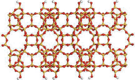 Ten Breakthroughs of the Year 2011 by Science
Porous Zeolite Crytals
Science, an internationally renowned scientific journal based in the US, has recently released a special issue of “Breakthrough of the Year, 2011,” dated December 23, 2011. In the issue, the journal introduces ten most important research breakthroughs made this year, and Professor Ryong Ryoo, Department of Chemistry at KAIST, was one of the scientists behind such notable advancements in 2011. Professor Ryoo has been highly regarded internationally for his research on the development of synthetic version of zeolites, a family of porous minerals that is widely used for products such as laundry detergents, cat litters, etc. Below is the article from Science, stating the zeolite research:
For Science’s “Breakthrough of the Year, 2011”, please go to:
http://www.sciencemag.org/site/special/btoy2011/
[Excerpt from the December 23, 2011 Issue of Science]
Industrial Molecules, Tailor-Made
If you ever doubt that chemistry is still a creative endeavor, just look at zeolites. This family of porous minerals was first discovered in 1756. They"re formed from different arrangements of aluminum, silicon, and oxygen atoms that crystallize into holey structures pocked with a perfect arrangement of pores. Over the past 250 years, 40 natural zeolites have been discovered, and chemists have chipped in roughly 150 more synthetic versions.
View larger version:
In this page
In a new window
Assembly required.
Porous zeolite crystals are widely used as filters and catalysts. This year, researchers found new ways to tailor the size of their pores and create thinner, cheaper membranes.
CREDIT: K. VAROON ET AL., SCIENCE334, 6052 (7 OCTOBER 2001)
This abundance isn"t just for show. Three million tons of zeolites are produced every year for use in laundry detergents, cat litter, and many other products. But zeolites really strut their stuff in two uses: as catalysts and molecular sieves. Oil refineries use zeolite catalysts to break down long hydrocarbon chains in oil into the shorter, volatile hydrocarbons in gasoline. And the minerals" small, regularly arranged pores make them ideal filters for purifying everything from the air on spaceships to the contaminated water around the nuclear reactors destroyed earlier this year in Fukushima, Japan.
Zeolites have their limitations, though. Their pores are almost universally tiny, making it tough to use them as catalysts for large molecules. And they"re difficult to form into ultrathin membranes, which researchers would like to do to enable cheaper separations. But progress by numerous teams on zeolite synthesis this year gave this “mature” area of chemistry new life.
Researchers in South Korea crafted a family of zeolites in which the usual network of small pores is surrounded by walls holed with larger voids. That combination of large and small pores should lead to catalysts for numerous large organic molecules.
Labs in Spain and China produced related large- and small-pore zeolites by using a combination of inorganic and organic materials to guide the structures as they formed.
Meanwhile, researchers in France and Germany discovered that, by carefully controlling growth conditions, they could form a large-pore zeolite without the need for the expensive organic compounds typically used to guide their architecture as they grow. The advance opens the way for cheaper catalysts. In yet another lab, researchers in Minnesota came up with a new route for making ultrathin zeolite membranes, which are likely to be useful as a wide variety of chemically selective filters.
This surge of molecular wizardry provides a vivid reminder that the creativity of chemists keeps their field ever young.
Related References and Web Sites
2011.12.23 View 10109
Ten Breakthroughs of the Year 2011 by Science
Porous Zeolite Crytals
Science, an internationally renowned scientific journal based in the US, has recently released a special issue of “Breakthrough of the Year, 2011,” dated December 23, 2011. In the issue, the journal introduces ten most important research breakthroughs made this year, and Professor Ryong Ryoo, Department of Chemistry at KAIST, was one of the scientists behind such notable advancements in 2011. Professor Ryoo has been highly regarded internationally for his research on the development of synthetic version of zeolites, a family of porous minerals that is widely used for products such as laundry detergents, cat litters, etc. Below is the article from Science, stating the zeolite research:
For Science’s “Breakthrough of the Year, 2011”, please go to:
http://www.sciencemag.org/site/special/btoy2011/
[Excerpt from the December 23, 2011 Issue of Science]
Industrial Molecules, Tailor-Made
If you ever doubt that chemistry is still a creative endeavor, just look at zeolites. This family of porous minerals was first discovered in 1756. They"re formed from different arrangements of aluminum, silicon, and oxygen atoms that crystallize into holey structures pocked with a perfect arrangement of pores. Over the past 250 years, 40 natural zeolites have been discovered, and chemists have chipped in roughly 150 more synthetic versions.
View larger version:
In this page
In a new window
Assembly required.
Porous zeolite crystals are widely used as filters and catalysts. This year, researchers found new ways to tailor the size of their pores and create thinner, cheaper membranes.
CREDIT: K. VAROON ET AL., SCIENCE334, 6052 (7 OCTOBER 2001)
This abundance isn"t just for show. Three million tons of zeolites are produced every year for use in laundry detergents, cat litter, and many other products. But zeolites really strut their stuff in two uses: as catalysts and molecular sieves. Oil refineries use zeolite catalysts to break down long hydrocarbon chains in oil into the shorter, volatile hydrocarbons in gasoline. And the minerals" small, regularly arranged pores make them ideal filters for purifying everything from the air on spaceships to the contaminated water around the nuclear reactors destroyed earlier this year in Fukushima, Japan.
Zeolites have their limitations, though. Their pores are almost universally tiny, making it tough to use them as catalysts for large molecules. And they"re difficult to form into ultrathin membranes, which researchers would like to do to enable cheaper separations. But progress by numerous teams on zeolite synthesis this year gave this “mature” area of chemistry new life.
Researchers in South Korea crafted a family of zeolites in which the usual network of small pores is surrounded by walls holed with larger voids. That combination of large and small pores should lead to catalysts for numerous large organic molecules.
Labs in Spain and China produced related large- and small-pore zeolites by using a combination of inorganic and organic materials to guide the structures as they formed.
Meanwhile, researchers in France and Germany discovered that, by carefully controlling growth conditions, they could form a large-pore zeolite without the need for the expensive organic compounds typically used to guide their architecture as they grow. The advance opens the way for cheaper catalysts. In yet another lab, researchers in Minnesota came up with a new route for making ultrathin zeolite membranes, which are likely to be useful as a wide variety of chemically selective filters.
This surge of molecular wizardry provides a vivid reminder that the creativity of chemists keeps their field ever young.
Related References and Web Sites
2011.12.23 View 10109 -
Spintronics: A high wire act by Nanowerk News
An article by Nanowerk News on the integration of ferromagnetic nanowire arrays on grapheme substrates was published. Professor Bong-Soo Kim from the Department of Chemistry, KAIST, led the research in conjunction with Hanyang University and Samsung in Korea.
http://www.nanowerk.com/news/newsid=22204.php
Posted: Jul 25th, 2011
Spintronics: A high wire act
(Nanowerk News) Graphene is a promising material for a wide range of applications due to its remarkable mechanical and electronic properties. An application of particular interest is spin-based electronics, or spintronics, in which the spin orientation of an electron is used to perform circuit functions in addition to its charge. Bongsoo Kim and colleagues from KAIST, Hanyang University and Samsung in Korea now report the integration of ferromagnetic nanowire arrays on graphene substrates, opening up a route for the construction of graphene-based spintronic devices using nanowires as spin-injecting contacts ("Epitaxially Integrating Ferromagnetic Fe1.3Ge Nanowire Arrays on Few-Layer Graphene").
The spin of an electron is a property that, like charge, can be used to encode, process and transport information. However, spin information is easily lost in most media, which has made spintronics difficult to realize in practice. In graphene, on the other hand, spin can be preserved for longer due to its peculiar electron transport properties. "Low intrinsic spin–orbit coupling, long spin diffusion lengths and vanishing hyperfine interaction are features of graphene that make it a promising medium for spin transport," explains Kim.
Scanning electron microscopy image of vertical iron germanide nanowires grown on graphene. (© ACS 2011)
A prerequisite for the realization of spintronic devices based on graphene is its integration with ferromagnetic contacts to allow spin injection. Kim and his co-workers found that nanowires of iron germanide (Fe1.3Ge) serve as efficient contacts for this purpose. "Iron germanide nanowires show low resistivity and room-temperature ferromagnetism, and they are compatible with existing complementary metal–oxide–semiconductor technologies," says Kim.
To produce the atomically well-defined interfacial contact between the nanowires and the graphene surface needed for optimum device performance, the researchers deposited the contacts by an epitaxial method based on chemical vapor transport. Through careful adjustment of deposition parameters such as carrier gas flow rate and reaction temperature, the researchers produced vertically aligned nanowires that are closely lattice-matched to the graphene sheets (see image).
Initially preparing the graphene sheets on a substrate of silicon oxide allowed the researchers to isolate the final nanowire–graphene structure by etching and then transfer it to another substrate, greatly expanding the versatility of the approach. It is a delicate process, however. "It is necessary to transfer the graphene films onto the substrate very carefully in order to avoid folding and wrinkling of the graphene," says Kim.
Source: Tokyo Institute of Technology
2011.07.26 View 9248
-
Biomimetic Carbon Nanotube Fiber Synthesis Technology Developed
The byssus of the mussel allows it to live in harsh conditions where it is constantly battered by crashing waves by allowing the mussel to latch onto the seaside rocks. This particular characteristic of the mussel is due to the unique structure and high adhesiveness of the mussel’s byssus.
KAIST’s Professor Hong Soon Hyung (Department of Material Science and Engineering) and Professor Lee Hae Shin (Department of Chemistry) and the late Professor Park Tae Kwan (Department of Bio Engineering) were able to reproduce the mussel’s byssus using carbon nanotubes.
The carbon nanotube, since its discovery in 1991, was regarded as the next generation material due to its electrical, thermal, and mechanical properties. However due to its short length of several nanometers, its industrial use was limited.
The KAIST research team referred to the structure of the byssus of the mussel to solve this problem.
The byssus is composed of collagen fibers and Mefp-1 protein which are in a cross-linking structure. The Mefp-1 protein has catecholamine that allows it to bind strongly with the collagen fiber.
In the artificial structure, the carbon nanotube took on the role of the collagen fibers and the macromolecular adhesive took on the role of the catecholamine. The result was a fiber that was ultra-light and ultra-strong.
The results of the experiment were published in the Advanced Materials magazine and is patent registered both domestically and internationally.
2011.06.20 View 10322