Nano
-
 A Transport Technology for Nanowires Thermally Treated at 700 Celsius Degrees
Professor Jun-Bo Yoon and his research team of the Department of Electrical Engineering at KAIST developed a technology for transporting thermally treated nanowires to a flexible substrate and created a high performance device for collecting flexible energy by using the new technology.
Mr. Min-Ho Seo, a Ph.D. candidate, participated in this study as the first author. The results were published online on January 30th in ACS Nano, an international journal in the field of nanoscience and engineering. (“Versatile Transfer of an Ultralong and Seamless Nanowire Array Crystallized at High Temperature for Use in High-performance Flexible Devices,” DOI: 10.1021/acsnano.6b06842)
Nanowires are one of the most representative nanomaterials. They have wire structures with dimensions in nanometers. The nanowires are widely used in the scientific and engineering fields due to their prominent physical and chemical properties that depend on a one-dimensional structure, and their high applicability.
Nanowires have much higher performance if their structure has unique features such as an excellent arrangement and a longer-than-average length. Many researchers are thus actively participating in the research for making nanowires without much difficulty, analyzing them, and developing them for high performance application devices.
Scientists have recently favored a research topic on making nanowires chemically and physically on a flexible substrate and applies the nanowires to a flexible electric device such as a high performance wearable sensor.
The existing technology, however, mixed nanowires from a chemical synthesis with a solution and spread the mixture on a flexible substrate. The resultant distribution was random, and it was difficult to produce a high performance device based on the structural advantages of nanowires. In addition, the technology used a cutting edge nano-process and flexible materials, but this was not economically beneficial. The production of stable materials at a temperature of 700 Celsius degrees or higher is unattainable, a great challenge for the application.
To solve this problem, the research team developed a new nano-transfer technology that combines a silicon nano-grating board with a large surface area and a nano-sacrificial layer process. A nano-sacrificial layer exists between nanowires and a nano-grating board, which acts as the mold for the nano-transfer. The new technology allows the device undergo thermal treatment. After this, the layer disappears when the nanowires are transported to a flexible substrate.
This technology also permits the stable production of nanowires with secured properties at an extremely high temperature. In this case, the nanowires are neatly organized on a flexible substrate. The research team used the technology to manufacture barium carbonate nanowires on top of the flexible substrate. The wires secured their properties at a temperature of 700℃ or above. The team employed the collection of wearable energy to obtain much higher electrical energy than that of an energy collecting device designed based on regular barium titanate nanowires.
The researchers said that their technology is built upon a semiconductor process, known as Physical Vapor Deposition that allows various materials such as ceramics and semiconductors to be used for flexible substrates of nanowires. They expected that high performance flexible electric devices such as flexible transistors and thermoelectric elements can be produced with this method.
Mr. Seo said, “In this study, we transported nanowire materials with developed properties on a flexible substrate and showed an increase in device performance. Our technology will be fundamental to the production of various nanowires on a flexible substrate as well as the feasibility of making high performance wearable electric devices.”
This research was supported by the Leap Research Support Program of the National Research Foundation of Korea.
Fig. 1. Transcription process of new, developed nanowires (a) and a fundamental mimetic diagram of a nano-sacrificial layer (b)
Fig. 2. Transcription results from using gold (AU) nanowires. The categories of the results were (a) optical images, (b) physical signals, (c) cross-sectional images from a scanning electron microscope (SEM), and (d-f) an electric verification of whether the perfectly arranged nanowires were made on a large surface.
Fig. 3. Transcription from using barium titanate (BaTiO3) nanowires. The results were (a) optical images, (b-e) top images taken from an SEM in various locations, and (f, g) property analysis.
Fig. 4. Mimetic diagram of the energy collecting device from using a BaTiO3 nanowire substrate and an optical image of the experiment for the miniature energy collecting device attached to an index finger.
2017.03.22 View 7257
A Transport Technology for Nanowires Thermally Treated at 700 Celsius Degrees
Professor Jun-Bo Yoon and his research team of the Department of Electrical Engineering at KAIST developed a technology for transporting thermally treated nanowires to a flexible substrate and created a high performance device for collecting flexible energy by using the new technology.
Mr. Min-Ho Seo, a Ph.D. candidate, participated in this study as the first author. The results were published online on January 30th in ACS Nano, an international journal in the field of nanoscience and engineering. (“Versatile Transfer of an Ultralong and Seamless Nanowire Array Crystallized at High Temperature for Use in High-performance Flexible Devices,” DOI: 10.1021/acsnano.6b06842)
Nanowires are one of the most representative nanomaterials. They have wire structures with dimensions in nanometers. The nanowires are widely used in the scientific and engineering fields due to their prominent physical and chemical properties that depend on a one-dimensional structure, and their high applicability.
Nanowires have much higher performance if their structure has unique features such as an excellent arrangement and a longer-than-average length. Many researchers are thus actively participating in the research for making nanowires without much difficulty, analyzing them, and developing them for high performance application devices.
Scientists have recently favored a research topic on making nanowires chemically and physically on a flexible substrate and applies the nanowires to a flexible electric device such as a high performance wearable sensor.
The existing technology, however, mixed nanowires from a chemical synthesis with a solution and spread the mixture on a flexible substrate. The resultant distribution was random, and it was difficult to produce a high performance device based on the structural advantages of nanowires. In addition, the technology used a cutting edge nano-process and flexible materials, but this was not economically beneficial. The production of stable materials at a temperature of 700 Celsius degrees or higher is unattainable, a great challenge for the application.
To solve this problem, the research team developed a new nano-transfer technology that combines a silicon nano-grating board with a large surface area and a nano-sacrificial layer process. A nano-sacrificial layer exists between nanowires and a nano-grating board, which acts as the mold for the nano-transfer. The new technology allows the device undergo thermal treatment. After this, the layer disappears when the nanowires are transported to a flexible substrate.
This technology also permits the stable production of nanowires with secured properties at an extremely high temperature. In this case, the nanowires are neatly organized on a flexible substrate. The research team used the technology to manufacture barium carbonate nanowires on top of the flexible substrate. The wires secured their properties at a temperature of 700℃ or above. The team employed the collection of wearable energy to obtain much higher electrical energy than that of an energy collecting device designed based on regular barium titanate nanowires.
The researchers said that their technology is built upon a semiconductor process, known as Physical Vapor Deposition that allows various materials such as ceramics and semiconductors to be used for flexible substrates of nanowires. They expected that high performance flexible electric devices such as flexible transistors and thermoelectric elements can be produced with this method.
Mr. Seo said, “In this study, we transported nanowire materials with developed properties on a flexible substrate and showed an increase in device performance. Our technology will be fundamental to the production of various nanowires on a flexible substrate as well as the feasibility of making high performance wearable electric devices.”
This research was supported by the Leap Research Support Program of the National Research Foundation of Korea.
Fig. 1. Transcription process of new, developed nanowires (a) and a fundamental mimetic diagram of a nano-sacrificial layer (b)
Fig. 2. Transcription results from using gold (AU) nanowires. The categories of the results were (a) optical images, (b) physical signals, (c) cross-sectional images from a scanning electron microscope (SEM), and (d-f) an electric verification of whether the perfectly arranged nanowires were made on a large surface.
Fig. 3. Transcription from using barium titanate (BaTiO3) nanowires. The results were (a) optical images, (b-e) top images taken from an SEM in various locations, and (f, g) property analysis.
Fig. 4. Mimetic diagram of the energy collecting device from using a BaTiO3 nanowire substrate and an optical image of the experiment for the miniature energy collecting device attached to an index finger.
2017.03.22 View 7257 -
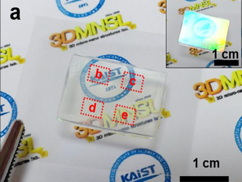
 Semiconductor Photonic Nanocavities on Paper Substrates
Professor Yong-Hoon Cho of the Department of Physics and his team at KAIST have developed a semiconductor photonic nanocavity laser that can operate on a paper substrate.
The researchers hope that this novel method, which involves transferring nano-sized photonic crystal particles onto a paper substrate with high absorptiveness, will enable the diagnoses of various diseases by using high-tech semiconductor sensors at low cost.
The results of this research were published in the November 17th, 2016, issue of Advanced Materials.
Photonic crystals, which utilize light as a medium to provide high bandwidths, can transfer large amounts of information. Compared with their electronic counterparts, photonic crystals also consume less energy to operate.
Normally, semiconductor photonic particles require substrates, which play only a passive role in the assembly and endurance of individual, functional photonic components. These substrates, however, are bulky and environmentally hazardous as they are made up of non-biodegradable materials.
The research team overcame these two shortcomings by replacing a semiconductor substrate with standard paper. The substrate’s mass was reduced considerably, and because paper is made from trees, it degrades. Paper can be easily and cheaply acquired from our surroundings, which drastically reduces the unit cost of semiconductors.
In addition, paper possesses superior mechanical characteristics. It is flexible and can be repeatedly folded and unfolded without being torn. These are traits that have long been sought by researchers for existing flexible substrates.
The research team used a micro-sized stamp to detach photonic crystal nanobeam cavities selectively from their original substrate and transfer them onto a new paper substrate. Using this technique, the team removed nanophotonic crystals that had been patterned (using a process of selectively etching circuits onto a substrate) onto a semiconductor substrate with a high degree of integration, and realigned them as desired on a paper substrate.
The nanophotonic crystals that the team combined with paper in this research were 0.5 micrometers in width, 6 micrometers in length, and 0.3 micrometers in height—about one-hundredth of the width of a single hair (0.1 millimeter).
The team also transferred their photonic crystals onto paper with a fluid channel, which proved that it could be used as a refractive index sensor. As can be seen in current commercial pregnancy diagnosis kits, paper has high absorptiveness. Since photonic crystal particles have high sensitivity, they are highly suitable for applications such as sensors.
Professor Cho stated that “by using paper substrates, this technology can greatly contribute to the rising field of producing environmentally-friendly photonic particles” and “by combining inexpensive paper and high-performance photonic crystal sensors, we can obtain low prices as well as designing appropriate technologies with high performance.”
Dr. Sejeong Kim of the Department of Physics participated in this study as the first author, and Professor Kwanwoo Shin of Sogang University and Professor Yong-Hee Lee of KAIST also took part in this research. The research was supported by the National Research Foundation’s Mid-Career Researcher Program, and the Climate Change Research Hub of KAIST.
Figure 1. Illustration of photonic crystal lasers on paper substrates
Figure 2. Photonic crystal resonator laser and refractive index sensor operating on paper substrates
2017.03.01 View 6224
Semiconductor Photonic Nanocavities on Paper Substrates
Professor Yong-Hoon Cho of the Department of Physics and his team at KAIST have developed a semiconductor photonic nanocavity laser that can operate on a paper substrate.
The researchers hope that this novel method, which involves transferring nano-sized photonic crystal particles onto a paper substrate with high absorptiveness, will enable the diagnoses of various diseases by using high-tech semiconductor sensors at low cost.
The results of this research were published in the November 17th, 2016, issue of Advanced Materials.
Photonic crystals, which utilize light as a medium to provide high bandwidths, can transfer large amounts of information. Compared with their electronic counterparts, photonic crystals also consume less energy to operate.
Normally, semiconductor photonic particles require substrates, which play only a passive role in the assembly and endurance of individual, functional photonic components. These substrates, however, are bulky and environmentally hazardous as they are made up of non-biodegradable materials.
The research team overcame these two shortcomings by replacing a semiconductor substrate with standard paper. The substrate’s mass was reduced considerably, and because paper is made from trees, it degrades. Paper can be easily and cheaply acquired from our surroundings, which drastically reduces the unit cost of semiconductors.
In addition, paper possesses superior mechanical characteristics. It is flexible and can be repeatedly folded and unfolded without being torn. These are traits that have long been sought by researchers for existing flexible substrates.
The research team used a micro-sized stamp to detach photonic crystal nanobeam cavities selectively from their original substrate and transfer them onto a new paper substrate. Using this technique, the team removed nanophotonic crystals that had been patterned (using a process of selectively etching circuits onto a substrate) onto a semiconductor substrate with a high degree of integration, and realigned them as desired on a paper substrate.
The nanophotonic crystals that the team combined with paper in this research were 0.5 micrometers in width, 6 micrometers in length, and 0.3 micrometers in height—about one-hundredth of the width of a single hair (0.1 millimeter).
The team also transferred their photonic crystals onto paper with a fluid channel, which proved that it could be used as a refractive index sensor. As can be seen in current commercial pregnancy diagnosis kits, paper has high absorptiveness. Since photonic crystal particles have high sensitivity, they are highly suitable for applications such as sensors.
Professor Cho stated that “by using paper substrates, this technology can greatly contribute to the rising field of producing environmentally-friendly photonic particles” and “by combining inexpensive paper and high-performance photonic crystal sensors, we can obtain low prices as well as designing appropriate technologies with high performance.”
Dr. Sejeong Kim of the Department of Physics participated in this study as the first author, and Professor Kwanwoo Shin of Sogang University and Professor Yong-Hee Lee of KAIST also took part in this research. The research was supported by the National Research Foundation’s Mid-Career Researcher Program, and the Climate Change Research Hub of KAIST.
Figure 1. Illustration of photonic crystal lasers on paper substrates
Figure 2. Photonic crystal resonator laser and refractive index sensor operating on paper substrates
2017.03.01 View 6224 -
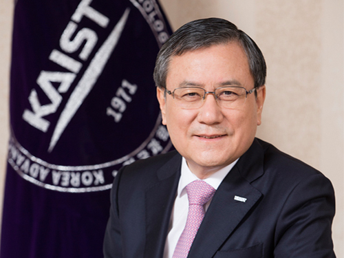 Dr. Sung-Chul Shin Selected 16th President of KAIST
(President Sung-Chul Shin)
The KAIST Board of Trustees elected Professor Sung-Chul Shin of the Department of Physics the 16th president of KAIST on February 21. Professor Shin succeeds President Sung-Mo Kang whose four-year term will end on February 23. He is the first KAIST alumnus to serve as its president.
The Board of Trustees announced, “We believe that Professor Shin’s scientific achievement, outstanding leadership, and clear vision will serve KAIST faculty, students, and staff very well. He will be the best person to help KAIST leap forward in the four years ahead.”
The newly-elected president said, “I am humbled and honored to have been elected to lead such a prestigious institute of Korea. Aiming to be one of the top ten global universities, KAIST will continue to innovate its systems.” Previously, Dr. Shin led the Daegu Gyeongbuk Institute of Science and Technology (DGIST) for six years as president since 2011.
Professor Shin joined the KAIST faculty in 1989. He graduated from Seoul National University and then earned his MS degree in condensed matter physics at KAIST in 1977. After earning his Ph.D. in material physics at Northwestern University in 1984, he worked at Eastman Kodak Research Labs as a senior research scientist for five years.
Before heading to DGIST, President Shin held key administrative positions at KAIST from the early 1990s including dean of planning, dean of the international office, and vice-dean of student affairs. During President Robert Laughlin’s tenure, the first foreign president at KAIST, he served as vice-president for two years from 2004. He also served on the Presidential Advisory Council on Science and Technology of the Korean government as vice chairperson from 2015 to 2016.
A renowned scholar in the field of nanoscience, President Shin’s research focuses on the artificial synthesis and characterization of nonmagnetic materials, magnetic anisotropy, and magneto-optical phenomena. He leads the Laboratory for Nanospinics of Spintronic Materials at KAIST and has published in 290 journals while holding 37 patents.
A fellow in the American Physical Society (APS) since 2008, he was the president of the Korean Physical Society from 2011 to 2012. He has been on the editorial board of J. Magnetism and Magnetic Materials from 2009 and was the first Korean recipient of the Asian Union of Magnetics Societies (AUMS) Award, which recognizes outstanding scientists in the field of magnetics.
President Shin envisions making KAIST’s research and education more competitive through continuing innovation. His innovation efforts will extend to the five key areas of education, research, technology commercialization, globalization, and future planning.
Among his priorities, he emphasizes multidisciplinary studies and leadership training for students. He plans to focus on undeclared major courses for undergraduates to help them expand their experience and exposure to diverse disciplines. This approach will help create well-rounded engineers, scientists, and entrepreneurs by enabling them to develop skills while leveraging a strong connection to the arts, humanities, and social sciences.
To better respond to Industry 4.0, which calls for convergence studies and collaborative work, he proposed establishing a ‘Convergence Innovation System’ by strategically selecting 10 flagship convergence research groups. In order to accelerate the technology commercialization and ecosystem of start-ups, he will strengthen entrepreneurship education, making it a prerequisite requirement for students. President Shin said he will spare no effort to incubate and spin-off ventures in which KAIST technology is being transferred. For globalization efforts, he plans to increase the ratio of foreign faculty from 9 percent to 15 percent, while doubling the current foreign student enrollment ratio of 5 percent. For future strategic innovation, he will implement a long-term innovation strategic plan dubbed ‘Vision 2031.’
2017.02.22 View 7370
Dr. Sung-Chul Shin Selected 16th President of KAIST
(President Sung-Chul Shin)
The KAIST Board of Trustees elected Professor Sung-Chul Shin of the Department of Physics the 16th president of KAIST on February 21. Professor Shin succeeds President Sung-Mo Kang whose four-year term will end on February 23. He is the first KAIST alumnus to serve as its president.
The Board of Trustees announced, “We believe that Professor Shin’s scientific achievement, outstanding leadership, and clear vision will serve KAIST faculty, students, and staff very well. He will be the best person to help KAIST leap forward in the four years ahead.”
The newly-elected president said, “I am humbled and honored to have been elected to lead such a prestigious institute of Korea. Aiming to be one of the top ten global universities, KAIST will continue to innovate its systems.” Previously, Dr. Shin led the Daegu Gyeongbuk Institute of Science and Technology (DGIST) for six years as president since 2011.
Professor Shin joined the KAIST faculty in 1989. He graduated from Seoul National University and then earned his MS degree in condensed matter physics at KAIST in 1977. After earning his Ph.D. in material physics at Northwestern University in 1984, he worked at Eastman Kodak Research Labs as a senior research scientist for five years.
Before heading to DGIST, President Shin held key administrative positions at KAIST from the early 1990s including dean of planning, dean of the international office, and vice-dean of student affairs. During President Robert Laughlin’s tenure, the first foreign president at KAIST, he served as vice-president for two years from 2004. He also served on the Presidential Advisory Council on Science and Technology of the Korean government as vice chairperson from 2015 to 2016.
A renowned scholar in the field of nanoscience, President Shin’s research focuses on the artificial synthesis and characterization of nonmagnetic materials, magnetic anisotropy, and magneto-optical phenomena. He leads the Laboratory for Nanospinics of Spintronic Materials at KAIST and has published in 290 journals while holding 37 patents.
A fellow in the American Physical Society (APS) since 2008, he was the president of the Korean Physical Society from 2011 to 2012. He has been on the editorial board of J. Magnetism and Magnetic Materials from 2009 and was the first Korean recipient of the Asian Union of Magnetics Societies (AUMS) Award, which recognizes outstanding scientists in the field of magnetics.
President Shin envisions making KAIST’s research and education more competitive through continuing innovation. His innovation efforts will extend to the five key areas of education, research, technology commercialization, globalization, and future planning.
Among his priorities, he emphasizes multidisciplinary studies and leadership training for students. He plans to focus on undeclared major courses for undergraduates to help them expand their experience and exposure to diverse disciplines. This approach will help create well-rounded engineers, scientists, and entrepreneurs by enabling them to develop skills while leveraging a strong connection to the arts, humanities, and social sciences.
To better respond to Industry 4.0, which calls for convergence studies and collaborative work, he proposed establishing a ‘Convergence Innovation System’ by strategically selecting 10 flagship convergence research groups. In order to accelerate the technology commercialization and ecosystem of start-ups, he will strengthen entrepreneurship education, making it a prerequisite requirement for students. President Shin said he will spare no effort to incubate and spin-off ventures in which KAIST technology is being transferred. For globalization efforts, he plans to increase the ratio of foreign faculty from 9 percent to 15 percent, while doubling the current foreign student enrollment ratio of 5 percent. For future strategic innovation, he will implement a long-term innovation strategic plan dubbed ‘Vision 2031.’
2017.02.22 View 7370 -
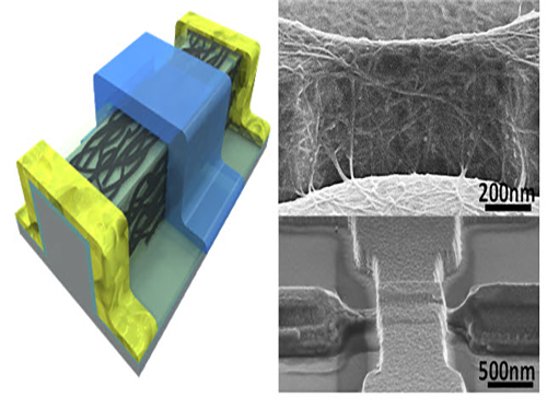 An Improved Carbon Nanotube Semiconductor
Professor Yang-Kyu Choi and his research team of the School of Electrical Engineering at KAIST collaborated with Professor Sung-Jin Choi of Kookmin University to develop a large-scale carbon nanotube semiconductor by using a 3-D fin-gate structure with carbon nanotubes on its top.
Dong Il Lee, a postdoctoral researcher at KAIST’s Electrical Engineering School, participated in this study as the first author. It was published in ACS Nano on November 10, 2016, and was entitled “Three-Dimensional Fin-Structured Semiconducting Carbon Nanotube Network Transistor.”
A semiconductor made with carbon nanotubes operates faster than a silicon semiconductor and requires less energy, yielding higher performance.
Most electronic equipment and devices, however, use silicon semiconductors because it is difficult to fabricate highly purified and densely packed semiconductors with carbon nanotubes (CNTs).
To date, the performance of CNTs was limited due to their low density. Their purity was also low, so it was impossible to make products that had a constant yield on a large-surface wafer or substrate. These characteristics made the mass production of semiconducting CNTs difficult.
To solve these difficulties, the research team used a 3-D fin-gate to vapor-deposit carbon nanotubes on its top. They developed a semiconductor that had a high current density with a width less than 50 nm.
The three-dimensional fin structure was able to vapor-deposit 600 carbon nanotubes per micrometer. This structure could have 20 times more nanotubes than the two dimensional structure, which could only vapor-deposit thirty in the same 1 micrometer width.
In addition, the research team used semi-conductive carbon nanotubes having a purity rating higher than 99.9% from a previous study to obtain a high yield semiconductor.
The semiconductor from the research group has a high current density even with a width less than 50 μm. The new semiconductor is expected to be five times faster than a silicon-based semiconductor and will require five times less electricity during operation.
Furthermore, the new semiconductor can be made by or will be compatible with the equipment for producing silicon-based semiconductors, so there will be no additional costs.
Researcher Lee said, “As a next generation semiconductor, the carbon nanotube semiconductor will have better performance, and its effectiveness will be higher.” He also added, “Hopefully, the new semiconductor will replace the silicon-based semiconductors in ten years.”
This study received support from the Center for Integrated Smart Sensors funded by the Ministry of Science, ICT & Future Planning of Korea as the Global Frontier Project, and from the CMOS (Complementary Metal-Oxide-Semiconductor) THz Technology Convergence Center of the Pioneer Research Center Program sponsored by the National Research Foundation of Korea.
Picture 1: 3D Diagram of the Carbon Nanotube Electronic Device and Its Scanning Electron Microscope (SEM) Image
Picture 2: 3D Transistor Device on an 8-inch Base and the SEM Image of Its Cross Section
2017.02.16 View 8185
An Improved Carbon Nanotube Semiconductor
Professor Yang-Kyu Choi and his research team of the School of Electrical Engineering at KAIST collaborated with Professor Sung-Jin Choi of Kookmin University to develop a large-scale carbon nanotube semiconductor by using a 3-D fin-gate structure with carbon nanotubes on its top.
Dong Il Lee, a postdoctoral researcher at KAIST’s Electrical Engineering School, participated in this study as the first author. It was published in ACS Nano on November 10, 2016, and was entitled “Three-Dimensional Fin-Structured Semiconducting Carbon Nanotube Network Transistor.”
A semiconductor made with carbon nanotubes operates faster than a silicon semiconductor and requires less energy, yielding higher performance.
Most electronic equipment and devices, however, use silicon semiconductors because it is difficult to fabricate highly purified and densely packed semiconductors with carbon nanotubes (CNTs).
To date, the performance of CNTs was limited due to their low density. Their purity was also low, so it was impossible to make products that had a constant yield on a large-surface wafer or substrate. These characteristics made the mass production of semiconducting CNTs difficult.
To solve these difficulties, the research team used a 3-D fin-gate to vapor-deposit carbon nanotubes on its top. They developed a semiconductor that had a high current density with a width less than 50 nm.
The three-dimensional fin structure was able to vapor-deposit 600 carbon nanotubes per micrometer. This structure could have 20 times more nanotubes than the two dimensional structure, which could only vapor-deposit thirty in the same 1 micrometer width.
In addition, the research team used semi-conductive carbon nanotubes having a purity rating higher than 99.9% from a previous study to obtain a high yield semiconductor.
The semiconductor from the research group has a high current density even with a width less than 50 μm. The new semiconductor is expected to be five times faster than a silicon-based semiconductor and will require five times less electricity during operation.
Furthermore, the new semiconductor can be made by or will be compatible with the equipment for producing silicon-based semiconductors, so there will be no additional costs.
Researcher Lee said, “As a next generation semiconductor, the carbon nanotube semiconductor will have better performance, and its effectiveness will be higher.” He also added, “Hopefully, the new semiconductor will replace the silicon-based semiconductors in ten years.”
This study received support from the Center for Integrated Smart Sensors funded by the Ministry of Science, ICT & Future Planning of Korea as the Global Frontier Project, and from the CMOS (Complementary Metal-Oxide-Semiconductor) THz Technology Convergence Center of the Pioneer Research Center Program sponsored by the National Research Foundation of Korea.
Picture 1: 3D Diagram of the Carbon Nanotube Electronic Device and Its Scanning Electron Microscope (SEM) Image
Picture 2: 3D Transistor Device on an 8-inch Base and the SEM Image of Its Cross Section
2017.02.16 View 8185 -
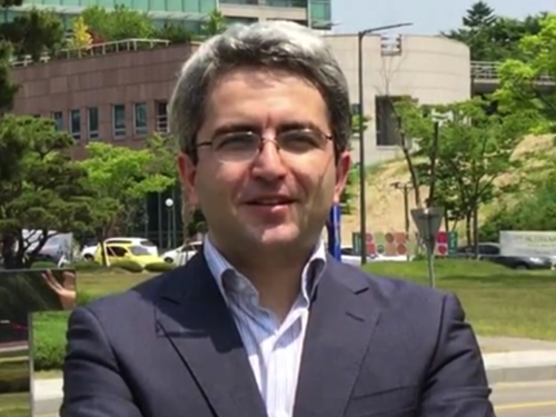 Adsorbent That Can Selectively Remove Water Contaminants
Professor Cafer T. Yavuz and his team at the Graduate School of Energy, Environment, Water, and Sustainability (EEWS) have developed an adsorbent that can selectively capture soluble organic contaminants in water.
This water treatment adsorbent is a fluorine-based nanoporous polymer that can selectively remove water-soluble micromolecules. It has the added advantage of being cheap and easily synthesized, while also being renewable.
The results of this research have been published online in Nature Communication on November 10, 2016. The research paper is titled “Charge-specific Size-dependent Separation of Water-soluble Organic Molecules by Fluorinated Nanoporous Networks.” (DOI: 10.1038/ncomms13377)
Water pollution is accelerating as a result of global industrial development and warming. As new materials are produced and applied in the agricultural and industrial sectors, the types of contaminants expelled as sewage and waste water are also becoming diverse.
Chemicals such as dyes and pesticides can be especially harmful because they are made up of small and highly soluble organic particles that cannot be completely removed during the water treatment process, ultimately ending up in our drinking water.
The current conventional water treatment systems utilize processes such as activated carbon, ozonolysis, and reverse osmosis membrane. These processes, however, are designed to remove larger organic molecules with lower solubility, thus removal of very small molecules with high solubility is difficult. In addition, these micromolecules tend to be charged, therefore are less easily separated in aqueous form.
The research team aimed to remove these small molecules using a new adsorbent technology.
In order to remove aqueous organic molecular contaminants, the team needed an adsorbent that can adsorb micro-sized molecules. It also needed to introduce a chemical function that would allow it to selectively adsorb molecules, and lastly, the adsorbent needed to be structurally stable as it would be used underwater.
The team subsequently developed an adsorbent of fluorine-based porous organic polymer that met all the conditions listed above. By controlling the size of the pores, this adsorbent is able to selectively adsorb aqueous micromolecules of less than 1-2 nm in size.
In addition, in order to separate specific contaminants, there should be a chemical functionality, such as the ability to strongly interact with the target material. Fluorine, the most electronegative atom, interacts strongly with charged soluble organic molecules.
The research team incorporated fluorine into an adsorbent, enabling it to separate charged organic molecules up to 8 times faster than neutral molecules.
The adsorbent developed by Professor Yavuz’s team has wide industrial applications. It can be used in batch-adsorption tests, as well as in column separation for size- and charge-specific adsorption.
Professor Yavuz stated that “the charge-selective properties displayed by fluorine has the potential to be applied in desalination or water treatment processes using membranes."
This paper was first-authored by Dr. Jeehye Byun, and the research was funded by KAIST’s High Risk High Return Program and the Ministry of Science, ICT and Future Planning of Korea’s Mid-Career Researcher Program, as well as its Technology Development Program to Solve Climate Change.
Figure 1. Diagram conceptualizing the process of charge- and size-specific separation by the fluorine-based porous polymer adsorbent
Figure 2. Difference in absorbance before and after using a porous fluorine polymer column to separate organic molecules
Figure 3. Adsorption properties of a fluorine polymer according to the charge and size of organic molecules
2017.01.17 View 8408
Adsorbent That Can Selectively Remove Water Contaminants
Professor Cafer T. Yavuz and his team at the Graduate School of Energy, Environment, Water, and Sustainability (EEWS) have developed an adsorbent that can selectively capture soluble organic contaminants in water.
This water treatment adsorbent is a fluorine-based nanoporous polymer that can selectively remove water-soluble micromolecules. It has the added advantage of being cheap and easily synthesized, while also being renewable.
The results of this research have been published online in Nature Communication on November 10, 2016. The research paper is titled “Charge-specific Size-dependent Separation of Water-soluble Organic Molecules by Fluorinated Nanoporous Networks.” (DOI: 10.1038/ncomms13377)
Water pollution is accelerating as a result of global industrial development and warming. As new materials are produced and applied in the agricultural and industrial sectors, the types of contaminants expelled as sewage and waste water are also becoming diverse.
Chemicals such as dyes and pesticides can be especially harmful because they are made up of small and highly soluble organic particles that cannot be completely removed during the water treatment process, ultimately ending up in our drinking water.
The current conventional water treatment systems utilize processes such as activated carbon, ozonolysis, and reverse osmosis membrane. These processes, however, are designed to remove larger organic molecules with lower solubility, thus removal of very small molecules with high solubility is difficult. In addition, these micromolecules tend to be charged, therefore are less easily separated in aqueous form.
The research team aimed to remove these small molecules using a new adsorbent technology.
In order to remove aqueous organic molecular contaminants, the team needed an adsorbent that can adsorb micro-sized molecules. It also needed to introduce a chemical function that would allow it to selectively adsorb molecules, and lastly, the adsorbent needed to be structurally stable as it would be used underwater.
The team subsequently developed an adsorbent of fluorine-based porous organic polymer that met all the conditions listed above. By controlling the size of the pores, this adsorbent is able to selectively adsorb aqueous micromolecules of less than 1-2 nm in size.
In addition, in order to separate specific contaminants, there should be a chemical functionality, such as the ability to strongly interact with the target material. Fluorine, the most electronegative atom, interacts strongly with charged soluble organic molecules.
The research team incorporated fluorine into an adsorbent, enabling it to separate charged organic molecules up to 8 times faster than neutral molecules.
The adsorbent developed by Professor Yavuz’s team has wide industrial applications. It can be used in batch-adsorption tests, as well as in column separation for size- and charge-specific adsorption.
Professor Yavuz stated that “the charge-selective properties displayed by fluorine has the potential to be applied in desalination or water treatment processes using membranes."
This paper was first-authored by Dr. Jeehye Byun, and the research was funded by KAIST’s High Risk High Return Program and the Ministry of Science, ICT and Future Planning of Korea’s Mid-Career Researcher Program, as well as its Technology Development Program to Solve Climate Change.
Figure 1. Diagram conceptualizing the process of charge- and size-specific separation by the fluorine-based porous polymer adsorbent
Figure 2. Difference in absorbance before and after using a porous fluorine polymer column to separate organic molecules
Figure 3. Adsorption properties of a fluorine polymer according to the charge and size of organic molecules
2017.01.17 View 8408 -
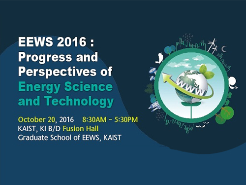 2016 KAIST EEWS Workshop
The Energy, Environment, Water and Sustainability (EEWS) Graduate School of KAIST hosted a workshop entitled “Progress and Perspectives of Energy Science and Technology” on October 20, 2016. The workshop took place at the Fusion Hall of the KAIST Institute on campus.
About 400 experts in energy science and engineering participated in the event. Eight globally recognized scientists introduced the latest research trends in nanomaterials, energy theory, catalysts, and photocatalysts and led discussions on the current status and prospects of EEWS.
Professors Yi Cui of Stanford University, an expert in nanomaterials, and William A. Goddard of California Institute of Technology presented their research experiments on materials design and recent results on the direction of theory under the topics of energy and environment.
Dr. Miquel Salmeron, a former head of the Material Science Division of Lawrence Berkeley National Laboratory, and Professor Yuichi Ikuhara of Tokyo University introduced their analysis of catalysts and energy matters at an atomic scale.
Professor Sukbok Chang of the Chemistry Department at KAIST, a deputy editor of ACS Catalysis and the head of the Center for Catalytic Hydrocarbon Functionalizations at the Institute of Basic Science, and Professor Yang-Kook Sun of Energy Engineering at Hanyang University, who is also a deputy editor of ACS Energy Letters, presented their latest research results on new catalytic reaction development and energy storage.
The workshop consisted of three sections which addressed the design of energy and environment materials; analysis of energy and catalytic materials; and energy conversion and catalysts.
The EEWS Graduate School was established in 2008 with the sponsorship of the Korean government’s World Class University (WCU) project to support science education in Korea. Professor J. Fraser Stoddart, the winner of the 2016 Nobel Prize in Chemistry, was previously worked at the KAIST EEWS Graduate School as a WCU visiting professor for two years, from 2011 to 2013. Professor Ali Coskun, who was a postdoctoral researcher in the laboratory of Professor Stoddart, now teaches and conducts research as a full-time professor at the graduate school.
Dean Yousung Jung of the EEWS Graduate School said:
“This workshop has provided us with a meaningful opportunity to engage in discussions on energy science and technology with world-class scholars from all around the world. It is also a good venue for our graduate school to share with them what we have been doing in research and education.”
2016.10.20 View 8765
2016 KAIST EEWS Workshop
The Energy, Environment, Water and Sustainability (EEWS) Graduate School of KAIST hosted a workshop entitled “Progress and Perspectives of Energy Science and Technology” on October 20, 2016. The workshop took place at the Fusion Hall of the KAIST Institute on campus.
About 400 experts in energy science and engineering participated in the event. Eight globally recognized scientists introduced the latest research trends in nanomaterials, energy theory, catalysts, and photocatalysts and led discussions on the current status and prospects of EEWS.
Professors Yi Cui of Stanford University, an expert in nanomaterials, and William A. Goddard of California Institute of Technology presented their research experiments on materials design and recent results on the direction of theory under the topics of energy and environment.
Dr. Miquel Salmeron, a former head of the Material Science Division of Lawrence Berkeley National Laboratory, and Professor Yuichi Ikuhara of Tokyo University introduced their analysis of catalysts and energy matters at an atomic scale.
Professor Sukbok Chang of the Chemistry Department at KAIST, a deputy editor of ACS Catalysis and the head of the Center for Catalytic Hydrocarbon Functionalizations at the Institute of Basic Science, and Professor Yang-Kook Sun of Energy Engineering at Hanyang University, who is also a deputy editor of ACS Energy Letters, presented their latest research results on new catalytic reaction development and energy storage.
The workshop consisted of three sections which addressed the design of energy and environment materials; analysis of energy and catalytic materials; and energy conversion and catalysts.
The EEWS Graduate School was established in 2008 with the sponsorship of the Korean government’s World Class University (WCU) project to support science education in Korea. Professor J. Fraser Stoddart, the winner of the 2016 Nobel Prize in Chemistry, was previously worked at the KAIST EEWS Graduate School as a WCU visiting professor for two years, from 2011 to 2013. Professor Ali Coskun, who was a postdoctoral researcher in the laboratory of Professor Stoddart, now teaches and conducts research as a full-time professor at the graduate school.
Dean Yousung Jung of the EEWS Graduate School said:
“This workshop has provided us with a meaningful opportunity to engage in discussions on energy science and technology with world-class scholars from all around the world. It is also a good venue for our graduate school to share with them what we have been doing in research and education.”
2016.10.20 View 8765 -
 Professor Keon-Jae Lee Lectures at IEDM and ISSCC Forums
Professor Keon-Jae Lee of KAIST’s Materials Science and Engineering Department delivered a speech at the 2015 Institute of Electrical and Electronics Engineers (IEEE) International Electron Devices Meeting (IEDM) held on December 7-9, 2015 in Washington, D.C.
He will also present a speech at the 2016 International Solid-State Circuits Conference scheduled on January 31-February 4, 2016 in San Francisco, California.
Both professional gatherings are considered the world’s most renowned forums in electronic devices and semiconductor technology. It is rare for a Korean researcher to be invited to speak at these global conferences.
Professor Lee was recognized for his research on flexible NAND chips. The Korea Times, an English language daily newspaper in Korea, reported on his participation in the forums and his recent work. An excerpt of the article follows below:
“KAIST Professor to Lecture at Renowned Tech Forums”
By Lee Min-hyung, The Korea Times, November 26, 2015
Recently he has focused on delivering technologies for producing flexible materials that can be applied to everyday life. The flexible NAND flash memory chips are expected to be widely used for developing flexible handsets. His latest research also includes flexible light-emitting diodes (LED) for implantable biomedical applications.
Lee is currently running a special laboratory focused on developing new flexible nano-materials. The research group is working to develop what it calls “self-powered flexible electronic systems” using nanomaterials and electronic technology.
Lee’s achievement with flexible NAND chips was published in the October edition of Nano Letters, the renowned U.S.-based scientific journal.
He said that flexible memory chips will be used to develop wearable computers that can be installed anywhere.
2015.11.26 View 7401
Professor Keon-Jae Lee Lectures at IEDM and ISSCC Forums
Professor Keon-Jae Lee of KAIST’s Materials Science and Engineering Department delivered a speech at the 2015 Institute of Electrical and Electronics Engineers (IEEE) International Electron Devices Meeting (IEDM) held on December 7-9, 2015 in Washington, D.C.
He will also present a speech at the 2016 International Solid-State Circuits Conference scheduled on January 31-February 4, 2016 in San Francisco, California.
Both professional gatherings are considered the world’s most renowned forums in electronic devices and semiconductor technology. It is rare for a Korean researcher to be invited to speak at these global conferences.
Professor Lee was recognized for his research on flexible NAND chips. The Korea Times, an English language daily newspaper in Korea, reported on his participation in the forums and his recent work. An excerpt of the article follows below:
“KAIST Professor to Lecture at Renowned Tech Forums”
By Lee Min-hyung, The Korea Times, November 26, 2015
Recently he has focused on delivering technologies for producing flexible materials that can be applied to everyday life. The flexible NAND flash memory chips are expected to be widely used for developing flexible handsets. His latest research also includes flexible light-emitting diodes (LED) for implantable biomedical applications.
Lee is currently running a special laboratory focused on developing new flexible nano-materials. The research group is working to develop what it calls “self-powered flexible electronic systems” using nanomaterials and electronic technology.
Lee’s achievement with flexible NAND chips was published in the October edition of Nano Letters, the renowned U.S.-based scientific journal.
He said that flexible memory chips will be used to develop wearable computers that can be installed anywhere.
2015.11.26 View 7401 -
 Membrane
Scientists at KAIST have developed a new way of making fuel cell membranes using nanoscale fasteners, paving the way for lower-cost, higher-efficiency and more easily manufactured fuel cells.
The internal workings of fuel cells vary, but basically all types mix hydrogen and oxygen to produce a chemical reaction that delivers usable electricity and exhausts ordinary water as a by-product. One of the most efficient types is the proton exchange membrane (PEM) fuel cell, which operates at low enough temperatures to be used in homes and vehicles.
To generate electricity, PEM fuel cells rely on two chemical compartments separated by a permeable catalyst membrane. This membrane acts as an electrolyte; a negative electrode is bonded to one side of the membrane and a positive electrode is bonded to the other. The electrolyte membrane is often based on a polymer of perfluorosulfonic acid. Due to its high cost, however, a less expensive hydrocarbon-based electrolyte membrane has attracted interest in this technology sector.
Until now, the challenge in adopting such a hydrocarbon membrane has been that the interface between the electrode and hydrocarbon membrane is weak. This causes the membrane to delaminate relatively easily, falling apart and losing efficiency with use.
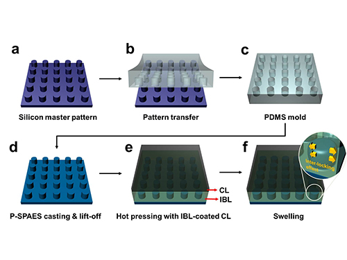
Professor Hee-Tak Kim of the Department of Chemical and Biomolecular Engineering at the Korea Advanced Institute of Science and Technology (KAIST) and his research team have developed a new fastening system that bonds the two materials mechanically rather than chemically. This opens the way to the development of fuel cell membranes that are less expensive, easier to manufacture, stronger and more efficient.
The researchers achieved this by moulding a pattern of tiny cylindrical pillars on the face of the hydrocarbon membrane. The pillars protrude into a softened skin of the electrode with heat. The mechanical bond sets and strengthens as the material cools and absorbs water. The pillar-patterned hydrocarbon membrane is cast using silicone moulds.
Professor Kim said, “This physically fastened bond is almost five times stronger and harder to separate than current bonds between the same layers.”
The new interlocking method also appears to offer a way to bond many types of hydrocarbon membranes that, until now, have been rejected because they couldn’t be fastened robustly. This would make hydrocarbon membranes practical for a number of applications beyond fuel cells such as rechargeable “redox flow” batteries.
The research team is now developing a stronger and more scalable interlocking interface for their nanoscale fasteners.
Picture: Schematic Diagram of the Fabrication of the Pillar P-SPAES Membrane and Its Working Principle of Interlocking Effects
2015.11.06 View 9074
Membrane
Scientists at KAIST have developed a new way of making fuel cell membranes using nanoscale fasteners, paving the way for lower-cost, higher-efficiency and more easily manufactured fuel cells.
The internal workings of fuel cells vary, but basically all types mix hydrogen and oxygen to produce a chemical reaction that delivers usable electricity and exhausts ordinary water as a by-product. One of the most efficient types is the proton exchange membrane (PEM) fuel cell, which operates at low enough temperatures to be used in homes and vehicles.
To generate electricity, PEM fuel cells rely on two chemical compartments separated by a permeable catalyst membrane. This membrane acts as an electrolyte; a negative electrode is bonded to one side of the membrane and a positive electrode is bonded to the other. The electrolyte membrane is often based on a polymer of perfluorosulfonic acid. Due to its high cost, however, a less expensive hydrocarbon-based electrolyte membrane has attracted interest in this technology sector.
Until now, the challenge in adopting such a hydrocarbon membrane has been that the interface between the electrode and hydrocarbon membrane is weak. This causes the membrane to delaminate relatively easily, falling apart and losing efficiency with use.
Professor Hee-Tak Kim of the Department of Chemical and Biomolecular Engineering at the Korea Advanced Institute of Science and Technology (KAIST) and his research team have developed a new fastening system that bonds the two materials mechanically rather than chemically. This opens the way to the development of fuel cell membranes that are less expensive, easier to manufacture, stronger and more efficient.
The researchers achieved this by moulding a pattern of tiny cylindrical pillars on the face of the hydrocarbon membrane. The pillars protrude into a softened skin of the electrode with heat. The mechanical bond sets and strengthens as the material cools and absorbs water. The pillar-patterned hydrocarbon membrane is cast using silicone moulds.
Professor Kim said, “This physically fastened bond is almost five times stronger and harder to separate than current bonds between the same layers.”
The new interlocking method also appears to offer a way to bond many types of hydrocarbon membranes that, until now, have been rejected because they couldn’t be fastened robustly. This would make hydrocarbon membranes practical for a number of applications beyond fuel cells such as rechargeable “redox flow” batteries.
The research team is now developing a stronger and more scalable interlocking interface for their nanoscale fasteners.
Picture: Schematic Diagram of the Fabrication of the Pillar P-SPAES Membrane and Its Working Principle of Interlocking Effects
2015.11.06 View 9074 -
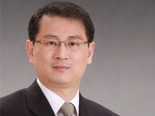
 Professor Kyoungsik Yu Receives the Young IT Engineer Award from IEEE and IEIE of Korea
Professor Kyoungsik Yu of KAIST’s Department of Electrical Engineering is the recipient of this year’s Young IT (Information Technology) Engineer Award that was co-hosted by the Institute of Electrical and Electronics Engineers (IEEE), the Institute of Electronics Engineers of Korea (IEIE), and Haedong Science Culture Foundation in Korea. The award was presented on June 22, 2015 at The Ramada Plaza Jeju Hotel on Jeju Island, Korea.
The Young IT Engineer Award is given to emerging scientists who have made significant contributions to the advancement of technology, society, environment, and creative education.
Professor Yu's main research interests are IT, energy, and imaging through miniaturization and integration of optoelectronic devices. His contribution to academic and technological development is reflected in his publication of more than 100 papers in international journals and conferences, which were cited over 2,200 times.
Professor Yu said, “I’m honored to receive this award and am encouraged by it. I also find the award meaningful because the United Nations has designated this year as the “International Year of Light and Light-based Technologies,” the field I have been involved in as a researcher.”
In addition to Korea, the IEEE has jointly hosted and presented this award to researchers in countries such as Chile, Ecuador, Peru, Singapore, and Italy.
2015.06.22 View 8151
Professor Kyoungsik Yu Receives the Young IT Engineer Award from IEEE and IEIE of Korea
Professor Kyoungsik Yu of KAIST’s Department of Electrical Engineering is the recipient of this year’s Young IT (Information Technology) Engineer Award that was co-hosted by the Institute of Electrical and Electronics Engineers (IEEE), the Institute of Electronics Engineers of Korea (IEIE), and Haedong Science Culture Foundation in Korea. The award was presented on June 22, 2015 at The Ramada Plaza Jeju Hotel on Jeju Island, Korea.
The Young IT Engineer Award is given to emerging scientists who have made significant contributions to the advancement of technology, society, environment, and creative education.
Professor Yu's main research interests are IT, energy, and imaging through miniaturization and integration of optoelectronic devices. His contribution to academic and technological development is reflected in his publication of more than 100 papers in international journals and conferences, which were cited over 2,200 times.
Professor Yu said, “I’m honored to receive this award and am encouraged by it. I also find the award meaningful because the United Nations has designated this year as the “International Year of Light and Light-based Technologies,” the field I have been involved in as a researcher.”
In addition to Korea, the IEEE has jointly hosted and presented this award to researchers in countries such as Chile, Ecuador, Peru, Singapore, and Italy.
2015.06.22 View 8151 -
 Professor Sang Ouk Kim Receives the POSCO Academic Award
Professor Sang Ouk Kim of KAIST’s Department of Materials Science and Engineering received the 2015 POSCO Academic Award. The award ceremony took place at the annual conference of the Korean Institute of Metals and Materials on April 23, 2015.
The POSCO Academic Award has been presented to the Institute's researchers and academics in recognition of their contributions to the advancement of metals and materials engineering in Korea.
Professor Kim is known for his pioneering work in manipulating the properties (work function, conductivity, surface energy, chemo-responsiveness, etc.) of carbon-based materials using double-element doping. Through his research, Professor Kim showed that carbon materials could be extremely useful in various areas including solar batteries and flexible devices. His work has been recognized and published in such journals as Advanced Materials, which invited him to write a review paper on his research in its 25th anniversary issue in 2014, along with world-renowned scholars including the Nobel laureate Alan Heeger.
Professor Kim has published a total of 143 Science Citation Index papers in journals like Nature, Science, Nature Materials, Nature Communications, Advanced Materials, Nano Letters, and Physical Review Letters. According to Scopus, a bibliographic database containing abstracts and citations for academic journal articles, he has been cited 6,456 times and has the h-index of 44, an index describing the scientific productivity and impact of a researcher.
2015.04.22 View 8681
Professor Sang Ouk Kim Receives the POSCO Academic Award
Professor Sang Ouk Kim of KAIST’s Department of Materials Science and Engineering received the 2015 POSCO Academic Award. The award ceremony took place at the annual conference of the Korean Institute of Metals and Materials on April 23, 2015.
The POSCO Academic Award has been presented to the Institute's researchers and academics in recognition of their contributions to the advancement of metals and materials engineering in Korea.
Professor Kim is known for his pioneering work in manipulating the properties (work function, conductivity, surface energy, chemo-responsiveness, etc.) of carbon-based materials using double-element doping. Through his research, Professor Kim showed that carbon materials could be extremely useful in various areas including solar batteries and flexible devices. His work has been recognized and published in such journals as Advanced Materials, which invited him to write a review paper on his research in its 25th anniversary issue in 2014, along with world-renowned scholars including the Nobel laureate Alan Heeger.
Professor Kim has published a total of 143 Science Citation Index papers in journals like Nature, Science, Nature Materials, Nature Communications, Advanced Materials, Nano Letters, and Physical Review Letters. According to Scopus, a bibliographic database containing abstracts and citations for academic journal articles, he has been cited 6,456 times and has the h-index of 44, an index describing the scientific productivity and impact of a researcher.
2015.04.22 View 8681 -
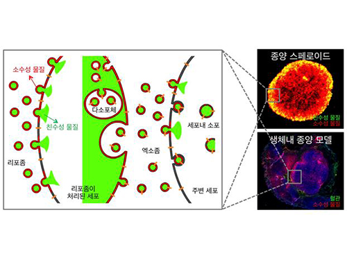 Anti-Cancer Therapy Delivering Drug to an Entire Tumor Developed
KAIST’s Department of Bio and Brain Engineering Professor Ji-Ho Park and his team successfully developed a new highly efficacious anti-cancer nanotechnology by delivering anti-cancer drugs uniformly to an entire tumor. Their research results were published in Nano Letters online on March 31, 2015.
To treat inoperable tumors, anti-cancer medicine is commonly used. However, efficient drug delivery to tumor cells is often difficult, treating an entire tumor with drugs even more so.
Using the existing drug delivery systems, including nanotechnology, a drug can be delivered only to tumor cells near blood vessels, leaving cells at the heart of a tumor intact. Since most drugs are injected into the bloodstream, tumor recurrence post medication is frequent.
Therefore, the team used liposomes that can fuse to the cell membrane and enter the cell. Once inside liposomes the drug can travel into the bloodstream, enter tumor cells near blood vessels, where they are loaded to exosomes, which are naturally occurring nanoparticles in the body. Since exosomes can travel between cells, the drug can be delivered efficiently into inner cells of the tumor.
Exosomes, which are secreted by cells that exist in the tumor microenvironment, is known to have an important role in tumor progression and metastasis since they transfer biological materials between cells. The research team started the investigation recognizing the possibility of delivering the anti-cancer drug to the entire tumor using exosomes.
The team injected the light-sensitive anti-cancer drug using their new delivery technique into experimental mice. The researchers applied light to the tumor site to activate the anti-cancer treatment and analyzed a tissue sample. They observed the effects of the anti-cancer drug in the entire tumor tissue.
The team’s results establish a ground-breaking foothold in drug delivery technology development that can be tailored to specific diseases by understanding its microenvironment. The work paves the way to more effective drug delivery systems for many chronic diseases, including cancer tumors that were difficult to treat due to the inability to penetrate deep into the tissue.
The team is currently conducting experiments with other anti-cancer drugs, which are being developed by pharmaceutical companies, using their tumor-penetrating drug delivery nanotechnology, to identify its effects on malignant tumors.
Professor Park said, “This research is the first to apply biological nanoparticles, exosomes that are continuously secreted and can transfer materials to neighboring cells, to deliver drugs directly to the heart of tumor.”
Picture: Incorporation of hydrophilic and hydrophobic compounds into membrane vesicles by engineering the parental cells via synthetic liposomes.
2015.04.07 View 10029
Anti-Cancer Therapy Delivering Drug to an Entire Tumor Developed
KAIST’s Department of Bio and Brain Engineering Professor Ji-Ho Park and his team successfully developed a new highly efficacious anti-cancer nanotechnology by delivering anti-cancer drugs uniformly to an entire tumor. Their research results were published in Nano Letters online on March 31, 2015.
To treat inoperable tumors, anti-cancer medicine is commonly used. However, efficient drug delivery to tumor cells is often difficult, treating an entire tumor with drugs even more so.
Using the existing drug delivery systems, including nanotechnology, a drug can be delivered only to tumor cells near blood vessels, leaving cells at the heart of a tumor intact. Since most drugs are injected into the bloodstream, tumor recurrence post medication is frequent.
Therefore, the team used liposomes that can fuse to the cell membrane and enter the cell. Once inside liposomes the drug can travel into the bloodstream, enter tumor cells near blood vessels, where they are loaded to exosomes, which are naturally occurring nanoparticles in the body. Since exosomes can travel between cells, the drug can be delivered efficiently into inner cells of the tumor.
Exosomes, which are secreted by cells that exist in the tumor microenvironment, is known to have an important role in tumor progression and metastasis since they transfer biological materials between cells. The research team started the investigation recognizing the possibility of delivering the anti-cancer drug to the entire tumor using exosomes.
The team injected the light-sensitive anti-cancer drug using their new delivery technique into experimental mice. The researchers applied light to the tumor site to activate the anti-cancer treatment and analyzed a tissue sample. They observed the effects of the anti-cancer drug in the entire tumor tissue.
The team’s results establish a ground-breaking foothold in drug delivery technology development that can be tailored to specific diseases by understanding its microenvironment. The work paves the way to more effective drug delivery systems for many chronic diseases, including cancer tumors that were difficult to treat due to the inability to penetrate deep into the tissue.
The team is currently conducting experiments with other anti-cancer drugs, which are being developed by pharmaceutical companies, using their tumor-penetrating drug delivery nanotechnology, to identify its effects on malignant tumors.
Professor Park said, “This research is the first to apply biological nanoparticles, exosomes that are continuously secreted and can transfer materials to neighboring cells, to deliver drugs directly to the heart of tumor.”
Picture: Incorporation of hydrophilic and hydrophobic compounds into membrane vesicles by engineering the parental cells via synthetic liposomes.
2015.04.07 View 10029 -
 Professor Sangyong Jon Appointed Fellow of AIMBE
Professor Sangyong Jon of the Department of Biological Sciences at KAIST has been appointed a member of the American Institute for Medical and Biological Engineering (AIMBE) fellowship.
Established in 1991, AIMBE is a non-profit organization based in Washington, D.C., representing 50,000 individuals and the top 2% of medical and biological engineers. AIMBE provides policy advice and advocacy for medical and biological engineering for the benefit of humanity. It has had about 1,500 fellows over the past 25 years. Among the members, only 110 are non-American nationalities.
Following the appointment of Dr. Hae-Bang Lee, the former senior researcher at the Korean Research Institute of Chemical Technology, and Distinguished Professor Sang Yup Lee of the Department of Chemical and Biomolecular Engineering at KAIST, Professor Jon is the third Korean to become an AIMBE fellow. He had an induction ceremony for the appointment of his fellowship at the AIMBE’s Annual Event held on March 15-17, 2015 in Washington, D.C.
An authority on nanomedicine, Professor Jon has developed many original technologies including multi-functional Theranostics nano particles for the diagnosis and treatment of diseases. He received the Most Cited Paper Award from Theranostics, an academic journal specialized in nanomedicine, last February.
Additionally, Professor Jon is a leading researcher in the field of translational medicine, using a multi-disciplinary, highly collaborative, “Bench to Bedside” approach for disease treatment and prevention. He created a biotechnology venture company and transferred research developments to the industry in Korea.
2015.03.12 View 9932
Professor Sangyong Jon Appointed Fellow of AIMBE
Professor Sangyong Jon of the Department of Biological Sciences at KAIST has been appointed a member of the American Institute for Medical and Biological Engineering (AIMBE) fellowship.
Established in 1991, AIMBE is a non-profit organization based in Washington, D.C., representing 50,000 individuals and the top 2% of medical and biological engineers. AIMBE provides policy advice and advocacy for medical and biological engineering for the benefit of humanity. It has had about 1,500 fellows over the past 25 years. Among the members, only 110 are non-American nationalities.
Following the appointment of Dr. Hae-Bang Lee, the former senior researcher at the Korean Research Institute of Chemical Technology, and Distinguished Professor Sang Yup Lee of the Department of Chemical and Biomolecular Engineering at KAIST, Professor Jon is the third Korean to become an AIMBE fellow. He had an induction ceremony for the appointment of his fellowship at the AIMBE’s Annual Event held on March 15-17, 2015 in Washington, D.C.
An authority on nanomedicine, Professor Jon has developed many original technologies including multi-functional Theranostics nano particles for the diagnosis and treatment of diseases. He received the Most Cited Paper Award from Theranostics, an academic journal specialized in nanomedicine, last February.
Additionally, Professor Jon is a leading researcher in the field of translational medicine, using a multi-disciplinary, highly collaborative, “Bench to Bedside” approach for disease treatment and prevention. He created a biotechnology venture company and transferred research developments to the industry in Korea.
2015.03.12 View 9932