Nano
-
 Quantum Emitters: Beyond Crystal Clear to Single-Photon Pure
‘Nanoscale Focus Pinspot’ can quench only the background noise without changing the optical properties of the quantum emitter and the built-in photonic structure
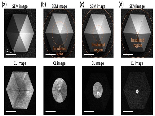
Photons, fundamental particles of light, are carrying these words to your eyes via the light from your computer screen or phone. Photons play a key role in the next-generation quantum information technology, such as quantum computing and communications. A quantum emitter, capable of producing a single, pure photon, is the crux of such technology but has many issues that have yet to be solved, according to KAIST researchers.
A research team under Professor Yong-Hoon Cho has developed a technique that can isolate the desired quality emitter by reducing the noise surrounding the target with what they have dubbed a ‘nanoscale focus pinspot.’ They published their results on June 24 in ACS Nano.
“The nanoscale focus pinspot is a structurally nondestructive technique under an extremely low dose ion beam and is generally applicable for various platforms to improve their single-photon purity while retaining the integrated photonic structures,” said lead author Yong-Hoon Cho from the Department of Physics at KAIST.
To produce single photons from solid state materials, the researchers used wide-bandgap semiconductor quantum dots — fabricated nanoparticles with specialized potential properties, such as the ability to directly inject current into a small chip and to operate at room temperature for practical applications. By making a quantum dot in a photonic structure that propagates light, and then irradiating it with helium ions, researchers theorized that they could develop a quantum emitter that could reduce the unwanted noisy background and produce a single, pure photon on demand.
Professor Cho explained, “Despite its high resolution and versatility, a focused ion beam typically suppresses the optical properties around the bombarded area due to the accelerated ion beam’s high momentum. We focused on the fact that, if the focused ion beam is well controlled, only the background noise can be selectively quenched with high spatial resolution without destroying the structure.”
In other words, the researchers focused the ion beam on a mere pin prick, effectively cutting off the interactions around the quantum dot and removing the physical properties that could negatively interact with and degrade the photon purity emitted from the quantum dot.
“It is the first developed technique that can quench the background noise without changing the optical properties of the quantum emitter and the built-in photonic structure,” Professor Cho asserted.
Professor Cho compared it to stimulated emission depletion microscopy, a technique used to decrease the light around the area of focus, but leaving the focal point illuminated. The result is increased resolution of the desired visual target.
“By adjusting the focused ion beam-irradiated region, we can select the target emitter with nanoscale resolution by quenching the surrounding emitter,” Professor Cho said. “This nanoscale selective-quenching technique can be applied to various material and structural platforms and further extended for applications such as optical memory and high-resolution micro displays.” Korea’s National Research Foundation and the Samsung Science and Technology Foundation supported this work.
-PublicationMinho Choi, Seongmoon Jun, and Yong-Hoon Cho et al. ACS Nano‘Nanoscale Focus Pinspot for High-Purity Quantum Emitters via Focused-Ion-Beam-Induced Luminescence Quenching,’(https://pubs.acs.org/doi/10.1021/acsnano.1c00587)
-ProfileProfessor Yong-Hoon ChoQuantum & Nanobio Photonics Laboratoryhttp://qnp.kaist.ac.kr/
Department of PhysicsKAIST
2021.09.02 View 6022
Quantum Emitters: Beyond Crystal Clear to Single-Photon Pure
‘Nanoscale Focus Pinspot’ can quench only the background noise without changing the optical properties of the quantum emitter and the built-in photonic structure
Photons, fundamental particles of light, are carrying these words to your eyes via the light from your computer screen or phone. Photons play a key role in the next-generation quantum information technology, such as quantum computing and communications. A quantum emitter, capable of producing a single, pure photon, is the crux of such technology but has many issues that have yet to be solved, according to KAIST researchers.
A research team under Professor Yong-Hoon Cho has developed a technique that can isolate the desired quality emitter by reducing the noise surrounding the target with what they have dubbed a ‘nanoscale focus pinspot.’ They published their results on June 24 in ACS Nano.
“The nanoscale focus pinspot is a structurally nondestructive technique under an extremely low dose ion beam and is generally applicable for various platforms to improve their single-photon purity while retaining the integrated photonic structures,” said lead author Yong-Hoon Cho from the Department of Physics at KAIST.
To produce single photons from solid state materials, the researchers used wide-bandgap semiconductor quantum dots — fabricated nanoparticles with specialized potential properties, such as the ability to directly inject current into a small chip and to operate at room temperature for practical applications. By making a quantum dot in a photonic structure that propagates light, and then irradiating it with helium ions, researchers theorized that they could develop a quantum emitter that could reduce the unwanted noisy background and produce a single, pure photon on demand.
Professor Cho explained, “Despite its high resolution and versatility, a focused ion beam typically suppresses the optical properties around the bombarded area due to the accelerated ion beam’s high momentum. We focused on the fact that, if the focused ion beam is well controlled, only the background noise can be selectively quenched with high spatial resolution without destroying the structure.”
In other words, the researchers focused the ion beam on a mere pin prick, effectively cutting off the interactions around the quantum dot and removing the physical properties that could negatively interact with and degrade the photon purity emitted from the quantum dot.
“It is the first developed technique that can quench the background noise without changing the optical properties of the quantum emitter and the built-in photonic structure,” Professor Cho asserted.
Professor Cho compared it to stimulated emission depletion microscopy, a technique used to decrease the light around the area of focus, but leaving the focal point illuminated. The result is increased resolution of the desired visual target.
“By adjusting the focused ion beam-irradiated region, we can select the target emitter with nanoscale resolution by quenching the surrounding emitter,” Professor Cho said. “This nanoscale selective-quenching technique can be applied to various material and structural platforms and further extended for applications such as optical memory and high-resolution micro displays.” Korea’s National Research Foundation and the Samsung Science and Technology Foundation supported this work.
-PublicationMinho Choi, Seongmoon Jun, and Yong-Hoon Cho et al. ACS Nano‘Nanoscale Focus Pinspot for High-Purity Quantum Emitters via Focused-Ion-Beam-Induced Luminescence Quenching,’(https://pubs.acs.org/doi/10.1021/acsnano.1c00587)
-ProfileProfessor Yong-Hoon ChoQuantum & Nanobio Photonics Laboratoryhttp://qnp.kaist.ac.kr/
Department of PhysicsKAIST
2021.09.02 View 6022 -
 Brain-Inspired Highly Scalable Neuromorphic Hardware Presented
Neurons and synapses based on single transistor can dramatically reduce the hardware cost and accelerate the commercialization of neuromorphic hardware
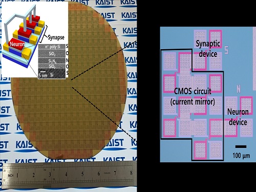
KAIST researchers fabricated a brain-inspired highly scalable neuromorphic hardware by co-integrating single transistor neurons and synapses. Using standard silicon complementary metal-oxide-semiconductor (CMOS) technology, the neuromorphic hardware is expected to reduce chip cost and simplify fabrication procedures.
The research team led by Yang-Kyu Choi and Sung-Yool Choi produced a neurons and synapses based on single transistor for highly scalable neuromorphic hardware and showed the ability to recognize text and face images. This research was featured in Science Advances on August 4.
Neuromorphic hardware has attracted a great deal of attention because of its artificial intelligence functions, but consuming ultra-low power of less than 20 watts by mimicking the human brain. To make neuromorphic hardware work, a neuron that generates a spike when integrating a certain signal, and a synapse remembering the connection between two neurons are necessary, just like the biological brain. However, since neurons and synapses constructed on digital or analog circuits occupy a large space, there is a limit in terms of hardware efficiency and costs. Since the human brain consists of about 1011 neurons and 1014 synapses, it is necessary to improve the hardware cost in order to apply it to mobile and IoT devices.
To solve the problem, the research team mimicked the behavior of biological neurons and synapses with a single transistor, and co-integrated them onto an 8-inch wafer. The manufactured neuromorphic transistors have the same structure as the transistors for memory and logic that are currently mass-produced. In addition, the neuromorphic transistors proved for the first time that they can be implemented with a ‘Janus structure’ that functions as both neuron and synapse, just like coins have heads and tails.
Professor Yang-Kyu Choi said that this work can dramatically reduce the hardware cost by replacing the neurons and synapses that were based on complex digital and analog circuits with a single transistor. "We have demonstrated that neurons and synapses can be implemented using a single transistor," said Joon-Kyu Han, the first author. "By co-integrating single transistor neurons and synapses on the same wafer using a standard CMOS process, the hardware cost of the neuromorphic hardware has been improved, which will accelerate the commercialization of neuromorphic hardware,” Han added.This research was supported by the National Research Foundation (NRF) and IC Design Education Center (IDEC).
-PublicationJoon-Kyu Han, Sung-Yool Choi, Yang-Kyu Choi, et al.“Cointegration of single-transistor neurons and synapses by nanoscale CMOS fabrication for highly scalable neuromorphic hardware,” Science Advances (DOI: 10.1126/sciadv.abg8836)
-ProfileProfessor Yang-Kyu ChoiNano-Oriented Bio-Electronics Labhttps://sites.google.com/view/nobelab/
School of Electrical EngineeringKAIST
Professor Sung-Yool ChoiMolecular and Nano Device Laboratoryhttps://www.mndl.kaist.ac.kr/
School of Electrical EngineeringKAIST
2021.08.05 View 6533
Brain-Inspired Highly Scalable Neuromorphic Hardware Presented
Neurons and synapses based on single transistor can dramatically reduce the hardware cost and accelerate the commercialization of neuromorphic hardware
KAIST researchers fabricated a brain-inspired highly scalable neuromorphic hardware by co-integrating single transistor neurons and synapses. Using standard silicon complementary metal-oxide-semiconductor (CMOS) technology, the neuromorphic hardware is expected to reduce chip cost and simplify fabrication procedures.
The research team led by Yang-Kyu Choi and Sung-Yool Choi produced a neurons and synapses based on single transistor for highly scalable neuromorphic hardware and showed the ability to recognize text and face images. This research was featured in Science Advances on August 4.
Neuromorphic hardware has attracted a great deal of attention because of its artificial intelligence functions, but consuming ultra-low power of less than 20 watts by mimicking the human brain. To make neuromorphic hardware work, a neuron that generates a spike when integrating a certain signal, and a synapse remembering the connection between two neurons are necessary, just like the biological brain. However, since neurons and synapses constructed on digital or analog circuits occupy a large space, there is a limit in terms of hardware efficiency and costs. Since the human brain consists of about 1011 neurons and 1014 synapses, it is necessary to improve the hardware cost in order to apply it to mobile and IoT devices.
To solve the problem, the research team mimicked the behavior of biological neurons and synapses with a single transistor, and co-integrated them onto an 8-inch wafer. The manufactured neuromorphic transistors have the same structure as the transistors for memory and logic that are currently mass-produced. In addition, the neuromorphic transistors proved for the first time that they can be implemented with a ‘Janus structure’ that functions as both neuron and synapse, just like coins have heads and tails.
Professor Yang-Kyu Choi said that this work can dramatically reduce the hardware cost by replacing the neurons and synapses that were based on complex digital and analog circuits with a single transistor. "We have demonstrated that neurons and synapses can be implemented using a single transistor," said Joon-Kyu Han, the first author. "By co-integrating single transistor neurons and synapses on the same wafer using a standard CMOS process, the hardware cost of the neuromorphic hardware has been improved, which will accelerate the commercialization of neuromorphic hardware,” Han added.This research was supported by the National Research Foundation (NRF) and IC Design Education Center (IDEC).
-PublicationJoon-Kyu Han, Sung-Yool Choi, Yang-Kyu Choi, et al.“Cointegration of single-transistor neurons and synapses by nanoscale CMOS fabrication for highly scalable neuromorphic hardware,” Science Advances (DOI: 10.1126/sciadv.abg8836)
-ProfileProfessor Yang-Kyu ChoiNano-Oriented Bio-Electronics Labhttps://sites.google.com/view/nobelab/
School of Electrical EngineeringKAIST
Professor Sung-Yool ChoiMolecular and Nano Device Laboratoryhttps://www.mndl.kaist.ac.kr/
School of Electrical EngineeringKAIST
2021.08.05 View 6533 -
 Quantum Laser Turns Energy Loss into Gain
A new laser that generates quantum particles can recycle lost energy for highly efficient, low threshold laser applications
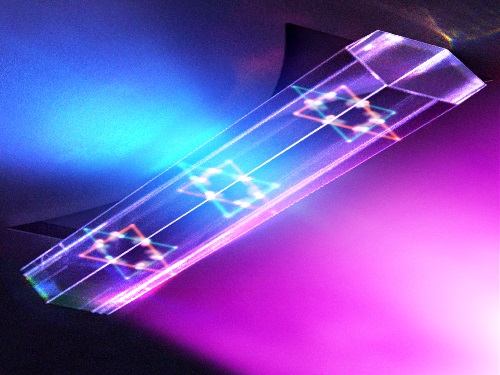
Scientists at KAIST have fabricated a laser system that generates highly interactive quantum particles at room temperature. Their findings, published in the journal Nature Photonics, could lead to a single microcavity laser system that requires lower threshold energy as its energy loss increases.
The system, developed by KAIST physicist Yong-Hoon Cho and colleagues, involves shining light through a single hexagonal-shaped microcavity treated with a loss-modulated silicon nitride substrate. The system design leads to the generation of a polariton laser at room temperature, which is exciting because this usually requires cryogenic temperatures.
The researchers found another unique and counter-intuitive feature of this design. Normally, energy is lost during laser operation. But in this system, as energy loss increased, the amount of energy needed to induce lasing decreased. Exploiting this phenomenon could lead to the development of high efficiency, low threshold lasers for future quantum optical devices.
“This system applies a concept of quantum physics known as parity-time reversal symmetry,” explains Professor Cho. “This is an important platform that allows energy loss to be used as gain. It can be used to reduce laser threshold energy for classical optical devices and sensors, as well as quantum devices and controlling the direction of light.”
The key is the design and materials. The hexagonal microcavity divides light particles into two different modes: one that passes through the upward-facing triangle of the hexagon and another that passes through its downward-facing triangle. Both modes of light particles have the same energy and path but don’t interact with each other.
However, the light particles do interact with other particles called excitons, provided by the hexagonal microcavity, which is made of semiconductors. This interaction leads to the generation of new quantum particles called polaritons that then interact with each other to generate the polariton laser. By controlling the degree of loss between the microcavity and the semiconductor substrate, an intriguing phenomenon arises, with the threshold energy becoming smaller as energy loss increases. This research was supported by the Samsung Science and Technology Foundation and Korea’s National Research Foundation.
-PublicationSong,H.G, Choi, M, Woo, K.Y. Yong-Hoon Cho Room-temperature polaritonic non-Hermitian system with single microcavityNature Photonics (https://doi.org/10.1038/s41566-021-00820-z)
-ProfileProfessor Yong-Hoon ChoQuantum & Nanobio Photonics Laboratoryhttp://qnp.kaist.ac.kr/
Department of PhysicsKAIST
2021.07.07 View 6163
Quantum Laser Turns Energy Loss into Gain
A new laser that generates quantum particles can recycle lost energy for highly efficient, low threshold laser applications
Scientists at KAIST have fabricated a laser system that generates highly interactive quantum particles at room temperature. Their findings, published in the journal Nature Photonics, could lead to a single microcavity laser system that requires lower threshold energy as its energy loss increases.
The system, developed by KAIST physicist Yong-Hoon Cho and colleagues, involves shining light through a single hexagonal-shaped microcavity treated with a loss-modulated silicon nitride substrate. The system design leads to the generation of a polariton laser at room temperature, which is exciting because this usually requires cryogenic temperatures.
The researchers found another unique and counter-intuitive feature of this design. Normally, energy is lost during laser operation. But in this system, as energy loss increased, the amount of energy needed to induce lasing decreased. Exploiting this phenomenon could lead to the development of high efficiency, low threshold lasers for future quantum optical devices.
“This system applies a concept of quantum physics known as parity-time reversal symmetry,” explains Professor Cho. “This is an important platform that allows energy loss to be used as gain. It can be used to reduce laser threshold energy for classical optical devices and sensors, as well as quantum devices and controlling the direction of light.”
The key is the design and materials. The hexagonal microcavity divides light particles into two different modes: one that passes through the upward-facing triangle of the hexagon and another that passes through its downward-facing triangle. Both modes of light particles have the same energy and path but don’t interact with each other.
However, the light particles do interact with other particles called excitons, provided by the hexagonal microcavity, which is made of semiconductors. This interaction leads to the generation of new quantum particles called polaritons that then interact with each other to generate the polariton laser. By controlling the degree of loss between the microcavity and the semiconductor substrate, an intriguing phenomenon arises, with the threshold energy becoming smaller as energy loss increases. This research was supported by the Samsung Science and Technology Foundation and Korea’s National Research Foundation.
-PublicationSong,H.G, Choi, M, Woo, K.Y. Yong-Hoon Cho Room-temperature polaritonic non-Hermitian system with single microcavityNature Photonics (https://doi.org/10.1038/s41566-021-00820-z)
-ProfileProfessor Yong-Hoon ChoQuantum & Nanobio Photonics Laboratoryhttp://qnp.kaist.ac.kr/
Department of PhysicsKAIST
2021.07.07 View 6163 -
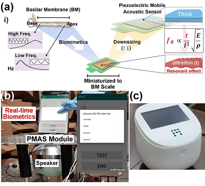 Biomimetic Resonant Acoustic Sensor Detecting Far-Distant Voices Accurately to Hit the Market
A KAIST research team led by Professor Keon Jae Lee from the Department of Materials Science and Engineering has developed a bioinspired flexible piezoelectric acoustic sensor with multi-resonant ultrathin piezoelectric membrane mimicking the basilar membrane of the human cochlea. The flexible acoustic sensor has been miniaturized for embedding into smartphones and the first commercial prototype is ready for accurate and far-distant voice detection.
In 2018, Professor Lee presented the first concept of a flexible piezoelectric acoustic sensor, inspired by the fact that humans can accurately detect far-distant voices using a multi-resonant trapezoidal membrane with 20,000 hair cells. However, previous acoustic sensors could not be integrated into commercial products like smartphones and AI speakers due to their large device size.
In this work, the research team fabricated a mobile-sized acoustic sensor by adopting ultrathin piezoelectric membranes with high sensitivity. Simulation studies proved that the ultrathin polymer underneath inorganic piezoelectric thin film can broaden the resonant bandwidth to cover the entire voice frequency range using seven channels. Based on this theory, the research team successfully demonstrated the miniaturized acoustic sensor mounted in commercial smartphones and AI speakers for machine learning-based biometric authentication and voice processing. (Please refer to the explanatory movie KAIST Flexible Piezoelectric Mobile Acoustic Sensor).
The resonant mobile acoustic sensor has superior sensitivity and multi-channel signals compared to conventional condenser microphones with a single channel, and it has shown highly accurate and far-distant speaker identification with a small amount of voice training data. The error rate of speaker identification was significantly reduced by 56% (with 150 training datasets) and 75% (with 2,800 training datasets) compared to that of a MEMS condenser device.
Professor Lee said, “Recently, Google has been targeting the ‘Wolverine Project’ on far-distant voice separation from multi-users for next-generation AI user interfaces. I expect that our multi-channel resonant acoustic sensor with abundant voice information is the best fit for this application. Currently, the mass production process is on the verge of completion, so we hope that this will be used in our daily lives very soon.”
Professor Lee also established a startup company called Fronics Inc., located both in Korea and U.S. (branch office) to commercialize this flexible acoustic sensor and is seeking collaborations with global AI companies.
These research results entitled “Biomimetic and Flexible Piezoelectric Mobile Acoustic Sensors with Multi-Resonant Ultrathin Structures for Machine Learning Biometrics” were published in Science Advances in 2021 (7, eabe5683).
-Publication
“Biomimetic and flexible piezoelectric mobile acoustic sensors with multiresonant ultrathin structures for machine learning biometrics,” Science Advances (DOI: 10.1126/sciadv.abe5683)
-Profile
Professor Keon Jae Lee
Department of Materials Science and Engineering
Flexible and Nanobio Device Lab
http://fand.kaist.ac.kr/
KAIST
2021.06.14 View 6444
Biomimetic Resonant Acoustic Sensor Detecting Far-Distant Voices Accurately to Hit the Market
A KAIST research team led by Professor Keon Jae Lee from the Department of Materials Science and Engineering has developed a bioinspired flexible piezoelectric acoustic sensor with multi-resonant ultrathin piezoelectric membrane mimicking the basilar membrane of the human cochlea. The flexible acoustic sensor has been miniaturized for embedding into smartphones and the first commercial prototype is ready for accurate and far-distant voice detection.
In 2018, Professor Lee presented the first concept of a flexible piezoelectric acoustic sensor, inspired by the fact that humans can accurately detect far-distant voices using a multi-resonant trapezoidal membrane with 20,000 hair cells. However, previous acoustic sensors could not be integrated into commercial products like smartphones and AI speakers due to their large device size.
In this work, the research team fabricated a mobile-sized acoustic sensor by adopting ultrathin piezoelectric membranes with high sensitivity. Simulation studies proved that the ultrathin polymer underneath inorganic piezoelectric thin film can broaden the resonant bandwidth to cover the entire voice frequency range using seven channels. Based on this theory, the research team successfully demonstrated the miniaturized acoustic sensor mounted in commercial smartphones and AI speakers for machine learning-based biometric authentication and voice processing. (Please refer to the explanatory movie KAIST Flexible Piezoelectric Mobile Acoustic Sensor).
The resonant mobile acoustic sensor has superior sensitivity and multi-channel signals compared to conventional condenser microphones with a single channel, and it has shown highly accurate and far-distant speaker identification with a small amount of voice training data. The error rate of speaker identification was significantly reduced by 56% (with 150 training datasets) and 75% (with 2,800 training datasets) compared to that of a MEMS condenser device.
Professor Lee said, “Recently, Google has been targeting the ‘Wolverine Project’ on far-distant voice separation from multi-users for next-generation AI user interfaces. I expect that our multi-channel resonant acoustic sensor with abundant voice information is the best fit for this application. Currently, the mass production process is on the verge of completion, so we hope that this will be used in our daily lives very soon.”
Professor Lee also established a startup company called Fronics Inc., located both in Korea and U.S. (branch office) to commercialize this flexible acoustic sensor and is seeking collaborations with global AI companies.
These research results entitled “Biomimetic and Flexible Piezoelectric Mobile Acoustic Sensors with Multi-Resonant Ultrathin Structures for Machine Learning Biometrics” were published in Science Advances in 2021 (7, eabe5683).
-Publication
“Biomimetic and flexible piezoelectric mobile acoustic sensors with multiresonant ultrathin structures for machine learning biometrics,” Science Advances (DOI: 10.1126/sciadv.abe5683)
-Profile
Professor Keon Jae Lee
Department of Materials Science and Engineering
Flexible and Nanobio Device Lab
http://fand.kaist.ac.kr/
KAIST
2021.06.14 View 6444 -
 ACS Nano Special Edition Highlights Innovations at KAIST
- The collective intelligence and technological innovation of KAIST was highlighted with case studies including the Post-COVID-19 New Deal R&D Initiative Project. -
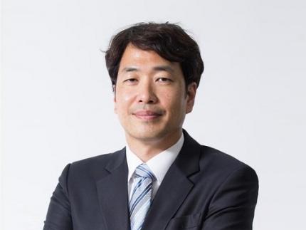
KAIST’s innovative academic achievements and R&D efforts for addressing the world’s greatest challenges such as the COVID-19 pandemic were featured in ACS Nano as part of its special virtual issue commemorating the 50th anniversary of KAIST. The issue consisted of 14 review articles contributed by KAIST faculty from five departments, including two from Professor Il-Doo Kim from the Department of Materials Science and Engineering, who serves as an associate editor of the ACS Nano.
ACS Nano, the leading international journal in nanoscience and nanotechnology, published a special virtual issue last month, titled ‘Celebrating 50 Years of KAIST: Collective Intelligence and Innovation for Confronting Contemporary Issues.’
This special virtual issue introduced KAIST’s vision of becoming a ‘global value-creative leading university’ and its progress toward this vision over the last 50 years. The issue explained how KAIST has served as the main hub for advanced scientific research and technological innovation in South Korea since its establishment in 1971, and how its faculty and over 69,000 graduates played a key role in propelling the nation’s rapid industrialization and economic development.
The issue also emphasized the need for KAIST to enhance global cooperation and the exchange of ideas in the years to come, especially during the post-COVID era intertwined with the Fourth Industrial Revolution (4IR). In this regard, the issue cited the first ‘KAIST Emerging Materials e-Symposium (EMS)’, which was held online for five days in September of last year with a global audience of over 10,000 participating live via Zoom and YouTube, as a successful example of what academic collaboration could look like in the post-COVID and 4IR eras.
In addition, the “Science & Technology New Deal Project for COVID-19 Response,” a project conducted by KAIST with support from the Ministry of Science and ICT (MSIT) of South Korea, was also introduced as another excellent case of KAIST’s collective intelligence and technological innovation. The issue highlighted some key achievements from this project for overcoming the pandemic-driven crisis, such as: reusable anti-virus filters, negative-pressure ambulances for integrated patient transport and hospitalization, and movable and expandable negative-pressure ward modules.
“We hold our expectations high for the outstanding achievements and progress KAIST will have made by its centennial,” said Professor Kim on the background of curating the 14 review articles contributed by KAIST faculty from the fields of Materials Science and Engineering (MSE), Chemical and Biomolecular Engineering (CBE), Nuclear and Quantum Engineering (NQE), Electrical Engineering (EE), and Chemistry (Chem).
Review articles discussing emerging materials and their properties covered photonic carbon dots (Professor Chan Beum Park, MSE), single-atom and ensemble catalysts (Professor Hyunjoo Lee, CBE), and metal/metal oxide electrocatalysts (Professor Sung-Yoon Chung, MSE).
Review articles discussing materials processing covered 2D layered materials synthesis based on interlayer engineering (Professor Kibum Kang, MSE), eco-friendly methods for solar cell production (Professor Bumjoon J. Kim, CBE), an ex-solution process for the synthesis of highly stable catalysts (Professor WooChul Jung, MSE), and 3D light-patterning synthesis of ordered nanostructures (Professor Seokwoo Jeon, MSE, and Professor Dongchan Jang, NQE).
Review articles discussing advanced analysis techniques covered operando materials analyses (Professor Jeong Yeong Park, Chem), graphene liquid cell transmission electron microscopy (Professor Jong Min Yuk, MSE), and multiscale modeling and visualization of materials systems (Professor Seungbum Hong, MSE).
Review articles discussing practical state-of-the-art devices covered chemiresistive hydrogen sensors (Professor Il-Doo Kim, MSE), patient-friendly diagnostics and implantable treatment devices (Professor Steve Park, MSE), triboelectric nanogenerators (Professor Yang-Kyu Choi, EE), and next-generation lithium-air batteries (Professor Hye Ryung Byon, Chem, and Professor Il-Doo Kim, MSE).
In addition to Professor Il-Doo Kim, post-doctoral researcher Dr. Jaewan Ahn from the KAIST Applied Science Research Institute, Dean of the College of Engineering at KAIST Professor Choongsik Bae, and ACS Nano Editor-in-Chief Professor Paul S. Weiss from the University of California, Los Angeles also contributed to the publication of this ACS Nano special virtual issue.
The issue can be viewed and downloaded from the ACS Nano website at https://doi.org/10.1021/acsnano.1c01101.
Image credit: KAIST
Image usage restrictions: News organizations may use or redistribute this image,with proper attribution, as part of news coverage of this paper only.
Publication:
Ahn, J., et al. (2021) Celebrating 50 Years of KAIST: Collective Intelligence and Innovation for Confronting Contemporary Issues. ACS Nano 15(3): 1895-1907. Available online at https://doi.org/10.1021/acsnano.1c01101
Profile:
Il-Doo Kim, Ph.D
Chair Professor
idkim@kaist.ac.kr
http://advnano.kaist.ac.kr
Advanced Nanomaterials and Energy Lab.
Department of Materials Science and Engineering
Membrane Innovation Center for Anti-Virus and Air-Quality Control
https://kaist.ac.kr/
Korea Advanced Institute of Science and Technology (KAIST) Daejeon, Republic of Korea
(END)
2021.03.05 View 19798
ACS Nano Special Edition Highlights Innovations at KAIST
- The collective intelligence and technological innovation of KAIST was highlighted with case studies including the Post-COVID-19 New Deal R&D Initiative Project. -
KAIST’s innovative academic achievements and R&D efforts for addressing the world’s greatest challenges such as the COVID-19 pandemic were featured in ACS Nano as part of its special virtual issue commemorating the 50th anniversary of KAIST. The issue consisted of 14 review articles contributed by KAIST faculty from five departments, including two from Professor Il-Doo Kim from the Department of Materials Science and Engineering, who serves as an associate editor of the ACS Nano.
ACS Nano, the leading international journal in nanoscience and nanotechnology, published a special virtual issue last month, titled ‘Celebrating 50 Years of KAIST: Collective Intelligence and Innovation for Confronting Contemporary Issues.’
This special virtual issue introduced KAIST’s vision of becoming a ‘global value-creative leading university’ and its progress toward this vision over the last 50 years. The issue explained how KAIST has served as the main hub for advanced scientific research and technological innovation in South Korea since its establishment in 1971, and how its faculty and over 69,000 graduates played a key role in propelling the nation’s rapid industrialization and economic development.
The issue also emphasized the need for KAIST to enhance global cooperation and the exchange of ideas in the years to come, especially during the post-COVID era intertwined with the Fourth Industrial Revolution (4IR). In this regard, the issue cited the first ‘KAIST Emerging Materials e-Symposium (EMS)’, which was held online for five days in September of last year with a global audience of over 10,000 participating live via Zoom and YouTube, as a successful example of what academic collaboration could look like in the post-COVID and 4IR eras.
In addition, the “Science & Technology New Deal Project for COVID-19 Response,” a project conducted by KAIST with support from the Ministry of Science and ICT (MSIT) of South Korea, was also introduced as another excellent case of KAIST’s collective intelligence and technological innovation. The issue highlighted some key achievements from this project for overcoming the pandemic-driven crisis, such as: reusable anti-virus filters, negative-pressure ambulances for integrated patient transport and hospitalization, and movable and expandable negative-pressure ward modules.
“We hold our expectations high for the outstanding achievements and progress KAIST will have made by its centennial,” said Professor Kim on the background of curating the 14 review articles contributed by KAIST faculty from the fields of Materials Science and Engineering (MSE), Chemical and Biomolecular Engineering (CBE), Nuclear and Quantum Engineering (NQE), Electrical Engineering (EE), and Chemistry (Chem).
Review articles discussing emerging materials and their properties covered photonic carbon dots (Professor Chan Beum Park, MSE), single-atom and ensemble catalysts (Professor Hyunjoo Lee, CBE), and metal/metal oxide electrocatalysts (Professor Sung-Yoon Chung, MSE).
Review articles discussing materials processing covered 2D layered materials synthesis based on interlayer engineering (Professor Kibum Kang, MSE), eco-friendly methods for solar cell production (Professor Bumjoon J. Kim, CBE), an ex-solution process for the synthesis of highly stable catalysts (Professor WooChul Jung, MSE), and 3D light-patterning synthesis of ordered nanostructures (Professor Seokwoo Jeon, MSE, and Professor Dongchan Jang, NQE).
Review articles discussing advanced analysis techniques covered operando materials analyses (Professor Jeong Yeong Park, Chem), graphene liquid cell transmission electron microscopy (Professor Jong Min Yuk, MSE), and multiscale modeling and visualization of materials systems (Professor Seungbum Hong, MSE).
Review articles discussing practical state-of-the-art devices covered chemiresistive hydrogen sensors (Professor Il-Doo Kim, MSE), patient-friendly diagnostics and implantable treatment devices (Professor Steve Park, MSE), triboelectric nanogenerators (Professor Yang-Kyu Choi, EE), and next-generation lithium-air batteries (Professor Hye Ryung Byon, Chem, and Professor Il-Doo Kim, MSE).
In addition to Professor Il-Doo Kim, post-doctoral researcher Dr. Jaewan Ahn from the KAIST Applied Science Research Institute, Dean of the College of Engineering at KAIST Professor Choongsik Bae, and ACS Nano Editor-in-Chief Professor Paul S. Weiss from the University of California, Los Angeles also contributed to the publication of this ACS Nano special virtual issue.
The issue can be viewed and downloaded from the ACS Nano website at https://doi.org/10.1021/acsnano.1c01101.
Image credit: KAIST
Image usage restrictions: News organizations may use or redistribute this image,with proper attribution, as part of news coverage of this paper only.
Publication:
Ahn, J., et al. (2021) Celebrating 50 Years of KAIST: Collective Intelligence and Innovation for Confronting Contemporary Issues. ACS Nano 15(3): 1895-1907. Available online at https://doi.org/10.1021/acsnano.1c01101
Profile:
Il-Doo Kim, Ph.D
Chair Professor
idkim@kaist.ac.kr
http://advnano.kaist.ac.kr
Advanced Nanomaterials and Energy Lab.
Department of Materials Science and Engineering
Membrane Innovation Center for Anti-Virus and Air-Quality Control
https://kaist.ac.kr/
Korea Advanced Institute of Science and Technology (KAIST) Daejeon, Republic of Korea
(END)
2021.03.05 View 19798 -
 Attachable Skin Monitors that Wick the Sweat Away
- A silicone membrane for wearable devices is more comfortable and breathable thanks to better-sized pores made with the help of citric acid crystals. -
A new preparation technique fabricates thin, silicone-based patches that rapidly wick water away from the skin. The technique could reduce the redness and itching caused by wearable biosensors that trap sweat beneath them. The technique was developed by bioengineer and professor Young-Ho Cho and his colleagues at KAIST and reported in the journal Scientific Reports last month.
“Wearable bioelectronics are becoming more attractive for the day-to-day monitoring of biological compounds found in sweat, like hormones or glucose, as well as body temperature, heart rate, and energy expenditure,” Professor Cho explained. “But currently available materials can cause skin irritation, so scientists are looking for ways to improve them,” he added.
Attachable biosensors often use a silicone-based compound called polydimethylsiloxane (PDMS), as it has a relatively high water vapour transmission rate compared to other materials. Still, this rate is only two-thirds that of skin’s water evaporation rate, meaning sweat still gets trapped underneath it.
Current fabrication approaches mix PDMS with beads or solutes, such as sugars or salts, and then remove them to leave pores in their place. Another technique uses gas to form pores in the material. Each technique has its disadvantages, from being expensive and complex to leaving pores of different sizes.
A team of researchers led by Professor Cho from the KAIST Department of Bio and Brain Engineering was able to form small, uniform pores by crystallizing citric acid in PDMS and then removing the crystals using ethanol. The approach is significantly cheaper than using beads, and leads to 93.2% smaller and 425% more uniformly-sized pores compared to using sugar. Importantly, the membrane transmits water vapour 2.2 times faster than human skin.
The team tested their membrane on human skin for seven days and found that it caused only minor redness and no itching, whereas a non-porous PDMS membrane did.
Professor Cho said, “Our method could be used to fabricate porous PDMS membranes for skin-attachable devices used for daily monitoring of physiological signals.”
“We next plan to modify our membrane so it can be more readily attached to and removed from skin,” he added.
This work was supported by the Ministry of Trade, Industry and Energy (MOTIE) of Korea under the Alchemist Project.
Image description:
Smaller, more uniformly-sized pores are made in the PDMS membrane by mixing PDMS, toluene, citric acid, and ethanol. Toluene dilutes PDMS so it can easily mix with the other two constituents. Toluene and ethanol are then evaporated, which causes the citric acid to crystallize within the PDMS material. The mixture is placed in a mould where it solidifies into a thin film. The crystals are then removed using ethanol, leaving pores in their place.
Image credit:
Professor Young-Ho Cho, KAIST
Image usage restrictions:
News organizations may use or redistribute this image, with proper attribution, as part of news coverage of this paper only.
Publication:
Yoon, S, et al. (2021) Wearable porous PDMS layer of high moisture permeability for skin trouble reduction. Scientific Reports 11, Article No. 938. Available online at https://doi.org/10.1038/s41598-020-78580-z
Profile:
Young-Ho Cho, Ph.D
Professor
mems@kaist.ac.kr
https://mems.kaist.ac.kr
NanoSentuating Systems Laboratory
Department of Bio and Brain Engineering
https://kaist.ac.kr
Korea Advanced Institute of Science and Technology (KAIST)
Daejeon, Republic of Korea
(END)
2021.02.22 View 8369
Attachable Skin Monitors that Wick the Sweat Away
- A silicone membrane for wearable devices is more comfortable and breathable thanks to better-sized pores made with the help of citric acid crystals. -
A new preparation technique fabricates thin, silicone-based patches that rapidly wick water away from the skin. The technique could reduce the redness and itching caused by wearable biosensors that trap sweat beneath them. The technique was developed by bioengineer and professor Young-Ho Cho and his colleagues at KAIST and reported in the journal Scientific Reports last month.
“Wearable bioelectronics are becoming more attractive for the day-to-day monitoring of biological compounds found in sweat, like hormones or glucose, as well as body temperature, heart rate, and energy expenditure,” Professor Cho explained. “But currently available materials can cause skin irritation, so scientists are looking for ways to improve them,” he added.
Attachable biosensors often use a silicone-based compound called polydimethylsiloxane (PDMS), as it has a relatively high water vapour transmission rate compared to other materials. Still, this rate is only two-thirds that of skin’s water evaporation rate, meaning sweat still gets trapped underneath it.
Current fabrication approaches mix PDMS with beads or solutes, such as sugars or salts, and then remove them to leave pores in their place. Another technique uses gas to form pores in the material. Each technique has its disadvantages, from being expensive and complex to leaving pores of different sizes.
A team of researchers led by Professor Cho from the KAIST Department of Bio and Brain Engineering was able to form small, uniform pores by crystallizing citric acid in PDMS and then removing the crystals using ethanol. The approach is significantly cheaper than using beads, and leads to 93.2% smaller and 425% more uniformly-sized pores compared to using sugar. Importantly, the membrane transmits water vapour 2.2 times faster than human skin.
The team tested their membrane on human skin for seven days and found that it caused only minor redness and no itching, whereas a non-porous PDMS membrane did.
Professor Cho said, “Our method could be used to fabricate porous PDMS membranes for skin-attachable devices used for daily monitoring of physiological signals.”
“We next plan to modify our membrane so it can be more readily attached to and removed from skin,” he added.
This work was supported by the Ministry of Trade, Industry and Energy (MOTIE) of Korea under the Alchemist Project.
Image description:
Smaller, more uniformly-sized pores are made in the PDMS membrane by mixing PDMS, toluene, citric acid, and ethanol. Toluene dilutes PDMS so it can easily mix with the other two constituents. Toluene and ethanol are then evaporated, which causes the citric acid to crystallize within the PDMS material. The mixture is placed in a mould where it solidifies into a thin film. The crystals are then removed using ethanol, leaving pores in their place.
Image credit:
Professor Young-Ho Cho, KAIST
Image usage restrictions:
News organizations may use or redistribute this image, with proper attribution, as part of news coverage of this paper only.
Publication:
Yoon, S, et al. (2021) Wearable porous PDMS layer of high moisture permeability for skin trouble reduction. Scientific Reports 11, Article No. 938. Available online at https://doi.org/10.1038/s41598-020-78580-z
Profile:
Young-Ho Cho, Ph.D
Professor
mems@kaist.ac.kr
https://mems.kaist.ac.kr
NanoSentuating Systems Laboratory
Department of Bio and Brain Engineering
https://kaist.ac.kr
Korea Advanced Institute of Science and Technology (KAIST)
Daejeon, Republic of Korea
(END)
2021.02.22 View 8369 -
 Professor Bumjoon Kim Named Scientist of the Month
Professor Bumjoon Kim from the Department of Chemical and Biomolecular Engineering won January’s Scientist of the Month Award presented by the Ministry of Science and ICT (MSIT) and the National Research Foundation of Korea (NRF) on January 6. Professor Kim also received 10 million won in prize money.
Professor Kim was recognized for his research in the field of fuel cells. Since the first paper on fuel cells was published in 1839 by the German chemist Friedrich Schonbein, there has been an increase in the number of fields in which fuel cells are used, including national defense, aerospace engineering, and autonomous vehicles.
Professor Kim developed carbonized block copolymer particles with high durability and a high-performance fuel cell. Block copolymers are two different polymers cross-linked into a chain structure. Various nanostructures can be made effectively by using the attractive and repulsive forces between the chains.
Professor Kim used the membrane emulsification technique, employing a high-performance separation membrane to develop a platform that makes the mass production of highly durable carbonized particles possible, which he then used to develop high-performance energy devices like fuel cells.
The carbonized particles designed by Professor Kim and his research team were used to create the world’s more durable fuel cells that boast outstanding performance while using only five percent of the costly platinum needed for existing commercialized products.
The team’s research results were published in the Journal of the American Chemical Society and Energy Environmental Science in May and July of last year.
“We have developed a fuel cell that ticks all the boxes including performance, durability, and cost,” said Professor Kim. “Related techniques will not be limited to fuel cells, but could also be applied to the development of various energy devices like solar cells and secondary cells,” he added.
(END)
2021.01.22 View 7269
Professor Bumjoon Kim Named Scientist of the Month
Professor Bumjoon Kim from the Department of Chemical and Biomolecular Engineering won January’s Scientist of the Month Award presented by the Ministry of Science and ICT (MSIT) and the National Research Foundation of Korea (NRF) on January 6. Professor Kim also received 10 million won in prize money.
Professor Kim was recognized for his research in the field of fuel cells. Since the first paper on fuel cells was published in 1839 by the German chemist Friedrich Schonbein, there has been an increase in the number of fields in which fuel cells are used, including national defense, aerospace engineering, and autonomous vehicles.
Professor Kim developed carbonized block copolymer particles with high durability and a high-performance fuel cell. Block copolymers are two different polymers cross-linked into a chain structure. Various nanostructures can be made effectively by using the attractive and repulsive forces between the chains.
Professor Kim used the membrane emulsification technique, employing a high-performance separation membrane to develop a platform that makes the mass production of highly durable carbonized particles possible, which he then used to develop high-performance energy devices like fuel cells.
The carbonized particles designed by Professor Kim and his research team were used to create the world’s more durable fuel cells that boast outstanding performance while using only five percent of the costly platinum needed for existing commercialized products.
The team’s research results were published in the Journal of the American Chemical Society and Energy Environmental Science in May and July of last year.
“We have developed a fuel cell that ticks all the boxes including performance, durability, and cost,” said Professor Kim. “Related techniques will not be limited to fuel cells, but could also be applied to the development of various energy devices like solar cells and secondary cells,” he added.
(END)
2021.01.22 View 7269 -
 Chemical Scissors Snip 2D Transition Metal Dichalcogenides into Nanoribbon
New ‘nanoribbon’ catalyst should slash cost of hydrogen production for clean fuels
Researchers have identified a potential catalyst alternative – and an innovative way to produce them using chemical ‘scissors’ – that could make hydrogen production more economical.
The research team led by Professor Sang Ouk Kim at the Department of Materials Science and Engineering published their work in Nature Communications.
Hydrogen is likely to play a key role in the clean transition away from fossil fuels and other processes that produce greenhouse gas emissions. There is a raft of transportation sectors such as long-haul shipping and aviation that are difficult to electrify and so will require cleanly produced hydrogen as a fuel or as a feedstock for other carbon-neutral synthetic fuels. Likewise, fertilizer production and the steel sector are unlikely to be “de-carbonized” without cheap and clean hydrogen.
The problem is that the cheapest methods by far of producing hydrogen gas is currently from natural gas, a process that itself produces the greenhouse gas carbon dioxide–which defeats the purpose.
Alternative techniques of hydrogen production, such as electrolysis using an electric current between two electrodes plunged into water to overcome the chemical bonds holding water together, thereby splitting it into its constituent elements, oxygen and hydrogen are very well established. But one of the factors contributing to the high cost, beyond being extremely energy-intensive, is the need for the very expensive precious and relatively rare metal platinum. The platinum is used as a catalyst–a substance that kicks off or speeds up a chemical reaction–in the hydrogen production process.
As a result, researchers have long been on the hunt for a substitution for platinum -- another catalyst that is abundant in the earth and thus much cheaper.
Transition metal dichalcogenides, or TMDs, in a nanomaterial form, have for some time been considered a good candidate as a catalyst replacement for platinum. These are substances composed of one atom of a transition metal (the elements in the middle part of the periodic table) and two atoms of a chalcogen element (the elements in the third-to-last column in the periodic table, specifically sulfur, selenium and tellurium).
What makes TMDs a good bet as a platinum replacement is not just that they are much more abundant, but also their electrons are structured in a way that gives the electrodes a boost.
In addition, a TMD that is a nanomaterial is essentially a two-dimensional super-thin sheet only a few atoms thick, just like graphene. The ultrathin nature of a 2-D TMD nanosheet allows for a great many more TMD molecules to be exposed during the catalysis process than would be the case in a block of the stuff, thus kicking off and speeding up the hydrogen-making chemical reaction that much more.
However, even here the TMD molecules are only reactive at the four edges of a nanosheet. In the flat interior, not much is going on. In order to increase the chemical reaction rate in the production of hydrogen, the nanosheet would need to be cut into very thin – almost one-dimensional strips, thereby creating many edges.
In response, the research team developed what are in essence a pair of chemical scissors that can snip TMD into tiny strips.
“Up to now, the only substances that anyone has been able to turn into these ‘nano-ribbons’ are graphene and phosphorene,” said Sang Professor Kim, one of the researchers involved in devising the process.
“But they’re both made up of just one element, so it’s pretty straightforward. Figuring out how to do it for TMD, which is made of two elements was going to be much harder.”
The ‘scissors’ involve a two-step process involving first inserting lithium ions into the layered structure of the TMD sheets, and then using ultrasound to cause a spontaneous ‘unzipping’ in straight lines.
“It works sort of like how when you split a plank of plywood: it breaks easily in one direction along the grain,” Professor Kim continued. “It’s actually really simple.”
The researchers then tried it with various types of TMDs, including those made of molybdenum, selenium, sulfur, tellurium and tungsten. All worked just as well, with a catalytic efficiency as effective as platinum’s.
Because of the simplicity of the procedure, this method should be able to be used not just in the large-scale production of TMD nanoribbons, but also to make similar nanoribbons from other multi-elemental 2D materials for purposes beyond just hydrogen production.
-ProfileProfessor Sang Ouk KimSoft Nanomaterials Laboratory (http://snml.kaist.ac.kr)Department of Materials Science and EngineeringKAIST
2020.10.29 View 5273
Chemical Scissors Snip 2D Transition Metal Dichalcogenides into Nanoribbon
New ‘nanoribbon’ catalyst should slash cost of hydrogen production for clean fuels
Researchers have identified a potential catalyst alternative – and an innovative way to produce them using chemical ‘scissors’ – that could make hydrogen production more economical.
The research team led by Professor Sang Ouk Kim at the Department of Materials Science and Engineering published their work in Nature Communications.
Hydrogen is likely to play a key role in the clean transition away from fossil fuels and other processes that produce greenhouse gas emissions. There is a raft of transportation sectors such as long-haul shipping and aviation that are difficult to electrify and so will require cleanly produced hydrogen as a fuel or as a feedstock for other carbon-neutral synthetic fuels. Likewise, fertilizer production and the steel sector are unlikely to be “de-carbonized” without cheap and clean hydrogen.
The problem is that the cheapest methods by far of producing hydrogen gas is currently from natural gas, a process that itself produces the greenhouse gas carbon dioxide–which defeats the purpose.
Alternative techniques of hydrogen production, such as electrolysis using an electric current between two electrodes plunged into water to overcome the chemical bonds holding water together, thereby splitting it into its constituent elements, oxygen and hydrogen are very well established. But one of the factors contributing to the high cost, beyond being extremely energy-intensive, is the need for the very expensive precious and relatively rare metal platinum. The platinum is used as a catalyst–a substance that kicks off or speeds up a chemical reaction–in the hydrogen production process.
As a result, researchers have long been on the hunt for a substitution for platinum -- another catalyst that is abundant in the earth and thus much cheaper.
Transition metal dichalcogenides, or TMDs, in a nanomaterial form, have for some time been considered a good candidate as a catalyst replacement for platinum. These are substances composed of one atom of a transition metal (the elements in the middle part of the periodic table) and two atoms of a chalcogen element (the elements in the third-to-last column in the periodic table, specifically sulfur, selenium and tellurium).
What makes TMDs a good bet as a platinum replacement is not just that they are much more abundant, but also their electrons are structured in a way that gives the electrodes a boost.
In addition, a TMD that is a nanomaterial is essentially a two-dimensional super-thin sheet only a few atoms thick, just like graphene. The ultrathin nature of a 2-D TMD nanosheet allows for a great many more TMD molecules to be exposed during the catalysis process than would be the case in a block of the stuff, thus kicking off and speeding up the hydrogen-making chemical reaction that much more.
However, even here the TMD molecules are only reactive at the four edges of a nanosheet. In the flat interior, not much is going on. In order to increase the chemical reaction rate in the production of hydrogen, the nanosheet would need to be cut into very thin – almost one-dimensional strips, thereby creating many edges.
In response, the research team developed what are in essence a pair of chemical scissors that can snip TMD into tiny strips.
“Up to now, the only substances that anyone has been able to turn into these ‘nano-ribbons’ are graphene and phosphorene,” said Sang Professor Kim, one of the researchers involved in devising the process.
“But they’re both made up of just one element, so it’s pretty straightforward. Figuring out how to do it for TMD, which is made of two elements was going to be much harder.”
The ‘scissors’ involve a two-step process involving first inserting lithium ions into the layered structure of the TMD sheets, and then using ultrasound to cause a spontaneous ‘unzipping’ in straight lines.
“It works sort of like how when you split a plank of plywood: it breaks easily in one direction along the grain,” Professor Kim continued. “It’s actually really simple.”
The researchers then tried it with various types of TMDs, including those made of molybdenum, selenium, sulfur, tellurium and tungsten. All worked just as well, with a catalytic efficiency as effective as platinum’s.
Because of the simplicity of the procedure, this method should be able to be used not just in the large-scale production of TMD nanoribbons, but also to make similar nanoribbons from other multi-elemental 2D materials for purposes beyond just hydrogen production.
-ProfileProfessor Sang Ouk KimSoft Nanomaterials Laboratory (http://snml.kaist.ac.kr)Department of Materials Science and EngineeringKAIST
2020.10.29 View 5273 -
 Energy Storage Using Oxygen to Boost Battery Performance
Researchers have presented a novel electrode material for advanced energy storage device that is directly charged with oxygen from the air. Professor Jeung Ku Kang’s team synthesized and preserved the sub-nanometric particles of atomic cluster sizes at high mass loadings within metal-organic frameworks (MOF) by controlling the behavior of reactants at the molecular level. This new strategy ensures high performance for lithium-oxygen batteries, acclaimed as a next-generation energy storage technology and widely used in electric vehicles.
Lithium-oxygen batteries in principle can generate ten times higher energy densities than conventional lithium-ion batteries, but they suffer from very poor cyclability. One of the methods to improve cycle stability is to reduce the overpotential of electrocatalysts in cathode electrodes. When the size of an electrocatalyst material is reduced to the atomic level, the increased surface energy leads to increased activity while significantly accelerating the material’s agglomeration.
As a solution to this challenge, Professor Kang from the Department of Materials Science and Engineering aimed to maintain the improved activity by stabilizing atomic-scale sized electrocatalysts into the sub-nanometric spaces. This is a novel strategy for simultaneously producing and stabilizing atomic-level electrocatalysts within metal-organic frameworks (MOFs).
Metal-organic frameworks continuously assemble metal ions and organic linkers.
The team controlled hydrogen affinities between water molecules to separate them and transfer the isolated water molecules one by one through the sub-nanometric pores of MOFs. The transferred water molecules reacted with cobalt ions to form di-nuclear cobalt hydroxide under precisely controlled synthetic conditions, then the atomic-level cobalt hydroxide is stabilized inside the sub-nanometric pores.
The di-nuclear cobalt hydroxide that is stabilized in the sub-nanometric pores of metal-organic frameworks (MOFs) reduced the overpotential by 63.9% and showed ten-fold improvements in the life cycle.
Professor Kang said, “Simultaneously generating and stabilizing atomic-level electrocatalysts within MOFs can diversify materials according to numerous combinations of metal and organic linkers. It can expand not only the development of electrocatalysts, but also various research fields such as photocatalysts, medicine, the environment, and petrochemicals.”
This study was reported in Advanced Science (Title: Autogenous Production and Stabilization of Highly Loaded Sub-Nanometric Particles within Multishell Hollow Metal-Organic Frameworks and Their Utilization for High Performance in Li-O2 Batteries).
This research was mainly supported by the Global Frontier R&D Program of the Ministry of Science, ICT & Planning (Grant No. 2013M3A6B1078884) funded by the Ministry of Science, ICT & Future Planning, and the National Research Foundation of Korea (Grant No. 2019M3E6A1104196).
Profile:Professor Jeung Ku Kang
jeungku@kaist.ac.kr
http://nanosf.kaist.ac.kr/
Nano Materials Simulation and Fabrication Laboratory
Department of Materials Science and Engineering
KAIST
2020.06.15 View 9066
Energy Storage Using Oxygen to Boost Battery Performance
Researchers have presented a novel electrode material for advanced energy storage device that is directly charged with oxygen from the air. Professor Jeung Ku Kang’s team synthesized and preserved the sub-nanometric particles of atomic cluster sizes at high mass loadings within metal-organic frameworks (MOF) by controlling the behavior of reactants at the molecular level. This new strategy ensures high performance for lithium-oxygen batteries, acclaimed as a next-generation energy storage technology and widely used in electric vehicles.
Lithium-oxygen batteries in principle can generate ten times higher energy densities than conventional lithium-ion batteries, but they suffer from very poor cyclability. One of the methods to improve cycle stability is to reduce the overpotential of electrocatalysts in cathode electrodes. When the size of an electrocatalyst material is reduced to the atomic level, the increased surface energy leads to increased activity while significantly accelerating the material’s agglomeration.
As a solution to this challenge, Professor Kang from the Department of Materials Science and Engineering aimed to maintain the improved activity by stabilizing atomic-scale sized electrocatalysts into the sub-nanometric spaces. This is a novel strategy for simultaneously producing and stabilizing atomic-level electrocatalysts within metal-organic frameworks (MOFs).
Metal-organic frameworks continuously assemble metal ions and organic linkers.
The team controlled hydrogen affinities between water molecules to separate them and transfer the isolated water molecules one by one through the sub-nanometric pores of MOFs. The transferred water molecules reacted with cobalt ions to form di-nuclear cobalt hydroxide under precisely controlled synthetic conditions, then the atomic-level cobalt hydroxide is stabilized inside the sub-nanometric pores.
The di-nuclear cobalt hydroxide that is stabilized in the sub-nanometric pores of metal-organic frameworks (MOFs) reduced the overpotential by 63.9% and showed ten-fold improvements in the life cycle.
Professor Kang said, “Simultaneously generating and stabilizing atomic-level electrocatalysts within MOFs can diversify materials according to numerous combinations of metal and organic linkers. It can expand not only the development of electrocatalysts, but also various research fields such as photocatalysts, medicine, the environment, and petrochemicals.”
This study was reported in Advanced Science (Title: Autogenous Production and Stabilization of Highly Loaded Sub-Nanometric Particles within Multishell Hollow Metal-Organic Frameworks and Their Utilization for High Performance in Li-O2 Batteries).
This research was mainly supported by the Global Frontier R&D Program of the Ministry of Science, ICT & Planning (Grant No. 2013M3A6B1078884) funded by the Ministry of Science, ICT & Future Planning, and the National Research Foundation of Korea (Grant No. 2019M3E6A1104196).
Profile:Professor Jeung Ku Kang
jeungku@kaist.ac.kr
http://nanosf.kaist.ac.kr/
Nano Materials Simulation and Fabrication Laboratory
Department of Materials Science and Engineering
KAIST
2020.06.15 View 9066 -
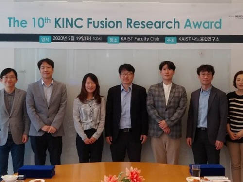 The 10th KINC Fusion Research Awardees
The KAIST Institute for NanoCentury (KINC) recognized three distinguished researchers whose convergence studies made significant impacts. The KINC presented the 10th KINC Fusion Research Awards during a ceremony that took place at KAIST’s main campus in Daejeon on May 19.
This year’s ‘best’ convergence research award went to a joint research group led by Professor Hee Tak Kim from the Department of Chemical and Biomolecular Engineering and Professor Sang Ouk Kim from the Department of Materials Science and Engineering. Their research, featured in the December 27 issue of Advanced Materials as a front cover article last year, introduced the world’s first high-energy efficiency, membraneless, flowless, zinc-bromine battery. This study, in which research professor Gyoung Hwa Jeong, postdoctoral researcher Yearin Byun, and PhD candidate Ju-Hyuck Lee took part as co-lead authors, is deemed as an example of a best practice in convergence research in which two groups’ respective expertise in the fields of carbon materials and electrochemical analysis created a synergistic effect.
Professor Bumjoon Kim from the Department of Chemical and Biomolecular Engineering was also recognized for having published the most interdisciplinary research papers on polymer electronics and nanomaterials at home and abroad.
Professor Hee-Tae Jung, the Director of KINC and the host of the KINC Fusion Research Awards, said, “The KINC is happy to announce the 10th awardees in nano-fusion research this year. Since convergence is crucial for making revolutionary changes, the importance of convergence studies should be recognized. Our institute will spare no effort to create a research environment suitable for convergence studies, which will be crucial for making a significant difference.”
The KINC was established in June 2006 under the KAIST Institute with the mission of facilitating convergence studies by tearing down boarders among departments and carrying out interdisciplinary joint research. Currently, the institute is comprised of approximately 90 professors from 13 departments. It aims to become a hub of university institutes for nano-fusion research.
(END)
2020.05.19 View 9159
The 10th KINC Fusion Research Awardees
The KAIST Institute for NanoCentury (KINC) recognized three distinguished researchers whose convergence studies made significant impacts. The KINC presented the 10th KINC Fusion Research Awards during a ceremony that took place at KAIST’s main campus in Daejeon on May 19.
This year’s ‘best’ convergence research award went to a joint research group led by Professor Hee Tak Kim from the Department of Chemical and Biomolecular Engineering and Professor Sang Ouk Kim from the Department of Materials Science and Engineering. Their research, featured in the December 27 issue of Advanced Materials as a front cover article last year, introduced the world’s first high-energy efficiency, membraneless, flowless, zinc-bromine battery. This study, in which research professor Gyoung Hwa Jeong, postdoctoral researcher Yearin Byun, and PhD candidate Ju-Hyuck Lee took part as co-lead authors, is deemed as an example of a best practice in convergence research in which two groups’ respective expertise in the fields of carbon materials and electrochemical analysis created a synergistic effect.
Professor Bumjoon Kim from the Department of Chemical and Biomolecular Engineering was also recognized for having published the most interdisciplinary research papers on polymer electronics and nanomaterials at home and abroad.
Professor Hee-Tae Jung, the Director of KINC and the host of the KINC Fusion Research Awards, said, “The KINC is happy to announce the 10th awardees in nano-fusion research this year. Since convergence is crucial for making revolutionary changes, the importance of convergence studies should be recognized. Our institute will spare no effort to create a research environment suitable for convergence studies, which will be crucial for making a significant difference.”
The KINC was established in June 2006 under the KAIST Institute with the mission of facilitating convergence studies by tearing down boarders among departments and carrying out interdisciplinary joint research. Currently, the institute is comprised of approximately 90 professors from 13 departments. It aims to become a hub of university institutes for nano-fusion research.
(END)
2020.05.19 View 9159 -
 A Theoretical Boost to Nano-Scale Devices
- Researchers calculate the quasi-Fermi levels in molecular junctions applying an initio approach. -
Semiconductor companies are struggling to develop devices that are mere nanometers in size, and much of the challenge lies in being able to more accurately describe the underlying physics at that nano-scale. But a new computational approach that has been in the works for a decade could break down these barriers.
Devices using semiconductors, from computers to solar cells, have enjoyed tremendous efficiency improvements in the last few decades. Famously, one of the co-founders of Intel, Gordon Moore, observed that the number of transistors in an integrated circuit doubles about every two years—and this ‘Moore’s law’ held true for some time.
In recent years, however, such gains have slowed as firms that attempt to engineer nano-scale transistors hit the limits of miniaturization at the atomic level.
Researchers with the School of Electrical Engineering at KAIST have developed a new approach to the underlying physics of semiconductors.
“With open quantum systems as the main research target of our lab, we were revisiting concepts that had been taken for granted and even appear in standard semiconductor physics textbooks such as the voltage drop in operating semiconductor devices,” said the lead researcher Professor Yong-Hoon Kim. “Questioning how all these concepts could be understood and possibly revised at the nano-scale, it was clear that there was something incomplete about our current understanding.”
“And as the semiconductor chips are being scaled down to the atomic level, coming up with a better theory to describe semiconductor devices has become an urgent task.”
The current understanding states that semiconductors are materials that act like half-way houses between conductors, like copper or steel, and insulators, like rubber or Styrofoam. They sometimes conduct electricity, but not always. This makes them a great material for intentionally controlling the flow of current, which in turn is useful for constructing the simple on/off switches—transistors—that are the foundation of memory and logic devices in computers.
In order to ‘switch on’ a semiconductor, a current or light source is applied, exciting an electron in an atom to jump from what is called a ‘valence band,’ which is filled with electrons, up to the ‘conduction band,’ which is originally unfilled or only partially filled with electrons. Electrons that have jumped up to the conduction band thanks to external stimuli and the remaining ‘holes’ are now able to move about and act as charge carriers to flow electric current.
The physical concept that describes the populations of the electrons in the conduction band and the holes in the valence band and the energy required to make this jump is formulated in terms of the so-called ‘Fermi level.’ For example, you need to know the Fermi levels of the electrons and holes in order to know what amount of energy you are going to get out of a solar cell, including losses.
But the Fermi level concept is only straightforwardly defined so long as a semiconductor device is at equilibrium—sitting on a shelf doing nothing—and the whole point of semiconductor devices is not to leave them on the shelf.
Some 70 years ago, William Shockley, the Nobel Prize-winning co-inventor of the transistor at the Bell Labs, came up with a bit of a theoretical fudge, the ‘quasi-Fermi level,’ or QFL, enabling rough prediction and measurement of the interaction between valence band holes and conduction band electrons, and this has worked pretty well until now.
“But when you are working at the scale of just a few nanometers, the methods to theoretically calculate or experimentally measure the splitting of QFLs were just not available,” said Professor Kim.
This means that at this scale, issues such as errors relating to voltage drop take on much greater significance.
Kim’s team worked for nearly ten years on developing a novel theoretical description of nano-scale quantum electron transport that can replace the standard method—and the software that allows them to put it to use. This involved the further development of a bit of math known as the Density Functional Theory that simplifies the equations describing the interactions of electrons, and which has been very useful in other fields such as high-throughput computational materials discovery.
For the first time, they were able to calculate the QFL splitting, offering a new understanding of the relationship between voltage drop and quantum electron transport in atomic scale devices.
In addition to looking into various interesting non-equilibrium quantum phenomena with their novel methodology, the team is now further developing their software into a computer-aided design tool to be used by semiconductor companies for developing and fabricating advanced semiconductor devices.
The study, featured at the Proceedings of the National Academy of Sciences of the USA on May 12, was supported by the National Research Foundation and the Korea Institute of Science and Technology Information Supercomputing Center.
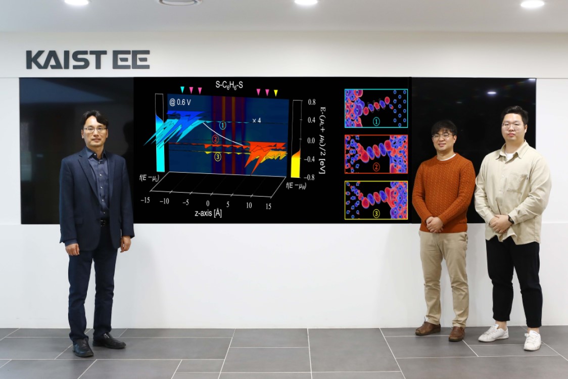
Image caption: The newly developed formalism and QFL splitting analysis led to new ways of characterizing extremely scaled-down semiconductor devices and the technology computer-aided design (TCAD) of next- generation nano-electronic/energy/bio devices.
Image credit: Yong-Hoon Kim, KAIST
Image usage restrictions: News organizations may use or redistribute this image, with proper attribution, as part of news coverage of this paper only.
Publication:
Juho Lee, Hyeonwoo Yeo, and Yong-Hoon Kim. (2020) ‘Quasi-Fermi level splitting in nanoscale junctions from ab initio.’ Proceedings of the National Academy of Sciences of the United States of America (PNAS), Volume 117, Issue 19, pp.10142-101488. Available online at https://doi.org/10.1073/pnas.1921273117
Profile:
Yong-Hoon Kim
Professor
y.h.kim@kaist.ac.kr
http://nanocore.kaist.ac.kr/
1st-Principles Nano-Device Computing Lab
School of Electrical Engineering
KAIST
(END)
2020.05.15 View 6019
A Theoretical Boost to Nano-Scale Devices
- Researchers calculate the quasi-Fermi levels in molecular junctions applying an initio approach. -
Semiconductor companies are struggling to develop devices that are mere nanometers in size, and much of the challenge lies in being able to more accurately describe the underlying physics at that nano-scale. But a new computational approach that has been in the works for a decade could break down these barriers.
Devices using semiconductors, from computers to solar cells, have enjoyed tremendous efficiency improvements in the last few decades. Famously, one of the co-founders of Intel, Gordon Moore, observed that the number of transistors in an integrated circuit doubles about every two years—and this ‘Moore’s law’ held true for some time.
In recent years, however, such gains have slowed as firms that attempt to engineer nano-scale transistors hit the limits of miniaturization at the atomic level.
Researchers with the School of Electrical Engineering at KAIST have developed a new approach to the underlying physics of semiconductors.
“With open quantum systems as the main research target of our lab, we were revisiting concepts that had been taken for granted and even appear in standard semiconductor physics textbooks such as the voltage drop in operating semiconductor devices,” said the lead researcher Professor Yong-Hoon Kim. “Questioning how all these concepts could be understood and possibly revised at the nano-scale, it was clear that there was something incomplete about our current understanding.”
“And as the semiconductor chips are being scaled down to the atomic level, coming up with a better theory to describe semiconductor devices has become an urgent task.”
The current understanding states that semiconductors are materials that act like half-way houses between conductors, like copper or steel, and insulators, like rubber or Styrofoam. They sometimes conduct electricity, but not always. This makes them a great material for intentionally controlling the flow of current, which in turn is useful for constructing the simple on/off switches—transistors—that are the foundation of memory and logic devices in computers.
In order to ‘switch on’ a semiconductor, a current or light source is applied, exciting an electron in an atom to jump from what is called a ‘valence band,’ which is filled with electrons, up to the ‘conduction band,’ which is originally unfilled or only partially filled with electrons. Electrons that have jumped up to the conduction band thanks to external stimuli and the remaining ‘holes’ are now able to move about and act as charge carriers to flow electric current.
The physical concept that describes the populations of the electrons in the conduction band and the holes in the valence band and the energy required to make this jump is formulated in terms of the so-called ‘Fermi level.’ For example, you need to know the Fermi levels of the electrons and holes in order to know what amount of energy you are going to get out of a solar cell, including losses.
But the Fermi level concept is only straightforwardly defined so long as a semiconductor device is at equilibrium—sitting on a shelf doing nothing—and the whole point of semiconductor devices is not to leave them on the shelf.
Some 70 years ago, William Shockley, the Nobel Prize-winning co-inventor of the transistor at the Bell Labs, came up with a bit of a theoretical fudge, the ‘quasi-Fermi level,’ or QFL, enabling rough prediction and measurement of the interaction between valence band holes and conduction band electrons, and this has worked pretty well until now.
“But when you are working at the scale of just a few nanometers, the methods to theoretically calculate or experimentally measure the splitting of QFLs were just not available,” said Professor Kim.
This means that at this scale, issues such as errors relating to voltage drop take on much greater significance.
Kim’s team worked for nearly ten years on developing a novel theoretical description of nano-scale quantum electron transport that can replace the standard method—and the software that allows them to put it to use. This involved the further development of a bit of math known as the Density Functional Theory that simplifies the equations describing the interactions of electrons, and which has been very useful in other fields such as high-throughput computational materials discovery.
For the first time, they were able to calculate the QFL splitting, offering a new understanding of the relationship between voltage drop and quantum electron transport in atomic scale devices.
In addition to looking into various interesting non-equilibrium quantum phenomena with their novel methodology, the team is now further developing their software into a computer-aided design tool to be used by semiconductor companies for developing and fabricating advanced semiconductor devices.
The study, featured at the Proceedings of the National Academy of Sciences of the USA on May 12, was supported by the National Research Foundation and the Korea Institute of Science and Technology Information Supercomputing Center.
Image caption: The newly developed formalism and QFL splitting analysis led to new ways of characterizing extremely scaled-down semiconductor devices and the technology computer-aided design (TCAD) of next- generation nano-electronic/energy/bio devices.
Image credit: Yong-Hoon Kim, KAIST
Image usage restrictions: News organizations may use or redistribute this image, with proper attribution, as part of news coverage of this paper only.
Publication:
Juho Lee, Hyeonwoo Yeo, and Yong-Hoon Kim. (2020) ‘Quasi-Fermi level splitting in nanoscale junctions from ab initio.’ Proceedings of the National Academy of Sciences of the United States of America (PNAS), Volume 117, Issue 19, pp.10142-101488. Available online at https://doi.org/10.1073/pnas.1921273117
Profile:
Yong-Hoon Kim
Professor
y.h.kim@kaist.ac.kr
http://nanocore.kaist.ac.kr/
1st-Principles Nano-Device Computing Lab
School of Electrical Engineering
KAIST
(END)
2020.05.15 View 6019 -
 Wearable Strain Sensor Using Light Transmittance Helps Measure Physical Signals Better
KAIST researchers have developed a novel wearable strain sensor based on the modulation of optical transmittance of a carbon nanotube (CNT)-embedded elastomer. The sensor is capable of sensitive, stable, and continuous measurement of physical signals. This technology, featured in the March 4th issue of ACS Applied Materials & Interfaces as a front cover article, shows great potential for the detection of subtle human motions and the real-time monitoring of body postures for healthcare applications.
A wearable strain sensor must have high sensitivity, flexibility, and stretchability, as well as low cost. Those used especially for health monitoring should also be tied to long-term solid performance, and be environmentally stable. Various stretchable strain sensors based on piezo-resistive and capacitive principles have been developed to meet all these requirements.
Conventional piezo-resistive strain sensors using functional nanomaterials, including CNTs as the most common example, have shown high sensitivity and great sensing performance. However, they suffer from poor long-term stability and linearity, as well as considerable signal hysteresis. As an alternative, piezo-capacitive strain sensors with better stability, lower hysteresis, and higher stretchability have been suggested. But due to the fact that piezo-capacitive strain sensors exhibit limited sensitivity and strong electromagnetic interference caused by the conductive objects in the surrounding environment, these conventional stretchable strain sensors are still facing limitations that are yet to be resolved.
A KAIST research team led by Professor Inkyu Park from the Department of Mechanical Engineering suggested that an optical-type stretchable strain sensor can be a good alternative to resolve the limitations of conventional piezo-resistive and piezo-capacitive strain sensors, because they have high stability and are less affected by environmental disturbances. The team then introduced an optical wearable strain sensor based on the light transmittance changes of a CNT-embedded elastomer, which further addresses the low sensitivity problem of conventional optical stretchable strain sensors.
In order to achieve a large dynamic range for the sensor, Professor Park and his researchers chose Ecoflex as an elastomeric substrate with good mechanical durability, flexibility, and attachability on human skin, and the new optical wearable strain sensor developed by the research group actually shows a wide dynamic range of 0 to 400%.
In addition, the researchers propagated the microcracks under tensile strain within the film of multi-walled CNTs embedded in the Ecoflex substrate, changing the optical transmittance of the film. By doing so, it was possible for them to develop a wearable strain sensor having a sensitivity 10 times higher than conventional optical stretchable strain sensors.
The proposed sensor has also passed the durability test with excellent results. The sensor’s response after 13,000 sets of cyclic loading was stable without any noticeable drift. This suggests that the sensor response can be used without degradation, even if the sensor is repeatedly used for a long time and in various environmental conditions.
Using the developed sensor, the research team could measure the finger bending motion and used it for robot control. They also developed a three-axes sensor array for body posture monitoring. The sensor was able to monitor human motions with small strains such as a pulse near the carotid artery and muscle movement around the mouth during pronunciation.
Professor Park said, “In this study, our group developed a new wearable strain sensor platform that overcomes many limitations of previously developed resistive, capacitive, and optical-type stretchable strain sensors. Our sensor could be widely used in a variety of fields including soft robotics, wearable electronics, electronic skin, healthcare, and even entertainment.”
This work was supported by the National Research Foundation (NRF) of Korea.
Publication:
Jimin Gu, Donguk Kwon, Junseong Ahn, and Inkyu Park. (2020) “Wearable Strain sensors Using Light Transmittance Change of Carbon Nanotube-Embedded Elastomers with Microcracks” ACS Applied Materials & Interfaces. Volume 12. Issue 9. Available online at https://doi.org/10.1021/acsami.9b18069
Profile:
Inkyu Park
Professor
inkyu@kaist.ac.kr
http://mintlab1.kaist.ac.kr
Micro/Nano Transducers Laboratory (MINT Lab)
Department of Mechanical Engineering (ME)Korea Advanced Institute of Science and Technology (KAIST)
Profile:
Jimin Gu
Ph.D. Candidate
mint9411@kaist.ac.kr
http://mintlab1.kaist.ac.kr
MINT Lab
KAIST ME
(END)
2020.03.20 View 12362
Wearable Strain Sensor Using Light Transmittance Helps Measure Physical Signals Better
KAIST researchers have developed a novel wearable strain sensor based on the modulation of optical transmittance of a carbon nanotube (CNT)-embedded elastomer. The sensor is capable of sensitive, stable, and continuous measurement of physical signals. This technology, featured in the March 4th issue of ACS Applied Materials & Interfaces as a front cover article, shows great potential for the detection of subtle human motions and the real-time monitoring of body postures for healthcare applications.
A wearable strain sensor must have high sensitivity, flexibility, and stretchability, as well as low cost. Those used especially for health monitoring should also be tied to long-term solid performance, and be environmentally stable. Various stretchable strain sensors based on piezo-resistive and capacitive principles have been developed to meet all these requirements.
Conventional piezo-resistive strain sensors using functional nanomaterials, including CNTs as the most common example, have shown high sensitivity and great sensing performance. However, they suffer from poor long-term stability and linearity, as well as considerable signal hysteresis. As an alternative, piezo-capacitive strain sensors with better stability, lower hysteresis, and higher stretchability have been suggested. But due to the fact that piezo-capacitive strain sensors exhibit limited sensitivity and strong electromagnetic interference caused by the conductive objects in the surrounding environment, these conventional stretchable strain sensors are still facing limitations that are yet to be resolved.
A KAIST research team led by Professor Inkyu Park from the Department of Mechanical Engineering suggested that an optical-type stretchable strain sensor can be a good alternative to resolve the limitations of conventional piezo-resistive and piezo-capacitive strain sensors, because they have high stability and are less affected by environmental disturbances. The team then introduced an optical wearable strain sensor based on the light transmittance changes of a CNT-embedded elastomer, which further addresses the low sensitivity problem of conventional optical stretchable strain sensors.
In order to achieve a large dynamic range for the sensor, Professor Park and his researchers chose Ecoflex as an elastomeric substrate with good mechanical durability, flexibility, and attachability on human skin, and the new optical wearable strain sensor developed by the research group actually shows a wide dynamic range of 0 to 400%.
In addition, the researchers propagated the microcracks under tensile strain within the film of multi-walled CNTs embedded in the Ecoflex substrate, changing the optical transmittance of the film. By doing so, it was possible for them to develop a wearable strain sensor having a sensitivity 10 times higher than conventional optical stretchable strain sensors.
The proposed sensor has also passed the durability test with excellent results. The sensor’s response after 13,000 sets of cyclic loading was stable without any noticeable drift. This suggests that the sensor response can be used without degradation, even if the sensor is repeatedly used for a long time and in various environmental conditions.
Using the developed sensor, the research team could measure the finger bending motion and used it for robot control. They also developed a three-axes sensor array for body posture monitoring. The sensor was able to monitor human motions with small strains such as a pulse near the carotid artery and muscle movement around the mouth during pronunciation.
Professor Park said, “In this study, our group developed a new wearable strain sensor platform that overcomes many limitations of previously developed resistive, capacitive, and optical-type stretchable strain sensors. Our sensor could be widely used in a variety of fields including soft robotics, wearable electronics, electronic skin, healthcare, and even entertainment.”
This work was supported by the National Research Foundation (NRF) of Korea.
Publication:
Jimin Gu, Donguk Kwon, Junseong Ahn, and Inkyu Park. (2020) “Wearable Strain sensors Using Light Transmittance Change of Carbon Nanotube-Embedded Elastomers with Microcracks” ACS Applied Materials & Interfaces. Volume 12. Issue 9. Available online at https://doi.org/10.1021/acsami.9b18069
Profile:
Inkyu Park
Professor
inkyu@kaist.ac.kr
http://mintlab1.kaist.ac.kr
Micro/Nano Transducers Laboratory (MINT Lab)
Department of Mechanical Engineering (ME)Korea Advanced Institute of Science and Technology (KAIST)
Profile:
Jimin Gu
Ph.D. Candidate
mint9411@kaist.ac.kr
http://mintlab1.kaist.ac.kr
MINT Lab
KAIST ME
(END)
2020.03.20 View 12362