%73%65%6d%69%63%6f%6e%64%75%63%74%6f%72%73
-
 KAIST Controls Where 2D Semiconductor Crystals Begin to Grow, Addressing a Key Challenge in Stacking AI Chips
Two-dimensional (2D) semiconductors, only a few atomic layers thick, are a promising material for making AI chips faster and more energy efficient by stacking additional semiconductor layers on top of existing computing circuits. However, when crystals form at multiple random locations during growth, it is difficult to produce high-quality semiconductors at the desired positions. A KAIST joint research team has developed a technology that sets in advance where a crystal begins to grow and allows only one crystal to grow at that position. By controlling the starting point of semiconductor growth, the work addresses a key challenge in realizing next-generation stacked semiconductors.
KAIST announced that a research team led by Professor Kibum Kang from the Department of Materials Science and Engineering, in collaboration with UNIST, Hanyang University, and TDS Innovation (Co-CEOs Kibum Kang and Sanghyun Mo), has developed a new growth technique that precisely controls the location of nucleation, the stage at which 2D semiconductor crystals first form, using chemical species released from an oxide barrier.
When AI generates responses or processes large amounts of data, time and power are consumed not only by computation but also by moving data within the chip. Stacking the devices used for computation and data storage vertically, so that they are placed close together, shortens the distance that data must travel and can reduce processing delays and power consumption. This requires a technology that forms high-quality semiconductors directly at the required positions on top of circuits that have already been fabricated.
Deposited semiconductors, in which devices are made by forming a thin film of semiconductor material directly on the required surface, are a promising technology for building stacked chips. 2D semiconductors are particularly well suited for stacking thin device layers because they retain the electrical properties of a semiconductor while being only a few atomic layers thick.
The challenge is that, as a thin semiconductor film grows, the positions where crystals begin to form are inherently random. A crystal is a structure in which the atoms that make up the semiconductor are arranged in a regular, repeating pattern. When crystals grow separately from several locations and meet, grain boundaries form between them. These boundaries hinder the movement of electrons and can degrade the quality of the semiconductor.
Area-selective growth techniques, which define in advance the regions where a semiconductor will grow, already existed. However, it has been difficult to control exactly where crystals first form within those regions and how many of them form. The research team achieved deterministic nucleation, in which nucleation that previously occurred at random takes place one at a time at defined positions. In addition to defining the region where the semiconductor will grow, the team also determined the point within that region where growth begins.
The researchers named the technique etching-flux-mediated single-centered nucleation (EF-SCN). The key element is oxygen released from an oxide barrier, such as hafnium oxide (HfO₂), that surrounds the growth region. This oxygen acts as an etching flux that suppresses the formation of crystal nuclei of molybdenum disulfide (MoS₂), a representative 2D semiconductor. Etching refers to chemically removing material, and flux refers to the flow of a specific chemical species that is transported and supplied in a way that affects nearby chemical reactions.
The suppressing effect is strong at the edges near the oxide barrier and becomes weaker toward the center, which is farthest from the barrier. Using this difference, the team caused a single crystal to begin growing at only one point in the center. While the crystal that started at the center continued to grow, the formation of new crystals around it was also suppressed, so that the single crystal could grow larger.
In experiments, the team grew one MoS₂ single crystal at a designated central position in more than 99% of 400 different patterns. A single crystal has one continuous atomic arrangement, and because it reduces the boundaries that form where multiple crystals meet, it is advantageous for producing high-quality semiconductors. Using MoS₂–MoSe₂ lateral heterostructures grown with this method, the team also deposited a thin film of ruthenium (Ru) metal selectively on the molybdenum diselenide (MoSe₂) regions only. The researchers further analyzed the principle behind this position control through growth experiments and simulations.
The significance of this work is that it turns the starting point of semiconductor thin-film growth, which had been determined at random, into a process parameter that can be designed. Instead of fabricating 2D semiconductors elsewhere and then transferring them, this approach could lead to a manufacturing technology that grows high-quality semiconductors directly at the required positions on a chip. Deposited semiconductors are expected to be adopted in the 2030s to improve the performance and lower the power consumption of AI chips. If applied to stacked AI chips, the technology could reduce the time and energy spent on moving data, which would shorten the time users wait for AI responses and reduce the power demands of data centers.
“In thin-film growth, where a crystal forms is inherently a matter of probability, and the key significance of this study is that it allows that starting point to be determined at a desired position,” said Professor Kibum Kang. Professor Kang added that the technology will serve as the basis for stacked-channel processes, in which semiconductor devices are stacked vertically, by growing high-quality 2D semiconductors directly where they are needed.
“In 2D semiconductors, the position where growth begins can change in response to even small chemical changes in the surroundings,” said Dr. Jeongwon Park, a co-first author. Park explained that the significance of the study lies in using this property to control where the semiconductor begins to grow.
Dr. Park and master’s student Jiyun Kim from the KAIST Department of Materials Science and Engineering, Sumin Kang, who received a master’s degree from the same department, integrated M.S.–Ph.D. student Jieun Oh from the Department of Materials Science and Chemical Engineering at Hanyang University, and integrated M.S.–Ph.D. student Youngmin Sunwoo from the Graduate School of Semiconductor Materials and Devices Engineering at UNIST participated as co-first authors. The findings were published in Nature on October 8.
Paper title: Spatially deterministic nucleation of 2D semiconductors by etching flux
DOI: 10.1038/s41586-026-11095-1
This research was supported by the Nano and Material Technology Development Program and the Basic Science Research Program of the National Research Foundation of Korea (NRF), funded by the Ministry of Science and ICT (MSIT). Additional support was provided by the International Cooperation Program for Source Technology Development, the Development of vdW Materials and Process Technologies for Ultra-High-Density Semiconductors Program, the Next-Generation Intelligent Semiconductor Technology Development Program, the Ministry of Trade, Industry and Energy (MOTIE), the Korea Institute for Advancement of Technology (KIAT), the Commercialization Promotion Agency for R&D Outcomes (COMPA), the Innopolis Foundation, the Ministry of SMEs and Startups (MSS), and NVIDIA.
2026.10.13 View 105
-
 KAIST Develops AI Chip That Recognizes Changes in Motion over Time
For a wearable device to distinguish walking from a brief swing of the arm, it must recognize how a movement changes over time. Korean researchers have developed a technology that stacks semiconductor devices with different response speeds, allowing them to recognize both a change that has just occurred and the changes before it. The technology could be applied to small devices that are worn on or attached to the body to analyze movement and physiological signals.
KAIST (President Choongsik Bae) announced on September 29 that a research team led by Professor Jimin Kwon from the Department of AI Systems, together with researchers from UNIST (President Chong Rae Park) and POSTECH (President Seong Keun Kim), has made a solid thin film from a material that contains ions and used it to stack semiconductor devices with different response speeds in multiple layers.
In these devices, applying a voltage moves the ions within the material and changes the flow of current. When the voltage is removed, the ions require time to return to their original state. As a result, the effect of previous signals remains in the device for a short time. This slow movement has generally been considered a disadvantage, but the research team used it to identify earlier inputs.
The main challenge was controlling how long this effect lasts. Until now, such materials have mostly been liquids or soft gels, which made it difficult to fabricate the devices precisely or to stack them in multiple layers.
To address this challenge, the team made the material into a solid thin film, known as a solid-state ionogel, and adjusted the amount of ions in the film as well as its thickness. This allowed them to create devices that respond to signals either quickly or slowly. When the two types were stacked, one layer responded to the most recent signal, while the other responded to signals that had accumulated over a longer period.
The researchers confirmed that the devices could distinguish all 16 patterns created when four consecutive input signals are turned on or off in different combinations. Using the responses measured from the devices, they also built a simulation model of a system that classifies videos of moving handwritten digits. The model achieved validation accuracies above 90% for sequences of moving images played at different speeds.
The team fabricated the devices on both 4-inch wafers and flexible substrates. Their electrical characteristics remained stable for 55 months after fabrication.
The results could be used to develop technologies for processing information that changes over time, such as movement and signals from the body, directly on small devices. Further validation is needed to determine how the technology performs, and how much power it saves, in actual smartwatches.
"These devices can be fabricated on large-area substrates using existing thin-film semiconductor processes, and they can also be stacked in multiple layers," said Professor Kwon. He added that the technology could be developed into AI chips that analyze movement and physiological signals for devices that must operate with low power consumption, such as smartwatches.
Research Professor Haksoon Jung from KAIST is the first author of the study, and Professor Yong-Young Noh of POSTECH and Professor Jimin Kwon of KAIST are the co-corresponding authors. The findings were published in Advanced Materials on June 30.
Paper title: Monolithic 3D-Integrated All-Solid Ion-Gated Carbon Nanotube Transistors With Tunable Ionic Conductance for Multi-Timescale Reservoir Computing,
DOI: 10.1002/adma.202523703
This research was supported by the National R&D Program through the National Research Foundation of Korea (NRF), funded by the Korean government (Ministry of Science and ICT, MSIT) (RS-2023-00281195 and RS-2024-00355384), and by the Korea Planning & Evaluation Institute of Industrial Technology (KEIT), funded by the Ministry of Trade, Industry & Energy (MOTIE, Korea) (RS-2024-00417909).
2026.09.29 View 994
-
 KAIST Extends Lifespan of Graphite-Free Anode-Free Batteries That Could Make EV Batteries Smaller and Lighter
Korean researchers have developed a technology that could make electric-vehicle (EV) batteries smaller and lighter while helping EVs travel farther on a single charge. A KAIST research team has proposed a new solution to a persistent problem in anode-free batteries, which reduce weight and volume by eliminating anode materials such as graphite that normally store lithium during charging. In these batteries, lithium can grow into sharp, spike-like structures that shorten battery life. The key lies in using nanofabrication techniques employed in semiconductor manufacturing to create uniform sites for lithium deposition and promote the formation of a robust protective layer.
KAIST (President Choongsik Bae) announced on September 22 that a joint research team led by Professors Jinwoo Lee and Hee-Tae Jung from the Department of Chemical and Biomolecular Engineering, working with researchers from Kyungpook National University (President Heo Young-woo) and the National NanoFab Center (President Park Heung Soo), has developed a new technology that extends the lifespan of anode-free batteries by applying the ultrafine fabrication processes used in semiconductor device manufacturing to batteries.
Conventional lithium-ion batteries store lithium in an anode material such as graphite during charging. Anode-free batteries, by contrast, deposit lithium directly onto a thin copper foil without a separate anode material. Because they eliminate the weight and volume that the anode material would otherwise occupy, they are drawing attention as a next-generation technology capable of packing more energy into a battery of the same size.
However, repeated charging and discharging cause lithium to deposit unevenly on the copper foil, growing into branch- or spike-like structures known as dendrites. The protective layer over the lithium also becomes unstable, causing the battery’s performance and lifespan to deteriorate rapidly. This is one of the most significant obstacles standing in the way of commercializing anode-free batteries.
Some previous approaches to extending the lifespan of anode-free batteries involved adding excess lithium or applying a thick protective layer to the surface. These methods provide extra lithium to compensate for losses during use or coat the surface with a protective film. However, adding more material makes the battery heavier and thicker, undercutting the very advantage of a small, lightweight anode-free battery.
To minimize added weight and volume, the research team modified the copper foil on which lithium is deposited. Much like marking out closely spaced parking bays in a flat lot, the team created an array of microscopic tube-shaped structures on the copper surface so that lithium spreads out and deposits evenly rather than concentrating in one spot.
To do this, the team used a process called secondary sputtering lithography (SSL), used for the precise micromachining of semiconductors. Fabricating microscopic tubes about 300 nanometers in diameter and 150 nanometers in height on the copper foil increased the surface area available for lithium deposition to about four times that of flat copper foil, helping to reduce localized, spike-like lithium growth.
The team then coated the copper foil with a roughly 10-nanometer-thick layer of MXene, a two-dimensional material, forming an ultrathin film only a few thousandths the thickness of a human hair. Rather than serving as a finished protective layer itself, the MXene acts like a primer that draws together the components needed to form one. In the LiPF6-based electrolyte used in the study, the MXene surface promotes the formation of a robust protective layer rich in lithium fluoride (LiF) as the battery operates.
This protective layer reduces unwanted reactions between the lithium and the electrolyte and also suppresses the spike-like growth of lithium. By examining electrode surfaces and cross sections while minimizing air exposure, the research team confirmed that a nanoscale protective layer forms uniformly along the MXene and identified the mechanism behind its formation. The analysis employed X-ray photoelectron spectroscopy (XPS), time-of-flight secondary ion mass spectrometry (ToF-SIMS), and transmission electron microscopy (TEM), among other techniques.
Professor Jinwoo Lee said, “This study shows how ultrafine fabrication techniques used in semiconductor manufacturing can create both uniform sites for lithium deposition and a stable protective layer without changing the bulk electrolyte formulation or adding excess lithium.” He added that the technology is expected to serve as a foundation for accelerating the commercialization of high-energy anode-free batteries by extending battery life while minimizing increases in weight and volume.
KAIST researchers Eunji Kim, Hyunju Jung, and Jinuk Kim participated as co-first authors on the study. The findings were published online in the international journal Advanced Functional Materials on September 1.
Paper title: Anion-Interactive Anode Interfaces for Stable Anode-Free Lithium Metal Batteries,
DOI 10.1002/adfm.77931
Author information: Eunji Kim (KAIST/National NanoFab Center, co-first author), Hyunju Jung (KAIST, co-first author), Jinuk Kim (KAIST, co-first author), Hee-Tae Jung (KAIST, corresponding author), Yonghee Lee (Kyungpook National University, corresponding author), Jinwoo Lee (KAIST, corresponding author)
This research was supported by the Nano&Material Technology Development Program through the National Research Foundation of Korea (NRF) funded by Ministry of Science and ICT (RS-2026-25542167), as well as the Global Semiconductor Advanced Fab Utilization Project through the National Nano Fab Center (NNFC). This work was also supported by Semiconductor-Secondary Battery Interfacing Platform Technology Development Project of NNFC.
2026.09.22 View 2850
-
 Single Material Enables Efficient Charge Injection into Two Types of Ultrathin Semiconductors, Paving the Way for Smaller, More Energy-Efficient AI Chips
A new approach could help make future AI chips smaller and more energy-efficient. A KAIST-led research team has used a single material to address one of the major obstacles facing atomically thin semiconductors, the difficulty of efficiently injecting charge. The technology could contribute to next-generation AI and low-power semiconductor devices in which multiple ultrathin layers are vertically integrated to increase device density and performance.
KAIST (President Choongsik Bae) announced on September 16 that a research team led by Professor Joonki Suh from the Department of Chemical and Biomolecular Engineering has developed a ‘universal van der Waals tunneling injector’ based on tin diselenide (SnSe2). The single-material injector efficiently supplies charge to two different types of atomically thin semiconductor channels.
The study was conducted in collaboration with researchers from Yonsei University, the Beijing Computational Science Research Center in China, the Korea Institute of Science and Technology (KIST), Hanyang University, the Ulsan National Institute of Science and Technology (UNIST), and Samsung Electronics.
A transistor is a microscopic switch that controls the flow of electric current. Nearly every semiconductor chip, from those used in smartphones and computers to advanced AI processors, contains vast numbers of transistors.
Transistors can be broadly classified as n-type or p-type. In n-type transistors, ‘electrons’ carry the current, while in p-type transistors, current is carried by ‘holes’, which are empty electron states that act as positive charge carriers. Modern semiconductor chips combine these two types in complementary metal-oxide-semiconductor, or CMOS, circuits, which enable fast operation while minimizing power consumption.
Two-dimensional semiconductors, which can be less than a nanometer thick, have recently emerged as promising materials for making chips smaller and more energy-efficient. Their atomically thin structure also makes it possible to stack multiple device layers vertically, potentially allowing more transistors to be integrated within the same footprint.
A persistent challenge, however, has been injecting charge efficiently into such ultrathin semiconductors. Depositing a conventional metal electrode directly onto a two-dimensional semiconductor can damage its delicate atomic structure during fabrication. The resulting interface can also create an energy barrier that obstructs the injection of electrons or holes.
In atomically thin semiconductors, the ‘entry point’ for electrical charge has been a major bottleneck limiting transistor performance. Complicating matters further, n-type and p-type channels generally require different contact conditions and have therefore relied on separately optimized electrodes.
The research team addressed this problem using a single material: tin diselenide (SnSe2), a layered semiconductor composed of tin (Sn) and selenium (Se). Instead of forming strong chemical bonds with the semiconductor channel, SnSe2 can be placed in contact with it through weak interatomic attractions known as van der Waals forces. This approach preserves the atomically thin channel and creates a clean, uniform interface.
Crucially, SnSe2 provides a different but favorable charge-injection pathway depending on the semiconductor with which it is paired.
When combined with p-type tungsten diselenide (WSe2), SnSe2 forms a type-III, or ‘broken-gap’, band alignment that enables efficient band-to-band tunneling. In this process, charge carriers pass through an energy barrier quantum mechanically rather than having to acquire enough energy to travel over it. When combined with n-type molybdenum disulfide (MoS2), the same SnSe2 injector forms a different junction. An applied gate field reshapes and narrows the electron-injection barrier, allowing electrons to tunnel through it.
In other words, whereas n-type and p-type transistors previously required separately optimized charge-injection contacts, SnSe2 serves as a single, shared injector that adapts to both channel polarities through different tunneling mechanisms.
The resulting performance improvements were substantial. In p-type WSe2 transistors, the SnSe2 injector increased the maximum drive current by more than 1,000 times compared with conventional nickel electrodes. Drive current refers to the maximum current that a transistor can deliver when switched on.
In n-type MoS₂ transistors, the SnSe2 injector enabled steep switching and an on/off current ratio exceeding one billion (109). This means that the device conducts current effectively in its on state while strongly suppressing current in its off state.
The team also fabricated a CMOS inverter, a basic building block of digital circuits that combines n-type and p-type transistors, and confirmed that it operated reliably in response to repeated input signals.
The key contribution of this research is that it demonstrated a single material can efficiently supply charge to both types of ultrathin semiconductors, moving beyond the conventional approach of using separate electrodes for n-type and p-type devices.
With further advances in direct growth, large-area fabrication, and device integration, two-dimensional semiconductors could eventually be stacked in multiple layers to form three-dimensional chips. Such architectures could accommodate more transistors within the same footprint and perform more functions while consuming less power, contributing to the development of next-generation AI processors and ultra-low-power electronic devices.
“This study demonstrates that efficient charge injection, one of the most challenging bottlenecks in monolayer two-dimensional semiconductors, can be addressed using a single material platform,” said Professor Joonki Suh. “With further advances in direct growth and large-area processing technologies, this approach could accelerate the practical implementation of low-power two-dimensional CMOS integrated circuits.”
The study was led by KAIST PhD candidate Hanbin Cho as first author, with Professor Kyungmin Ko from Yonsei University and Professor Joonki Suh from KAIST serving as co-corresponding authors. The paper was published online on August 12 in the international journal Advanced Materials.
Paper title: “A Universal van der Waals Tunneling Injector for Monolayer CMOS”
DOI: 10.1002/adma.74597Authors: Hanbin Cho of KAIST, first author; Professor Kyungmin Ko of Yonsei University and Professor Joonki Suh of KAIST, co-corresponding authors
This work was primarily supported by Samsung Electronics Co., Ltd. It also received support from Korean funding agencies, including the National Research Foundation of Korea (NRF), funded by the Ministry of Science and ICT and the Ministry of Education.
2026.09.16 View 2528
-
 KAIST Solves 3D Memory Reliability Problem with "Oxygen Tunnel" Structure, Boosting AI Chip Performance and Reducing Power Consumption
As AI systems become more advanced, memory is required to transfer larger amounts of data at higher speeds. But conventional planar semiconductor scaling is running out of room. A KAIST research team has now addressed a key weakness in three-dimensional, vertically stacked memory devices, opening a new path to faster, more power-efficient AI semiconductors.
KAIST (President Choongsik Bae) announced on August 25 that a research team led by Professor Jimin Kwon from the School of Electrical Engineering has developed a new multilayer interlayer dielectric structure that reduces defects and significantly enhances the performance of oxide vertical channel transistors (VCTs), a next-generation memory device. The study was conducted in collaboration with researchers from UNIST, Yonsei University, and other Korean institutions.
DRAM, which serves as the main memory in computers, has advanced over the past several decades by scaling down device size while reducing power leakage. More recently, vertical channel structures, in which current flows vertically, have become a key technology for increasing memory density.
The challenge is oxygen vacancies — defects caused by the absence of oxygen atoms in the oxide semiconductor — which destabilizes the material's electrical properties. But oxygen cannot simply be supplied without limit: when oxygen is supplied to suppress oxygen vacancies, some of the oxygen tends to migrate further, reaching the metal electrode and oxidizing it, which degrades device performance instead. The channel needed oxygen; the electrode did not. Therefore, selectively controlling oxygen flow became a key challenge.
The KAIST team developed a new multilayer interlayer dielectric consisting of silicon nitride/silicon dioxide/silicon nitride (SiN/SiO₂/SiN), engineered to function as an "oxygen tunnel" that steers oxygen selectively toward the channel while blocking its path to the electrode. The structure enabled stable compensation of oxygen vacancies in the oxide semiconductor while simultaneously suppressing unwanted oxidation at the electrode, thereby resolving the trade-off.
As a result, the researchers achieved world-class current density and data retention time in oxide vertical channel transistors.
The device also demonstrated outstanding operational stability. Even after more than ten million cycles of harsh electrical stress testing, the threshold voltage shift remained below 50 millivolts (mV), confirming its high reliability as a memory device.
The team further evaluated system-level performance by integrating conventional silicon CMOS technology with the new oxide semiconductor platform. The results suggest that this approach could significantly improve the performance of next-generation compute-in-memory (CIM) systems, intelligent semiconductors that perform AI computation directly inside memory.
Hyeonho Gu, the first author of the study, said, “This research is significant because it goes beyond improving memory density and addresses the long-standing instability problem in 3D devices through a new approach based on oxygen migration control.” He added, “We expect this technology to play a key role in accelerating the commercialization of ultra-low-power, high-performance compute-in-memory systems required for the AI era.”
This study was led by KAIST researcher Hyeonho Gu as the first author and was published on May 20 in Advanced Functional Materials, a leading international journal in materials science. The paper was also selected as a Front Cover article in recognition of its academic significance and originality.
Paper title: Oxygen-Tunnel Indium Tin Oxide Vertical Channel Transistors with Enhanced Current Density and Reliability for Monolithic 3D Compute-In-Memory Systems
DOI: https://doi.org/10.1002/adfm.202531989
Author information: Hyeonho Gu (KAIST, first author); Yongwoo Lee (KAIST, corresponding author); Haksoon Jung (KAIST, corresponding author); Jimin Kwon (KAIST, corresponding author); Hoichang Jeong (UNIST, co-author); Yanfeng Zhao (UNIST, co-author); Heesoo Yang (UNIST, co-author); Minho Park (UNIST, co-author); Hyeonjin Lee (UNIST, co-author); Seunghun Baek (UNIST, co-author); Minju Song (UNIST, co-author); Junghwan Kim (UNIST, co-author); Youngmin Jo (KAIST, co-author); Hyunjin Park (Korea Research Institute of Chemical Technology, co-author); Munhyeon Kim (Seoul National University of Science and Technology, co-author); Jae-Joon Kim (Seoul National University, co-author); Kyuho Jason Lee (Yonsei University, co-author); and Byungjo Kim (UNIST, co-author).
This research was supported by the National Semiconductor Laboratory Program and the Excellent Young Researcher Program of the National Research Foundation of Korea, funded by the Ministry of Science and ICT; the Broadcast and Telecommunications Industry Technology Development Program of the Institute of Information & Communications Technology Planning & Evaluation; and the Super Gap Technology Development Program of the Korea Evaluation Institute of Industrial Technology, funded by the Ministry of Trade, Industry and Energy.
2026.08.20 View 2657
-
 KAIST Finds Clue to Solving the “Electrical Bottleneck” in Semiconductors
When the pathways through which electricity flows inside a semiconductor become blocked, device performance declines and power loss increases. A Korean research team has developed a new structure that could resolve this “electrical bottleneck” and, for the first time, directly confirmed that electric charges flow continuously without interruption. This achievement is expected to become a key technology for improving the performance and power efficiency of future semiconductors, including AI semiconductors and ultra-low-power semiconductors.
KAIST announced on July 13 that a research team led by Professor Seungbum Hong from the Department of Materials Science and Engineering, in collaboration with Professor Kibum Kang from the Department of Materials Science and Engineering at KAIST and Professor Sung Beom Cho’s research team at Sungkyunkwan University, has realized a new structure in which electricity flows without obstruction in a two-dimensional material—an ultrathin material only one or two atomic layers thick—that is attracting attention for next-generation semiconductor devices. The team also developed an analytical platform capable of directly observing this charge transport at the nanometer scale.
In semiconductors, contact resistance, which arises at the interface where a metal electrode meets a semiconductor, degrades performance and causes power loss. Especially as semiconductors continue to scale down, the influence of contact resistance becomes even greater, making it one of the most challenging technical bottlenecks in developing next-generation semiconductors.
Instead of attaching a metal electrode on top of a semiconductor as in conventional approaches, the research team continuously formed semi-metallic and semiconducting regions within a single two-dimensional m
aterial. By creating a structure in which the two regions are naturally connected within the same material, the team demonstrated for the first time that current can flow across the boundary without being blocked.
Specifically, the team continuously implemented a semi-metallic region and a semiconducting region within a single thin film of platinum diselenide (PtSe₂), an atomically thin two-dimensional material. By realizing a monolithic structure, in which a single material is formed continuously without interruption, the team proposed a new structure that allows current to flow across the boundary without obstruction.
Using Atomic Force Microscopy (AFM), a microscope that uses a probe to measure surface and electrical properties down to the atomic level, the team directly visualized charge transport inside the thin film at the nanometer scale.
As a result, the team confirmed for the first time that, when current moved from the semi-metallic region to the semiconducting region, the flow continued naturally without an “electrical bottleneck,” such as a blockage or bending of the current path. This is the first experimental demonstration that a monolithic interface does not interfere with current flow.
Furthermore, the team verified device operation by applying an electric field to the semiconducting region. The results confirmed that current flow can be stably controlled in a metal–semiconductor junction structure, demonstrating the potential of the structure for next-generation electronic devices.
This study presents a source technology that can dramatically reduce contact resistance in next-generation semiconductor devices based on two-dimensional materials. It is expected to be widely applicable to the development of future semiconductor technologies, including AI semiconductors, ultra-low-power semiconductors, and next-generation logic semiconductors.
The study was co-first-authored by Yeongyu Kim, a Ph.D. candidate and Dr. Minseung Gyeon from the Department of Materials Science and Engineering at KAIST; and Ji Hoon Hong, a Ph.D. candidate at Sungkyunkwan University. The work was published in the July 2026 issue of Matter, an international journal in the field of materials science.
※ Paper title: Nanoscale imaging of charge transport across the semimetal-semiconductor interface in monolithic platinum diselenide
DOI:https://doi.org/10.1016/j.matt.2026.102873
This research was supported by the STEAM Research Program and the Nanomaterials Technology Development Program of the Ministry of Science and ICT and the National Research Foundation of Korea.
2026.07.13 View 2054
-
 KAIST Automates the Search for “Dream Semiconductor” 2D Semiconductors
The era of researchers manually searching for two-dimensional semiconductors, which are drawing attention as next-generation AI semiconductors, is coming to an end. KAIST researchers have automated semiconductor screening and device fabrication, analyzed thousands of devices, and revealed the relationship between thickness and performance that had long been difficult to identify. This achievement is expected to shift next-generation semiconductor research toward a data-driven approach and accelerate the commercialization of AI semiconductors and ultra-low-power semiconductors.
KAIST (President Choongsik Bae) announced on the 9th that a research team led by Professor Jimin Kwon of the School of Electrical Engineering and the Department of AI System has developed a technology that automatically identifies two-dimensional semiconductors from optical microscope images alone and connects the process to transistor fabrication, through joint research with UNIST, Hanbat National University, Hanyang University, and Washington University in St. Louis in the United States.
Two-dimensional semiconductors are ultrathin semiconductors only a few atomic layers thick. They are called “dream semiconductors” because they can enable smaller semiconductors that consume less electricity than conventional silicon semiconductors. Today’s silicon semiconductors are approaching physical limits, as continued miniaturization of circuits leads to greater power loss and heat generation. Two-dimensional semiconductors, which are attracting attention as next-generation materials to overcome these limits, are expected to be used in a wide range of future technologies, including AI semiconductors, smartphones, data centers, wearable devices, foldable or stretchable electronics, and ultra-small medical sensors.
However, in two-dimensional semiconductors made through solution processing, the position, size, and thickness of each small semiconductor flake all differ, requiring researchers to find the desired samples one by one under a microscope. They then had to manually design electrodes according to the identified positions, requiring substantial time and effort, and making it practically difficult to analyze thousands or more devices at once.
The research team used molybdenum disulfide (MoS₂), a representative two-dimensional semiconductor material. By using the fact that the RGB red, green, and blue brightness values seen under a microscope change depending on thickness, the team enabled a computer to automatically identify the desired semiconductor and automatically design the electrodes. Verification using atomic force microscopy (AFM) confirmed that even subtle thickness differences of three to eight layers could be accurately distinguished.
Through this approach, the team successfully selected suitable samples automatically from more than 120,000 semiconductor flakes and fabricated and analyzed 1,615 transistors.
The large-scale analysis also produced meaningful results. The team statistically clarified for the first time that as the semiconductor becomes thicker, current flows more easily, but the ability to switch electricity on and off actually decreases. This characteristic had been difficult to confirm previously because only a small number of samples could be analyzed, but the team revealed it through large-scale data.
The greatest significance of this study is that it did not simply automate the fabrication process, but transformed two-dimensional semiconductor research, which had relied on human experience, into data-driven research. Going forward, the technology is expected to enable researchers to fabricate and analyze more semiconductors more quickly, identify high-performance materials, and ultimately expand into research in which AI designs new semiconductors.
This study was conducted with Professor Jimin Kwon, Dr. Haksoon Jung, and Dr. Yongwoo Lee of KAIST as co-corresponding authors, and Sanghyun Lee of UNIST as the first author. The research results were published on April 3 in Advanced Functional Materials, a leading international journal in materials science, and were also selected as an Inside Back Cover article in the field of 2D Materials & Electronics.
※ Paper title: Statistically Resolving Thickness-Dependent Electrical Characteristics in Multilayer-MoS₂ Transistors, DOI: 10.1002/adfm.202532204
※ Author information: Professor Jimin Kwon (KAIST, corresponding author), Dr. Haksoon Jung (KAIST, corresponding author), Dr. Yongwoo Lee (KAIST, corresponding author), Sanghyun Lee (UNIST, first author), and participating researchers from partner institutions: Sumin Hong (UNIST), Minho Park (UNIST), Professor Seongju Kim (Hanbat National University), Professor Sang-Hoon Baek (Hanyang University), Professor Joonki Suh (KAIST), Seonguk Yang (KAIST), Professor Sang-Hoon Bae (Washington University in St. Louis), and Dr. Chang-Soo Lee (TDS)
This research was supported by the Individual Basic Research Program of the National Research Foundation of Korea (NRF), funded by the Ministry of Science and ICT (MSIT), and by the Advanced Strategic Industry Super-Gap Technology Development Program of the Korea Planning & Evaluation Institute of Industrial Technology (KEIT), funded by the Ministry of Trade, Industry and Energy (MOTIE).
2026.07.09 View 3881
-
 KAIST Turns an Unprecedented Idea into Reality: Quantum Computing with Magnets
What started as an idea under KAIST’s Global Singularity Research Project—"Can we build a quantum computer using magnets?"—has now become a scientific reality. A KAIST-led international research team has successfully demonstrated a core quantum computing technology using magnetic materials (ferromagnets) for the first time in the world.
KAIST (represented by President Kwang-Hyung Lee) announced on the 6th of May that a team led by Professor Kab-Jin Kim from the Department of Physics, in collaboration with the Argonne National Laboratory and the University of Illinois Urbana-Champaign (UIUC), has developed a “photon-magnon hybrid chip” and successfully implemented real-time, multi-pulse interference using magnetic materials—marking a global first.
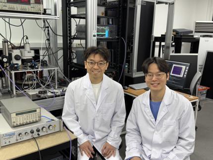
< Photo 1. Dr. Moojune Song (left) and Professor Kab-Jin Kim (right) of KAIST Department of Physics >
In simple terms, the researchers developed a special chip that synchronizes light and internal magnetic vibrations (magnons), enabling the transmission of phase information between distant magnets. They succeeded in observing and controlling interference between multiple signals in real time. This marks the first experimental evidence that magnets can serve as key components in quantum computing, serving as a pivotal step toward magnet-based quantum platforms.
The N and S poles of a magnet stem from the spin of electrons inside atoms. When many atoms align, their collective spin vibrations create a quantum particle known as a “magnon.”
Magnons are especially promising because of their nonreciprocal nature—they can carry information in only one direction, which makes them suitable for quantum noise isolation in compact quantum chips. They can also couple with both light and microwaves, enabling the potential for long-distance quantum communication over tens of kilometers.
Moreover, using special materials like antiferromagnets could allow quantum computers to operate at terahertz (THz) frequencies, far surpassing today’s hardware limitations, and possibly enabling room-temperature quantum computing without the need for bulky cryogenic equipment.
To build such a system, however, one must be able to transmit, measure, and control the phase information of magnons—the starting point and propagation of their waveforms—in real time. This had not been achieved until now.
< Figure 1. Superconducting Circuit-Based Magnon-Photon Hybrid System. (a) Schematic diagram of the device. A NbN superconducting resonator circuit fabricated on a silicon substrate is coupled with spherical YIG magnets (250 μm diameter), and magnons are generated and measured in real-time via a vertical antenna. (b) Photograph of the actual device. The distance between the two YIG spheres is 12 mm, a distance at which they cannot influence each other without the superconducting circuit. >
Professor Kim’s team used two tiny magnetic spheres made of Yttrium Iron Garnet (YIG) placed 12 mm apart with a superconducting resonator in between—similar to those used in quantum processors by Google and IBM. They input pulses into one magnet and successfully observed lossless transmission of magnon vibrations to the second magnet via the superconducting circuit.
They confirmed that from single nanosecond pulses to four microwave pulses, the magnon vibrations maintained their phase information and demonstrated predictable constructive or destructive interference in real time—known as coherent interference.
By adjusting the pulse frequencies and their intervals, the researchers could also freely control the interference patterns of magnons, effectively showing for the first time that electrical signals can be used to manipulate magnonic quantum states.
This work demonstrated that quantum gate operations using multiple pulses—a fundamental technique in quantum information processing—can be implemented using a hybrid system of magnetic materials and superconducting circuits. This opens the door for the practical use of magnet-based quantum devices.
< Figure 2. Experimental Data. (a) Measurement results of magnon-magnon band anticrossing via continuous wave measurement, showing the formation of a strong coupling hybrid system. (b) Magnon pulse exchange oscillation phenomenon between YIG spheres upon single pulse application. It can be seen that magnon information is coherently transmitted at regular time intervals through the superconducting circuit. (c,d) Magnon interference phenomenon upon dual pulse application. The magnon information state can be arbitrarily controlled by adjusting the time interval and carrier frequency between pulses. >
Professor Kab-Jin Kim stated, “This project began with a bold, even unconventional idea proposed to the Global Singularity Research Program: ‘What if we could build a quantum computer with magnets?’ The journey has been fascinating, and this study not only opens a new field of quantum spintronics, but also marks a turning point in developing high-efficiency quantum information processing devices.”
The research was co-led by postdoctoral researcher Moojune Song (KAIST), Dr. Yi Li and Dr. Valentine Novosad from Argonne National Lab, and Prof. Axel Hoffmann’s team at UIUC. The results were published in Nature Communications on April 17 and npj Spintronics on April 1, 2025.
Paper 1: Single-shot magnon interference in a magnon-superconducting-resonator hybrid circuit, Nat. Commun. 16, 3649 (2025)
DOI: https://doi.org/10.1038/s41467-025-58482-2
Paper 2: Single-shot electrical detection of short-wavelength magnon pulse transmission in a magnonic ultra-thin-film waveguide, npj Spintronics 3, 12 (2025)
DOI: https://doi.org/10.1038/s44306-025-00072-5
The research was supported by KAIST’s Global Singularity Research Initiative, the National Research Foundation of Korea (including the Mid-Career Researcher, Leading Research Center, and Quantum Information Science Human Resource Development programs), and the U.S. Department of Energy.
2025.06.12 View 18668
-
 ‘Carrier-Resolved Photo-Hall’ to Push Semiconductor Advances
(Professor Shin and Dr. Gunawan (left))
An IBM-KAIST research team described a breakthrough in a 140-year-old mystery in physics. The research reported in Nature last month unlocks the physical characteristics of semiconductors in much greater detail and aids in the development of new and improved semiconductor materials.
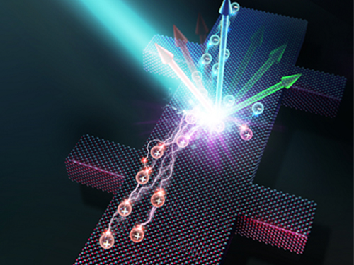
Research team under Professor Byungha Shin at the Department of Material Sciences and Engineering and Dr. Oki Gunawan at IBM discovered a new formula and technique that enables the simultaneous extraction of both majority and minority carrier information such as their density and mobility, as well as gain additional insights about carrier lifetimes, diffusion lengths, and the recombination process. This new discovery and technology will help push semiconductor advances in both existing and emerging technologies.
Semiconductors are the basic building blocks of today’s digital electronics age, providing us with a multitude of devices that benefit our modern life. To truly appreciate the physics of semiconductors, it is very important to understand the fundamental properties of the charge carriers inside the materials, whether those particles are positive or negative, their speed under an applied electric field, and how densely they are packed into the material.
Physicist Edwin Hall found a way to determine those properties in 1879, when he discovered that a magnetic field will deflect the movement of electronic charges inside a conductor and that the amount of deflection can be measured as a voltage perpendicular to the flow of the charge. Decades after Hall’s discovery, researchers also recognized that they can measure the Hall effect with light via “photo-Hall experiments”. During such experiments, the light generates multiple carriers or electron–hole pairs in the semiconductors.
Unfortunately, the basic Hall effect only provided insights into the dominant charge carrier (or majority carrier). Researchers were unable to extract the properties of both carriers (the majority and minority carriers) simultaneously. The property information of both carriers is crucial for many applications that involve light such as solar cells and other optoelectronic devices.
In the photo-Hall experiment by the KAIST-IBM team, both carriers contribute to changes in conductivity and the Hall coefficient. The key insight comes from measuring the conductivity and Hall coefficient as a function of light intensity. Hidden in the trajectory of the conductivity, the Hall coefficient curve reveals crucial new information: the difference in the mobility of both carriers. As discussed in the paper, this relationship can be expressed elegantly as: Δµ = d (σ²H)/dσ
The research team solved for both majority and minority carrier mobility and density as a function of light intensity, naming the new technique Carrier-Resolved Photo Hall (CRPH) measurement. With known light illumination intensity, the carrier lifetime can be established in a similar way.
Beyond advances in theoretical understanding, advances in experimental techniques were also critical for enabling this breakthrough. The technique requires a clean Hall signal measurement, which can be challenging for materials where the Hall signal is weak due to low mobility or when extra unwanted signals are present, such as under strong light illumination.
The newly developed photo-Hall technique allows the extraction of an astonishing amount of information from semiconductors. In contrast to only three parameters obtained in the classic Hall measurements, this new technique yields up to seven parameters at every tested level of light intensity. These include the mobility of both the electron and hole; their carrier density under light; the recombination lifetime; and the diffusion lengths for electrons, holes, and ambipolar types. All of these can be repeated N times (i.e. the number of light intensity settings used in the experiment).
Professor Shin said, “This novel technology sheds new light on understanding the physical characteristics of semiconductor materials in great detail.” Dr. Gunawan added, “This will will help accelerate the development of next-generation semiconductor technology such as better solar cells, better optoelectronics devices, and new materials and devices for artificial intelligence technology.”
Profile:
Professor Byungha Shin
Department of Materials Science and Engineering
KAIST
byungha@kaist.ac.kr
http://energymatlab.kaist.ac.kr/
2019.11.18 View 22660
-
 Research Day Highlights Most Outstanding Research Achievements
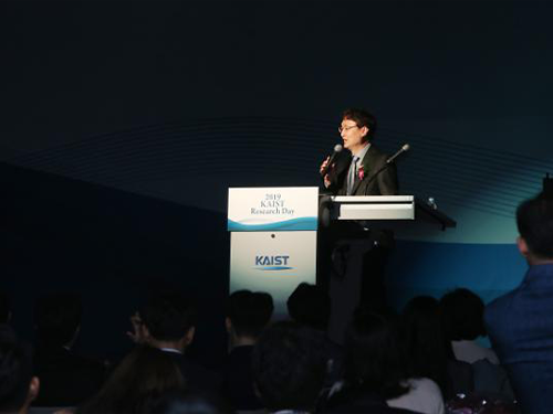
Professor Byung Jin Cho from the School of Electrical Engineering was selected as the Grand Research Prize Winner in recognition of his innovative research achievement in the fields of nano electric and flexible energy devices during the 2019 KAIST Research Day ceremony held on April 23 at the Chung Kunmo Conference Hall.
The ten most outstanding research achievements from the past year were also awarded in the three areas of Research, Innovation, Convergence Researches.
Professor Cho is an internationally recognized researcher in the field of future nano and energy device technology. Professor Cho’s team has continued to research on advanced CMOS (complementary metal-oxide semiconductors). CMOS has become his key research topic over the past three decades.
In 2014, he developed a glass fabric-based thermoelectric generator, which is extremely light and flexible and produces electricity from the heat of the human body. It is so flexible that the allowable bending radius of the generator is as low as 20 mm. There are no changes in performance even if the generator bends upward and downward for up to 120 cycles. His wearable thermoelectric generator was selected as one of the top ten most promising digital technologies by the Netexplo Forum in 2015.
He now is working on high-performance and ultra-flexible CMOS IC for biomedical applications, expanding his scope to thermal haptic technology in VR using graphene-CMOS hybrid integrated circuits; to self-powered wireless sensor nodes and self-powered ECG system using wearable thermoelectric generators .
In his special lecture at the ceremony, Professor Cho stressed the importance of collaboration in making scientific research and presented how he moved to future devices after focusing on scaling the devices.
“When I started the research on semiconductors, I focused on how to scale the device down as much as possible. For decades, we have conducted a number of procedures to produce tiny but efficient materials. Now we have shifted to develop flexible thermoelements and wearable devices,” said Professor Cho.
“We all thought the scaling down is the only way to create value-added technological breakthroughs. Now, the devices have been scaled down to 7nm and will go down to 5 nm soon. Over the past few years, I think we have gone through all the possible technological breakthroughs for reducing the size to 5nm. The semiconductor devices are made of more 1 billion transistors and go through 1,000 technological processes. So, there won’t be any possible way for a single genius to make a huge breakthrough. Without collaboration with others, it is nearly impossible to make any new technological breakthroughs.”
Professor Cho has published more than 240 papers in renowned academic journals and presented more than 300 papers at academic conferences. He has also registered approximately 50 patents in the field of semiconductor device technology.
The top ten research highlights of 2018 as follows:
- Rydberg-Atom Quantum Simulator Development by Professor Jaewook Ahn and Heung-Sun Sim from the Department of Physics
- From C-H to C-C Bonds at Room Temperature by Professor Mu-Hyun Baik from the Department of Chemistry
- The Role of Rodlike Counterions on the Interactions of DNAs by Professor Yong Woon Kim of the Graduate School of Nanoscience and Technology
- The Medal Preoptic Area Induces Hunting-Like Behaviors to Target Objects and Prey by Professor Daesoo Kim from the Department of Biological Sciences
- Identification of the Origin of Brain Tumors and New Therapeutic Strategy by Professor Jeong Ho Lee from the Graduate School of Medical Science and Engineering
- The Linear Frequency Conversion of Light at a Spatiotemporal Boundary by Professor Bumki Min from the Department of Mechanical Engineering
- An Industrial Grade Flexible Transparent Force Touch Sensor by Professor Jun-Bo Yoon from the School of Electrical Engineering
- The Detection and Clustering of Mixed-Type Defect Patterns in Wafer Bin Maps by Professor Heeyoung Kim from the Department of Industrial and Systems Engineering
- The Development of a Reconfigurable Spin-Based Logic Device by Professor Byong-Guk Park from the Department of Materials Science and Engineering
- The Development of a Miniaturized X-Ray Tube Based on Carbon Nanotube and Electronic Brachytherapy Device by Professor Sung Oh Cho from the Department of Nuclear and Quantum Engineering
Professor YongKeun Park from the Department of Physics and Professor In-Chel Park from the School of Electrical Engineering received the Research Award. For the Innovation Award, Professor Munchurl Kim from the School of Electrical Engineering was the recipient and the Convergence Research Awards was conferred to Professor Sung-Yool Choi from the School of Electrical Engineering, Professor Sung Gap Im from the Department of Chemical and Biomolecular Engineering, and Professor SangHee Park from the Department of Materials Science and Engineering during the ceremony.
For more on KAIST’s Top Research Achievements and Highlight of 2018, please refer to the attached below. click.
2019.04.25 View 26616
-
 Distinguished Professor Sang Yup Lee Participates in the 2014 Summer Davos Forum
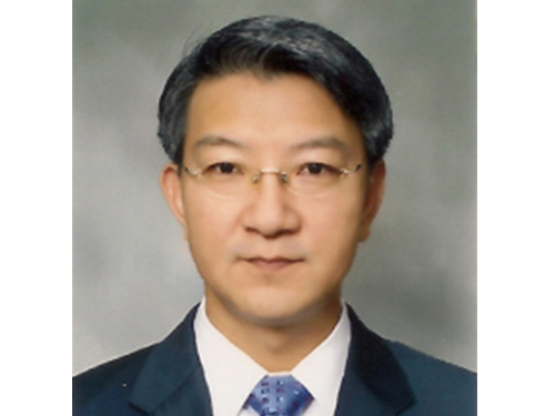
Distinguished Professor Sang Yup Lee from the Department of Chemical and Biomolecular Engineering, KAIST, was invited to lead four sessions at the Annual Meeting 2014, the World Economic Forum, also known as the Summer Davos Forum, which was held in Tianjin, China, from September 10th to 12th.
Two of the four sessions Professor Lee participated in were held on September 10th. At the first session entitled “Biotechnology Ecosystem,” he examined with other panelists the future of bioengineering in depth and discussed major policies and industry trends that will be necessary for the development of future biotechnologies.
Professor Lee later attended the “Strategic Shifts in Healthcare” session as a moderator. Issues related to transforming the health industry such as the next-generation genomics, mobile health and telemedicine, and wearable devices and predictive analytics were addressed.
On September 12, Professor Lee joined the “IdeasLab with KAIST” and gave a presentation on nanotechnology. There was a total of ten IdeasLab sessions held at the Summer Davos Forum, and KAIST was the only Korean university ever invited to host this session. In addition to Professor Lee’s presentation, three more presentations were made by KAIST professors on such topics as “Sustainable Energy and Materials” and “Next-generation Semiconductors.”
Lastly, Professor Lee participated in the “Global Promising Technology” session with the World Economic Forum’s Global Agenda Council members. At this session, he explained the selection of the “World’s Top 10 Most Promising Technologies” and “Bio Sector’s Top 10 Technologies” and led discussions about the “2015 Top 10 Technologies” with the council members.
The Davos Forum has been announcing the “World’s Top 10 Most Promising Technologies” since 2012, and Professor Lee has played a key role in the selection while working as the Chairman of Global Agenda Council. The selection results are presented at the Davos Forum every year and have attracted a lot of attention from around the world.
2014.09.15 View 20047