materials+science
-
 KAIST Research team develops anti-icing film that only requires sunlight
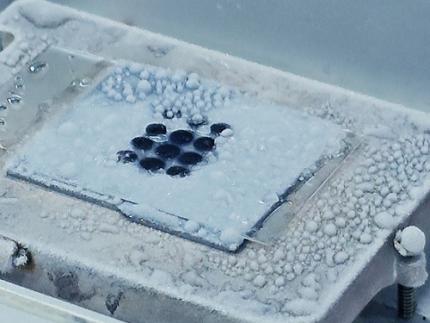
A KAIST research team has developed an anti-icing and de-icing film coating technology that can apply the photothermal effect of gold nanoparticles to industrial sites without the need for heating wires, periodic spray or oil coating of anti-freeze substances, and substrate design alterations.
The group led by Professor Hyoungsoo Kim from the Department of Mechanical Engineering (Fluid & Interface Laboratory) and Professor Dong Ki Yoon from the Department of Chemistry (Soft Material Assembly Group) revealed on January 3 to have together developed an original technique that can uniformly pattern gold nanorod (GNR) particles in quadrants through simple evaporation, and have used this to develop an anti-icing and de-icing surface.
Many scientists in recent years have tried to control substrate surfaces through various coating techniques, and those involving the patterning of functional nanomaterials have gained special attention. In particular, GNR is considered a promising candidate nanomaterial for its biocompatibility, chemical stability, relatively simple synthesis, and its stable and unique property of surface plasmon resonance. To maximize the performance of GNR, it is important to achieve a high uniformity during film deposition, and a high level of rod alignment. However, achieving both criteria has thus far been a difficult challenge.
< Figure 1. Conceptual image to display Hydrodynamic mechanisms for the formation of a homogeneous quadrant cellulose nanocrystal(CNC) matrix. >
To solve this, the joint research team utilized cellulose nanocrystal (CNC), a next-generation functional nanomaterial that can easily be extracted from nature. By co-assembling GNR on CNC quadrant templates, the team could uniformly dry the film and successfully obtain a GNR film with a uniform alignment in a ring-shape. Compared to existing coffee-ring films, the highly uniform and aligned GNR film developed through this research showed enhanced plasmonic photothermal properties, and the team showed that it could carry out anti-icing and de-icing functions by simply irradiating light in the visible wavelength range.
< Figure 2. Optical and thermal performance evaluation results of gold nanorod film and demonstration of plasmonic heater for anti-icing and de-icing. >
Professor Hyoungsoo Kim said, “This technique can be applied to plastic, as well as flexible surfaces. By using it on exterior materials and films, it can generate its own heat energy, which would greatly save energy through voluntary thermal energy harvesting across various applications including cars, aircrafts, and windows in residential or commercial spaces, where frosting becomes a serious issue in the winter.” Professor Dong Ki Yoon added, “This research is significant in that we can now freely pattern the CNC-GNR composite, which was previously difficult to create into films, over a large area. We can utilize this as an anti-icing material, and if we were to take advantage of the plasmonic properties of gold, we can also use it like stained-glass to decorate glass surfaces.”
This research was conducted by Ph.D. candidate Jeongsu Pyeon from the Department of Mechanical Engineering, and his co-first author Dr. Soon Mo Park (a KAIST graduate, currently a post-doctoral associate at Cornell University), and was pushed in the online volume of Nature Communication on December 8, 2023 under the title “Plasmonic Metasurfaces of Cellulose Nanocrystal Matrices with Quadrants of Aligned Gold Nanorods for Photothermal Anti-Icing." Recognized for its achievement, the research was also selected as an editor’s highlight for the journals Materials Science and Chemistry, and Inorganic and Physical Chemistry.
This research was supported by the Individual Basic Mid-Sized Research Fund from the National Research Foundation of Korea and the Center for Multiscale Chiral Architectures.
2024.01.16 View 4673
KAIST Research team develops anti-icing film that only requires sunlight
A KAIST research team has developed an anti-icing and de-icing film coating technology that can apply the photothermal effect of gold nanoparticles to industrial sites without the need for heating wires, periodic spray or oil coating of anti-freeze substances, and substrate design alterations.
The group led by Professor Hyoungsoo Kim from the Department of Mechanical Engineering (Fluid & Interface Laboratory) and Professor Dong Ki Yoon from the Department of Chemistry (Soft Material Assembly Group) revealed on January 3 to have together developed an original technique that can uniformly pattern gold nanorod (GNR) particles in quadrants through simple evaporation, and have used this to develop an anti-icing and de-icing surface.
Many scientists in recent years have tried to control substrate surfaces through various coating techniques, and those involving the patterning of functional nanomaterials have gained special attention. In particular, GNR is considered a promising candidate nanomaterial for its biocompatibility, chemical stability, relatively simple synthesis, and its stable and unique property of surface plasmon resonance. To maximize the performance of GNR, it is important to achieve a high uniformity during film deposition, and a high level of rod alignment. However, achieving both criteria has thus far been a difficult challenge.
< Figure 1. Conceptual image to display Hydrodynamic mechanisms for the formation of a homogeneous quadrant cellulose nanocrystal(CNC) matrix. >
To solve this, the joint research team utilized cellulose nanocrystal (CNC), a next-generation functional nanomaterial that can easily be extracted from nature. By co-assembling GNR on CNC quadrant templates, the team could uniformly dry the film and successfully obtain a GNR film with a uniform alignment in a ring-shape. Compared to existing coffee-ring films, the highly uniform and aligned GNR film developed through this research showed enhanced plasmonic photothermal properties, and the team showed that it could carry out anti-icing and de-icing functions by simply irradiating light in the visible wavelength range.
< Figure 2. Optical and thermal performance evaluation results of gold nanorod film and demonstration of plasmonic heater for anti-icing and de-icing. >
Professor Hyoungsoo Kim said, “This technique can be applied to plastic, as well as flexible surfaces. By using it on exterior materials and films, it can generate its own heat energy, which would greatly save energy through voluntary thermal energy harvesting across various applications including cars, aircrafts, and windows in residential or commercial spaces, where frosting becomes a serious issue in the winter.” Professor Dong Ki Yoon added, “This research is significant in that we can now freely pattern the CNC-GNR composite, which was previously difficult to create into films, over a large area. We can utilize this as an anti-icing material, and if we were to take advantage of the plasmonic properties of gold, we can also use it like stained-glass to decorate glass surfaces.”
This research was conducted by Ph.D. candidate Jeongsu Pyeon from the Department of Mechanical Engineering, and his co-first author Dr. Soon Mo Park (a KAIST graduate, currently a post-doctoral associate at Cornell University), and was pushed in the online volume of Nature Communication on December 8, 2023 under the title “Plasmonic Metasurfaces of Cellulose Nanocrystal Matrices with Quadrants of Aligned Gold Nanorods for Photothermal Anti-Icing." Recognized for its achievement, the research was also selected as an editor’s highlight for the journals Materials Science and Chemistry, and Inorganic and Physical Chemistry.
This research was supported by the Individual Basic Mid-Sized Research Fund from the National Research Foundation of Korea and the Center for Multiscale Chiral Architectures.
2024.01.16 View 4673 -
 Big Ideas on Emerging Materials Explored at EMS
Renowned scholars and editors from academic journals joined the Emerging Materials e-Symposium (EMS) held at KAIST and shared the latest breakthroughs and big ideas in new material development last month. This e-symposium was organized by Professor Il-Doo Kim from the KAIST Department of Materials Sciences and Engineering over five days from September 21 through 25 via Zoom and YouTube. Professor Kim also serves as an associate editor of ACS Nano.
Esteemed scholars and editors of academic journals including ACS Nano, Nano Energy, and Energy Storage Materials made Zoom presentations in three main categories: 1) nanostructures for next-generation applications, 2) chemistry and biotechnology for applications in the fields of environment and industry, and 3) material innovation for technological applications.
During Session I, speakers including Professor John A. Rogers of Northwestern University and Professor Zhenan Bao of Stanford University led the session on Emerging Soft Electronics and 3D printing.
In later sessions, other globally recognized scholars gave talks titled Advanced Nanostructuring for Emerging Materials, Frontiers in Emerging Materials Research, Advanced Energy Materials and Functional Nanomaterials, and Latest Advances in Nanomaterials Research.
These included 2010 Nobel Prize laureate and professor at Manchester University Andre Geim, editor-in-chief of ACS Nano and professor at UCLA Paul S. Weiss, Professor Paul Alivisatos of UC Berkeley, Professor William Chueh of Stanford University, and Professor Mircea Dinca of MIT.
KAIST President Sung-Chul Shin, who is also a materials physicist, said in his opening address, “Innovation in materials science will become an important driving force to change our way of life. All the breakthroughs in materials have extended a new paradigm that has transformed our lives.”
“Creative research projects alongside global collaborators like all of you will allow the breakthroughs that will deliver us from these crises,” he added.
(END)
2020.10.06 View 10516
Big Ideas on Emerging Materials Explored at EMS
Renowned scholars and editors from academic journals joined the Emerging Materials e-Symposium (EMS) held at KAIST and shared the latest breakthroughs and big ideas in new material development last month. This e-symposium was organized by Professor Il-Doo Kim from the KAIST Department of Materials Sciences and Engineering over five days from September 21 through 25 via Zoom and YouTube. Professor Kim also serves as an associate editor of ACS Nano.
Esteemed scholars and editors of academic journals including ACS Nano, Nano Energy, and Energy Storage Materials made Zoom presentations in three main categories: 1) nanostructures for next-generation applications, 2) chemistry and biotechnology for applications in the fields of environment and industry, and 3) material innovation for technological applications.
During Session I, speakers including Professor John A. Rogers of Northwestern University and Professor Zhenan Bao of Stanford University led the session on Emerging Soft Electronics and 3D printing.
In later sessions, other globally recognized scholars gave talks titled Advanced Nanostructuring for Emerging Materials, Frontiers in Emerging Materials Research, Advanced Energy Materials and Functional Nanomaterials, and Latest Advances in Nanomaterials Research.
These included 2010 Nobel Prize laureate and professor at Manchester University Andre Geim, editor-in-chief of ACS Nano and professor at UCLA Paul S. Weiss, Professor Paul Alivisatos of UC Berkeley, Professor William Chueh of Stanford University, and Professor Mircea Dinca of MIT.
KAIST President Sung-Chul Shin, who is also a materials physicist, said in his opening address, “Innovation in materials science will become an important driving force to change our way of life. All the breakthroughs in materials have extended a new paradigm that has transformed our lives.”
“Creative research projects alongside global collaborators like all of you will allow the breakthroughs that will deliver us from these crises,” he added.
(END)
2020.10.06 View 10516 -
 KAIST Professors Selected as Y-KAST Members
Professor YongKeun Park, Professor Bumjoon Kim, Professor Keon Jae Lee, and Professor Young Seok Ju were selected as the newest members of the Young Korean Academy of Science and Technology (Y-KAST).
The Korean Academy of Science and Technology, an academic institution of professional experts, selected 26 promising scientists under the age of 43 to join Y-KAST. and four KAIST professors were included in the list.
The newest members were conferred on February 26.
Research Field
Name
Natural Sciences
YongKeun Park (Dept. of Physics)
Engineering
Bumjoon Kim (Dept. of Chemical and Biomolecular Engineering)
Agricultural & Fishery Sciences
Keon Jae Lee (Dept. of Materials Science and Engineering)
Medical Sciences
Young Seok Ju (Graduate School of Medical Science and Engineering)
2018.03.05 View 6931
KAIST Professors Selected as Y-KAST Members
Professor YongKeun Park, Professor Bumjoon Kim, Professor Keon Jae Lee, and Professor Young Seok Ju were selected as the newest members of the Young Korean Academy of Science and Technology (Y-KAST).
The Korean Academy of Science and Technology, an academic institution of professional experts, selected 26 promising scientists under the age of 43 to join Y-KAST. and four KAIST professors were included in the list.
The newest members were conferred on February 26.
Research Field
Name
Natural Sciences
YongKeun Park (Dept. of Physics)
Engineering
Bumjoon Kim (Dept. of Chemical and Biomolecular Engineering)
Agricultural & Fishery Sciences
Keon Jae Lee (Dept. of Materials Science and Engineering)
Medical Sciences
Young Seok Ju (Graduate School of Medical Science and Engineering)
2018.03.05 View 6931 -
 Professor Il-Doo Kim Recevies the Song-gok Award
Professor Il-Doo Kim from the Department of Materials Science and Engineering at KAIST received the 20th Song-gok Science and Technology Award from Korea Institute of Science and Technology (KSIT).
The Song-gok Science and Technology Award was established to praise the accomplishments of the first president, Hyung-seop Choi, whose penname is Song-gok. The award selects a recipient in the field of materials and technology every other year.
Professor Kim, in recognition of his outstanding research and contributions to materials science in Korea, received the award during the 52nd anniversary ceremony of KIST on February 9.
Professor Kim focuses on developing nanofiber gas sensors for diagnosing disease in advance by analyzing exhaled biomarkers with electrospinning technology.
He has published more than 211 papers and has recorded more than 9,650 citations and 50 h-index.
Professor Kim has registered 107 patents and applied 38 patents in Korea while registering 29 patents and applying 16 patents overseas. Also, he transferred four technologies in 2017.
Professor Kim is recognized as one of the researchers who is leading nanofiber technology. On January 17, he made a keynote speech at the 5th International Conference on Electrospinning, which was his fourth keynote speech at that conference.
Moreover, he received the Technology Innovation Award at the College of Engineering, KAIST on December 19, 2017.
Professor Kim said, “It is my great honor to receive the Song-gok Science and Technology Award. I would like to bring distinction to KAIST by taking the lead in the commercializing a nanofiber-based highly sensitive nanosensors, diversifying and commercializing technology using nanofiber.”
2018.02.13 View 6282
Professor Il-Doo Kim Recevies the Song-gok Award
Professor Il-Doo Kim from the Department of Materials Science and Engineering at KAIST received the 20th Song-gok Science and Technology Award from Korea Institute of Science and Technology (KSIT).
The Song-gok Science and Technology Award was established to praise the accomplishments of the first president, Hyung-seop Choi, whose penname is Song-gok. The award selects a recipient in the field of materials and technology every other year.
Professor Kim, in recognition of his outstanding research and contributions to materials science in Korea, received the award during the 52nd anniversary ceremony of KIST on February 9.
Professor Kim focuses on developing nanofiber gas sensors for diagnosing disease in advance by analyzing exhaled biomarkers with electrospinning technology.
He has published more than 211 papers and has recorded more than 9,650 citations and 50 h-index.
Professor Kim has registered 107 patents and applied 38 patents in Korea while registering 29 patents and applying 16 patents overseas. Also, he transferred four technologies in 2017.
Professor Kim is recognized as one of the researchers who is leading nanofiber technology. On January 17, he made a keynote speech at the 5th International Conference on Electrospinning, which was his fourth keynote speech at that conference.
Moreover, he received the Technology Innovation Award at the College of Engineering, KAIST on December 19, 2017.
Professor Kim said, “It is my great honor to receive the Song-gok Science and Technology Award. I would like to bring distinction to KAIST by taking the lead in the commercializing a nanofiber-based highly sensitive nanosensors, diversifying and commercializing technology using nanofiber.”
2018.02.13 View 6282 -
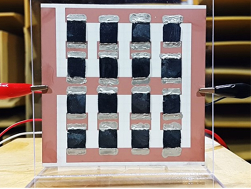 Extremely Thin and Highly Flexible Graphene-Based Thermoacoustic Speakers
A joint research team led by Professors Jung-Woo Choi and Byung Jin Cho of the School of Electrical Engineering and Professor Sang Ouk Kim of the Material Science and Engineering Department, all on the faculty of the Korea Advanced Institute of Science and Technology (KAIST), has developed a simpler way to mass-produce ultra-thin graphene thermosacoustic speakers.
Their research results were published online on August 17, 2016 in a journal called Applied Materials & Interfaces. The IEEE Spectrum, a monthly magazine published by the Institute of Electrical and Electronics Engineers, reported on the research on September 9, 2016, in an article titled, “Graphene Enables Flat Speakers for Mobile Audio Systems.” The American Chemical Society also drew attention to the team’s work in its article dated September 7, 2016, “Bringing Graphene Speakers to the Mobile Market.”
Thermoacoustic speakers generate sound waves from temperature fluctuations by rapidly heating and cooling conducting materials. Unlike conventional voice-coil speakers, thermoacoustic speakers do not rely on vibrations to produce sound, and thus do not need bulky acoustic boxes to keep complicated mechanical parts for sound production. They also generate good quality sound in all directions, enabling them to be placed on any surface including curved ones without canceling out sounds generated from opposite sides.
Based on a two-step, template-free fabrication method that involved freeze-drying a solution of graphene oxide flakes and the reduction/doping of oxidized graphene to improve electrical properties, the research team produced a N-doped, three-dimensional (3D), reduced graphene oxide aerogel (N-rGOA) with a porous macroscopic structure that permitted easy modulation for many potential applications.
Using 3D graphene aerogels, the team succeeded in fabricating an array of loudspeakers that were able to withstand over 40 W input power and that showed excellent sound pressure level (SPL), comparable to those of previously reported 2D and 3D graphene loudspeakers.
Choong Sun Kim, the lead author of the research paper and a doctoral student in the School of Electrical Engineering at KAIST, said:
“Thermoacoustic speakers have a higher efficiency when conducting materials have a smaller heat capacity. Nanomaterials such as graphene are an ideal candidate for conductors, but they require a substrate to support their extremely thinness. The substrate’s tendency to lose heat lowers the speakers’ efficiency. Here, we developed 3D graphene aerogels without a substrate by using a simple two-step process. With graphene aerogels, we have fabricated an array of loudspeakers that demonstrated stable performance. This is a practical technology that will enable mass-production of thermosacoustic speakers including on mobile platforms.”
The research paper is entitled “Application of N-Doped Three-Dimensional Reduced Graphene Oxide Aerogel to Thin Film Loudspeaker.” (DOI: 10.1021/acsami.6b03618)
Figure 1: A Thermoacoustic Loudspeaker Consisted of an Array of 16 3D Graphene Aerogels
Figure 2: Two-step Fabrication Process of 3D Reduced Graphene Oxide Aerogel Using Freeze-Drying and Reduction/Doping
Figure 3: X-ray Photoelectron Spectroscopy Graph of the 3D Reduced Graphene Oxide Aerogel and Its Scanning Electron Microscope Image
2016.10.05 View 10637
Extremely Thin and Highly Flexible Graphene-Based Thermoacoustic Speakers
A joint research team led by Professors Jung-Woo Choi and Byung Jin Cho of the School of Electrical Engineering and Professor Sang Ouk Kim of the Material Science and Engineering Department, all on the faculty of the Korea Advanced Institute of Science and Technology (KAIST), has developed a simpler way to mass-produce ultra-thin graphene thermosacoustic speakers.
Their research results were published online on August 17, 2016 in a journal called Applied Materials & Interfaces. The IEEE Spectrum, a monthly magazine published by the Institute of Electrical and Electronics Engineers, reported on the research on September 9, 2016, in an article titled, “Graphene Enables Flat Speakers for Mobile Audio Systems.” The American Chemical Society also drew attention to the team’s work in its article dated September 7, 2016, “Bringing Graphene Speakers to the Mobile Market.”
Thermoacoustic speakers generate sound waves from temperature fluctuations by rapidly heating and cooling conducting materials. Unlike conventional voice-coil speakers, thermoacoustic speakers do not rely on vibrations to produce sound, and thus do not need bulky acoustic boxes to keep complicated mechanical parts for sound production. They also generate good quality sound in all directions, enabling them to be placed on any surface including curved ones without canceling out sounds generated from opposite sides.
Based on a two-step, template-free fabrication method that involved freeze-drying a solution of graphene oxide flakes and the reduction/doping of oxidized graphene to improve electrical properties, the research team produced a N-doped, three-dimensional (3D), reduced graphene oxide aerogel (N-rGOA) with a porous macroscopic structure that permitted easy modulation for many potential applications.
Using 3D graphene aerogels, the team succeeded in fabricating an array of loudspeakers that were able to withstand over 40 W input power and that showed excellent sound pressure level (SPL), comparable to those of previously reported 2D and 3D graphene loudspeakers.
Choong Sun Kim, the lead author of the research paper and a doctoral student in the School of Electrical Engineering at KAIST, said:
“Thermoacoustic speakers have a higher efficiency when conducting materials have a smaller heat capacity. Nanomaterials such as graphene are an ideal candidate for conductors, but they require a substrate to support their extremely thinness. The substrate’s tendency to lose heat lowers the speakers’ efficiency. Here, we developed 3D graphene aerogels without a substrate by using a simple two-step process. With graphene aerogels, we have fabricated an array of loudspeakers that demonstrated stable performance. This is a practical technology that will enable mass-production of thermosacoustic speakers including on mobile platforms.”
The research paper is entitled “Application of N-Doped Three-Dimensional Reduced Graphene Oxide Aerogel to Thin Film Loudspeaker.” (DOI: 10.1021/acsami.6b03618)
Figure 1: A Thermoacoustic Loudspeaker Consisted of an Array of 16 3D Graphene Aerogels
Figure 2: Two-step Fabrication Process of 3D Reduced Graphene Oxide Aerogel Using Freeze-Drying and Reduction/Doping
Figure 3: X-ray Photoelectron Spectroscopy Graph of the 3D Reduced Graphene Oxide Aerogel and Its Scanning Electron Microscope Image
2016.10.05 View 10637 -
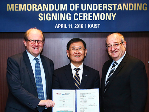 KAIST, NTU, and Technion Collaborate for Research in Emerging Fields
KAIST, Nanyang Technological University (NTU) of Singapore, and Technion of Israel signed an agreement on April 11, 2016 in Seoul to create a five-year joint research program for some of the most innovative and entrepreneurial areas: robotics, medical technologies, satellites, materials science and engineering, and entrepreneurship. Under the agreement, the universities will also offer dual degree opportunities, exchange visits, and internships.
In the picture from the left, Bertil Andersson of NTU, Sung-Mo Kang of KAIST, and Peretz Lavie of Technion hold the signed memorandum of understanding.
2016.04.14 View 8528
KAIST, NTU, and Technion Collaborate for Research in Emerging Fields
KAIST, Nanyang Technological University (NTU) of Singapore, and Technion of Israel signed an agreement on April 11, 2016 in Seoul to create a five-year joint research program for some of the most innovative and entrepreneurial areas: robotics, medical technologies, satellites, materials science and engineering, and entrepreneurship. Under the agreement, the universities will also offer dual degree opportunities, exchange visits, and internships.
In the picture from the left, Bertil Andersson of NTU, Sung-Mo Kang of KAIST, and Peretz Lavie of Technion hold the signed memorandum of understanding.
2016.04.14 View 8528 -
 President Steve Kang of KAIST Attends the 2014 Summer Davos Forum in Tianjin, China
President Steve Kang of KAIST will attend the 2014 Annual Meeting of the New Champions, the World Economic Forum (WEF), to be held on September 10-12, 2014 in Tianjin, China.
KAIST holds its own IdeasLab session on nanotechnology on September 12, 2014.
On September 10, 2014, President Steve Kang will participate in a private session hosted by the Global University Leaders Forum (GULF) community at WEF as a panelist.
In addition to President Kang, eight presidents from top global universities such as the National University of Singapore, Peking University, ETH Zurich (Swiss Federal Institute of Technology), University of Tokyo, and Carnegie Mellon University will join the panel discussion under the topic, “Increasing the Translational Impact of University Research.” Specifically, the presidents will address issues related to the importance of university-led technology transfer in Asia, key strategies and goals for technology transfer, and implementation approaches taken by each university to promote technology transfer from university to industry.
President Kang was invited to this GULF session, the only attendant from Korean universities, in recognition of his long time experience and expertise in education and research.
In 2006, WEF created the GULF, a small community of the presidents of top universities in the world, aiming to offer an open platform for high-level dialogues on issues of higher education and research with other sectors, as well as to foster collaboration between universities in areas of significance for global policy.
As of 2014, a total of 25 globally leading universities, including Harvard University, University of Cambridge, and Massachusetts Institute of Technology, are GULF members. KAIST, which joined the club this year, is the only Korean university.
The 2014 Annual Meeting of the New Champions, also known as the Summer Davos Forum, hosts numerous sessions under the theme of “Creating Value through Innovation.” At the Forum, a total of ten IdeasLab sessions will be hosted. KAIST was invited to run its own IdeasLab on nanotechnology on September 12, 2014.
Together with President Kang, Professors Sang Ouk Kim and Keon Jae Lee from the Department of Materials Science Engineering, KAIST, and Professors Sang Yup Lee and Hyunjoo Lee from the Department of Chemical and Biomolecular Engineering, KAIST, will present their own speeches on the topic entitled “From diagnostics to materials, how is nanotechnology changing lives?”
President Kang will give the opening speech at the KAIST IdeasLab.
He said that an invitation from WEF to join the IdeasLab spoke well for KAIST:
“KAIST is the first and the only Korean university ever invited to run its own IdeasLab at the World Economic Forum. The IdeasLab is an expert group meeting, conducted only by the world’s most prestigious universities and research institutes. At the IdeasLab sessions, global leaders from different sectors identify major issues facing higher education and humanity and explore solutions through science and technology innovation. Holding our own IdeasLab on one of our strongest fields, nanotechnology, is indeed an excellent opportunity for KAIST to show its strength in academic and research excellence on the global stage.”
2014.09.08 View 11365
President Steve Kang of KAIST Attends the 2014 Summer Davos Forum in Tianjin, China
President Steve Kang of KAIST will attend the 2014 Annual Meeting of the New Champions, the World Economic Forum (WEF), to be held on September 10-12, 2014 in Tianjin, China.
KAIST holds its own IdeasLab session on nanotechnology on September 12, 2014.
On September 10, 2014, President Steve Kang will participate in a private session hosted by the Global University Leaders Forum (GULF) community at WEF as a panelist.
In addition to President Kang, eight presidents from top global universities such as the National University of Singapore, Peking University, ETH Zurich (Swiss Federal Institute of Technology), University of Tokyo, and Carnegie Mellon University will join the panel discussion under the topic, “Increasing the Translational Impact of University Research.” Specifically, the presidents will address issues related to the importance of university-led technology transfer in Asia, key strategies and goals for technology transfer, and implementation approaches taken by each university to promote technology transfer from university to industry.
President Kang was invited to this GULF session, the only attendant from Korean universities, in recognition of his long time experience and expertise in education and research.
In 2006, WEF created the GULF, a small community of the presidents of top universities in the world, aiming to offer an open platform for high-level dialogues on issues of higher education and research with other sectors, as well as to foster collaboration between universities in areas of significance for global policy.
As of 2014, a total of 25 globally leading universities, including Harvard University, University of Cambridge, and Massachusetts Institute of Technology, are GULF members. KAIST, which joined the club this year, is the only Korean university.
The 2014 Annual Meeting of the New Champions, also known as the Summer Davos Forum, hosts numerous sessions under the theme of “Creating Value through Innovation.” At the Forum, a total of ten IdeasLab sessions will be hosted. KAIST was invited to run its own IdeasLab on nanotechnology on September 12, 2014.
Together with President Kang, Professors Sang Ouk Kim and Keon Jae Lee from the Department of Materials Science Engineering, KAIST, and Professors Sang Yup Lee and Hyunjoo Lee from the Department of Chemical and Biomolecular Engineering, KAIST, will present their own speeches on the topic entitled “From diagnostics to materials, how is nanotechnology changing lives?”
President Kang will give the opening speech at the KAIST IdeasLab.
He said that an invitation from WEF to join the IdeasLab spoke well for KAIST:
“KAIST is the first and the only Korean university ever invited to run its own IdeasLab at the World Economic Forum. The IdeasLab is an expert group meeting, conducted only by the world’s most prestigious universities and research institutes. At the IdeasLab sessions, global leaders from different sectors identify major issues facing higher education and humanity and explore solutions through science and technology innovation. Holding our own IdeasLab on one of our strongest fields, nanotechnology, is indeed an excellent opportunity for KAIST to show its strength in academic and research excellence on the global stage.”
2014.09.08 View 11365 -
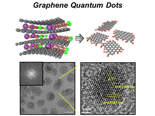 News Article on the Development of Synthesis Process for Graphene Quantum Dots
Before It's News, an international online news agency, highlighted the recent research conducted by KAIST professors (Seokwoo Jeon of the Department of Materials Science and Engineering, Yong-Hoon Cho of the Department of Physics, and Seunghyup Yoo of the Department of Electrical Engineering) on the development of synthesis process for graphene quantum dots, nanometer-sized round semiconductor nanoparticles that are very efficient at emitting photons. If commercialized, this synthetic technology will lead the way to the development of paper-thin displays in the future.
For the article, please go to the link below:
Before It’s News, September 3, 2014“Graphene quantum dots prove highly efficient in emitting light”
http://beforeitsnews.com/science-and-technology/2014/09/graphene-quantum-dots-prove-highly-efficient-in-emitting-light-2718190.html
2014.09.07 View 10786
News Article on the Development of Synthesis Process for Graphene Quantum Dots
Before It's News, an international online news agency, highlighted the recent research conducted by KAIST professors (Seokwoo Jeon of the Department of Materials Science and Engineering, Yong-Hoon Cho of the Department of Physics, and Seunghyup Yoo of the Department of Electrical Engineering) on the development of synthesis process for graphene quantum dots, nanometer-sized round semiconductor nanoparticles that are very efficient at emitting photons. If commercialized, this synthetic technology will lead the way to the development of paper-thin displays in the future.
For the article, please go to the link below:
Before It’s News, September 3, 2014“Graphene quantum dots prove highly efficient in emitting light”
http://beforeitsnews.com/science-and-technology/2014/09/graphene-quantum-dots-prove-highly-efficient-in-emitting-light-2718190.html
2014.09.07 View 10786 -
 A KAIST startup, YBrain, builds a wearable device to cure Alzheimer's
A group of KAIST graduates from the Departments of Bio and Brain Engineering, Computer Science, Materials Science Engineering, and Industrial Design created a startup called YBrain (http://ybrain.com/). YBrain develops a wearable neuroscience technology to treat or reduce the symptoms of degenerative brain diseases such as dementia and Alzheimer’s. Their recent technological developments were covered in e27, one of the leading blogs based in Singapore. The blog covers topics like the latest technology innovation, startups, and entrepreneurship in Asia. A news article follows below:
e27, June 24, 2014
“This wearable tech may be able to combat effects of Alzheimer’s”
http://e27.co/this-wearable-tech-may-be-able-combat-effects-of-alzheimers-20140624/
2014.06.25 View 9859
A KAIST startup, YBrain, builds a wearable device to cure Alzheimer's
A group of KAIST graduates from the Departments of Bio and Brain Engineering, Computer Science, Materials Science Engineering, and Industrial Design created a startup called YBrain (http://ybrain.com/). YBrain develops a wearable neuroscience technology to treat or reduce the symptoms of degenerative brain diseases such as dementia and Alzheimer’s. Their recent technological developments were covered in e27, one of the leading blogs based in Singapore. The blog covers topics like the latest technology innovation, startups, and entrepreneurship in Asia. A news article follows below:
e27, June 24, 2014
“This wearable tech may be able to combat effects of Alzheimer’s”
http://e27.co/this-wearable-tech-may-be-able-combat-effects-of-alzheimers-20140624/
2014.06.25 View 9859 -
 Ultra-High Strength Metamaterial Developed Using Graphene
New metamaterial has been developed, exhibiting hundreds of times greater strength than pure metals.
Professor Seung Min, Han and Yoo Sung, Jeong (Graduate School of Energy, Environment, Water, and Sustainability (EEWS)) and Professor Seok Woo, Jeon (Department of Material Science and Engineering) have developed a composite nanomaterial. The nanomaterial consists of graphene inserted in copper and nickel and exhibits strengths 500 times and 180 times, respectively, greater than that of pure metals. The result of the research was published on the July 2nd online edition in Nature Communications journal.
Graphene displays strengths 200 times greater than that of steel, is stretchable, and is flexible. The U.S. Army Armaments Research, Development and Engineering Center developed a graphene-metal nanomaterial but failed to drastically improve the strength of the material.
To maximize the strength increased by the addition of graphene, the KAIST research team created a layered structure of metal and graphene. Using CVD (Chemical Vapor Deposition), the team grew a single layer of graphene on a metal deposited substrate and then deposited another metal layer. They repeated this process to produce a metal-graphene multilayer composite material, utilizing a single layer of graphene. Micro-compression tests within Transmission Electronic Microscope and Molecular Dynamics simulations effectively showed the strength enhancing effect and the dislocation movement in grain boundaries of graphene on an atomic level.
The mechanical characteristics of the graphene layer within the metal-graphene composite material successfully blocked the dislocations and cracks from external damage from traveling inwards. Therefore the composite material displayed strength beyond conventional metal-metal multilayer materials. The copper-graphene multilayer material with an interplanar distance of 70nm exhibited 500 times greater (1.5GPa) strength than pure copper. Nickel-graphene multilayer material with an interplanar distance of 100nm showed 180 times greater (4.0GPa) strength than pure nickel.
It was found that there is a clear relationship between the interplanar distance and the strength of the multilayer material. A smaller interplanar distance made the dislocation movement more difficult and therefore increased the strength of the material. Professor Han, who led the research, commented, “the result is astounding as 0.00004% in weight of graphene increased the strength of the materials by hundreds of times” and “improvements based on this success, especially mass production with roll-to-roll process or metal sintering process in the production of ultra-high strength, lightweight parts for automobile and spacecraft, may become possible.” In addition, Professor Han mentioned that “the new material can be applied to coating materials for nuclear reactor construction or other structural materials requiring high reliability.”
The research project received support from National Research Foundation, Global Frontier Program, KAIST EEWS-KINC Program and KISTI Supercomputer and was a collaborative effort with KISTI (Korea Institute of Science and Technology Information), KBSI (Korea Basic Science Institute), Stanford University, and Columbia University.
A schematic diagram shows the structure of metal-graphene multi-layers. The metal-graphene multi-layered composite materials, containing a single-layered graphene, block the dislocation movement of graphene layers, resulting in a greater strength in the materials.
2013.08.23 View 12883
Ultra-High Strength Metamaterial Developed Using Graphene
New metamaterial has been developed, exhibiting hundreds of times greater strength than pure metals.
Professor Seung Min, Han and Yoo Sung, Jeong (Graduate School of Energy, Environment, Water, and Sustainability (EEWS)) and Professor Seok Woo, Jeon (Department of Material Science and Engineering) have developed a composite nanomaterial. The nanomaterial consists of graphene inserted in copper and nickel and exhibits strengths 500 times and 180 times, respectively, greater than that of pure metals. The result of the research was published on the July 2nd online edition in Nature Communications journal.
Graphene displays strengths 200 times greater than that of steel, is stretchable, and is flexible. The U.S. Army Armaments Research, Development and Engineering Center developed a graphene-metal nanomaterial but failed to drastically improve the strength of the material.
To maximize the strength increased by the addition of graphene, the KAIST research team created a layered structure of metal and graphene. Using CVD (Chemical Vapor Deposition), the team grew a single layer of graphene on a metal deposited substrate and then deposited another metal layer. They repeated this process to produce a metal-graphene multilayer composite material, utilizing a single layer of graphene. Micro-compression tests within Transmission Electronic Microscope and Molecular Dynamics simulations effectively showed the strength enhancing effect and the dislocation movement in grain boundaries of graphene on an atomic level.
The mechanical characteristics of the graphene layer within the metal-graphene composite material successfully blocked the dislocations and cracks from external damage from traveling inwards. Therefore the composite material displayed strength beyond conventional metal-metal multilayer materials. The copper-graphene multilayer material with an interplanar distance of 70nm exhibited 500 times greater (1.5GPa) strength than pure copper. Nickel-graphene multilayer material with an interplanar distance of 100nm showed 180 times greater (4.0GPa) strength than pure nickel.
It was found that there is a clear relationship between the interplanar distance and the strength of the multilayer material. A smaller interplanar distance made the dislocation movement more difficult and therefore increased the strength of the material. Professor Han, who led the research, commented, “the result is astounding as 0.00004% in weight of graphene increased the strength of the materials by hundreds of times” and “improvements based on this success, especially mass production with roll-to-roll process or metal sintering process in the production of ultra-high strength, lightweight parts for automobile and spacecraft, may become possible.” In addition, Professor Han mentioned that “the new material can be applied to coating materials for nuclear reactor construction or other structural materials requiring high reliability.”
The research project received support from National Research Foundation, Global Frontier Program, KAIST EEWS-KINC Program and KISTI Supercomputer and was a collaborative effort with KISTI (Korea Institute of Science and Technology Information), KBSI (Korea Basic Science Institute), Stanford University, and Columbia University.
A schematic diagram shows the structure of metal-graphene multi-layers. The metal-graphene multi-layered composite materials, containing a single-layered graphene, block the dislocation movement of graphene layers, resulting in a greater strength in the materials.
2013.08.23 View 12883 -
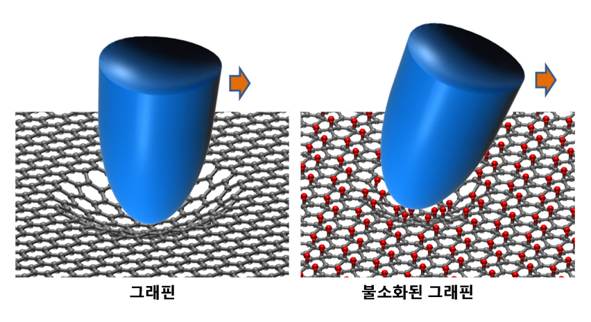 KAIST researchers verify and control the mechanical properties of graphene
KAIST researchers have successfully verified and controlled the mechanical properties of graphene, a next-generation material. Professor Park Jung Yong from the EEWS Graduate School and Professor Kim Yong Hyun from the Graduate School of Nanoscience and Technology have succeeded in fluorinating a single atomic-layered graphene sample and controlling its frictional and adhesive properties. This is the first time the frictional properties of graphene have been examined at the atomic level, and the technology is expected to be applied to nano-sized robots and microscopic joints.
Graphene is often dubbed “the dream material” because of its ability to conduct high amounts of electricity even when bent, making it the next-generation substitute for silicon semiconductors, paving the way for flexible display and wearable computer technologies. Graphene also has high potential applications in mechanical engineering because of its great material strength, but its mechanical properties remained elusive until now.
Professor Park’s research team successfully produced individual graphene samples with fluorine-deficiency at the atomic level by placing the samples in Fluoro-xenon (XeF2) gas and applying heat. The surface of the graphene was scanned using a micro probe and a high vacuum atomic microscope to measure its dynamic properties.
The research team found that the fluorinated graphene sample had 6 times more friction and 0.7 times more adhesiveness than the original graphene. Electrical measurements confirmed the fluorination process, and the analysis of the findings helped setup the theory of frictional changes in graphene.
Professor Park stated that “graphene can be used for the lubrication of joints in nano-sized devices” and that this research has numerous applications such as the coating of graphene-based microdynamic devices.
This research was published in the online June edition of Nano Letters and was supported by the Ministry of Science, Technology, and Education and the National Research Foundation as part of the World Class University (WCU) program.
2012.07.24 View 12796
KAIST researchers verify and control the mechanical properties of graphene
KAIST researchers have successfully verified and controlled the mechanical properties of graphene, a next-generation material. Professor Park Jung Yong from the EEWS Graduate School and Professor Kim Yong Hyun from the Graduate School of Nanoscience and Technology have succeeded in fluorinating a single atomic-layered graphene sample and controlling its frictional and adhesive properties. This is the first time the frictional properties of graphene have been examined at the atomic level, and the technology is expected to be applied to nano-sized robots and microscopic joints.
Graphene is often dubbed “the dream material” because of its ability to conduct high amounts of electricity even when bent, making it the next-generation substitute for silicon semiconductors, paving the way for flexible display and wearable computer technologies. Graphene also has high potential applications in mechanical engineering because of its great material strength, but its mechanical properties remained elusive until now.
Professor Park’s research team successfully produced individual graphene samples with fluorine-deficiency at the atomic level by placing the samples in Fluoro-xenon (XeF2) gas and applying heat. The surface of the graphene was scanned using a micro probe and a high vacuum atomic microscope to measure its dynamic properties.
The research team found that the fluorinated graphene sample had 6 times more friction and 0.7 times more adhesiveness than the original graphene. Electrical measurements confirmed the fluorination process, and the analysis of the findings helped setup the theory of frictional changes in graphene.
Professor Park stated that “graphene can be used for the lubrication of joints in nano-sized devices” and that this research has numerous applications such as the coating of graphene-based microdynamic devices.
This research was published in the online June edition of Nano Letters and was supported by the Ministry of Science, Technology, and Education and the National Research Foundation as part of the World Class University (WCU) program.
2012.07.24 View 12796 -
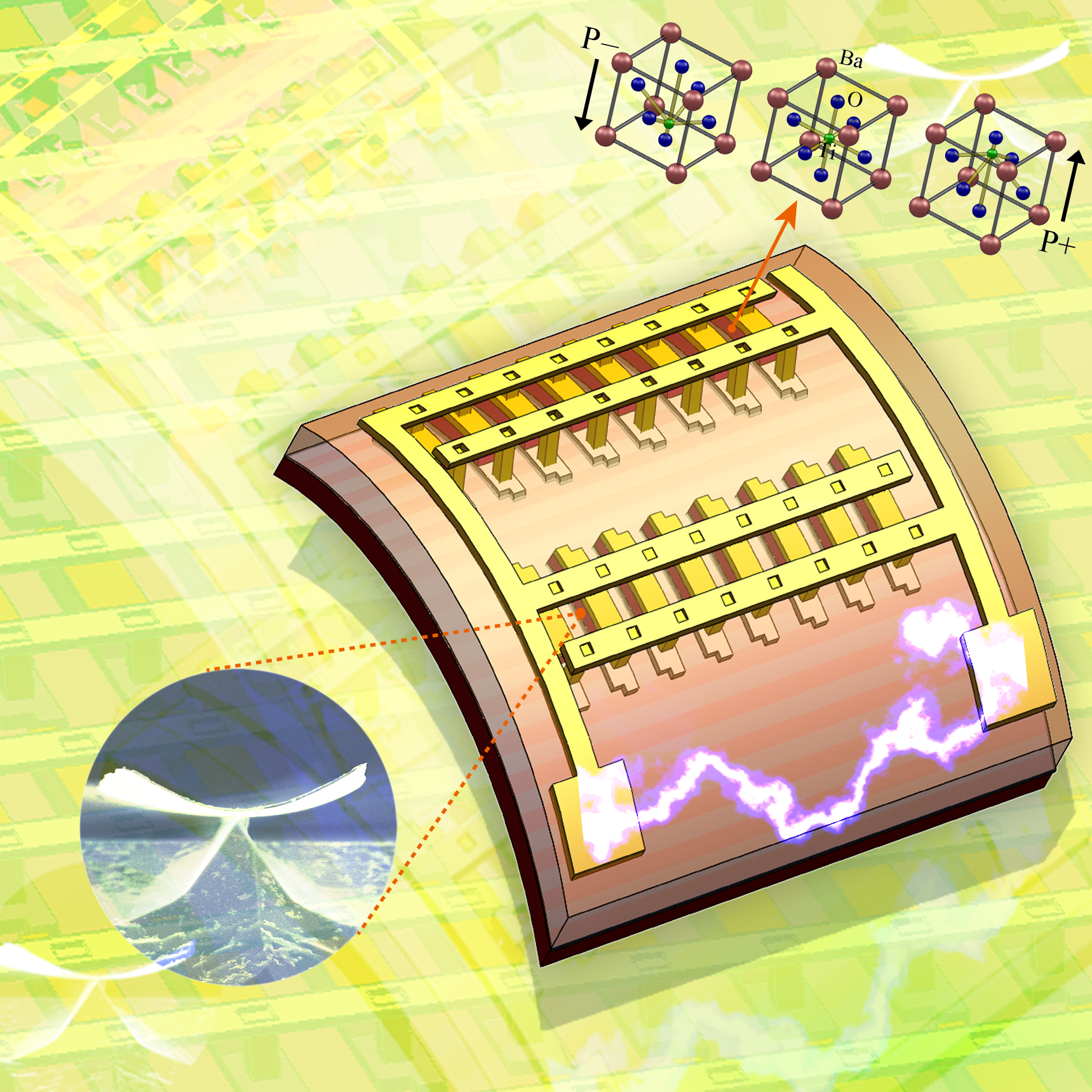 The KAIST & GIT team developed a power generation technology using bendable thin film nano-materials.
Figure description: Flexible thin film nanomaterials produce electricity.
Can a heart implanted micro robot operate permanently?
Can cell phones and tiny robots implanted in the heart operate permanently without having their batteries charged?
It might sound like science fiction, but these things seem to be possible in the near future. The team of Prof. Keon Jae Lee (KAIST, Dept. of Materials Science and Engineering) and Prof. Zhong Lin Wang (Georgia Institute of Technology, Dept. of Materials Science and Engineering) has developed new forms of highly efficient, flexible nanogenerator technology using the freely bendable piezoelectric ceramic thin film nano-materials that can convert tiny movements of the human body (such as heart beats and blood flow) into electrical energy.
The piezoelectric effect refers to voltage generation when pressure or bending strength is applied to piezoelectric materials. The ceramics, containing a perovskite structure, have a high piezoelectric efficiency. Until now, it has been very difficult to use these ceramic materials to fabricate flexible electronic systems due to their brittle property.
The research team, however, has succeeded in developing a bio-eco-friendly ceramic thin film nanogenerator that is freely bendable without breakdown.
Nanogenerator technology, a power generating system without wires or batteries, combines nanotechnology with piezoelectrics that can be used not only in personal mobile electronics but also in bio-implantable sensors or as an energy source for micro robots. Energy sources in nature (wind, vibration, and sound) and biomechanical forces produced by the human body (heart beats, blood flow, and muscle contraction/relaxation) can infinitely produce nonpolluting energy. (Nanogenerator produces electricity by external forces: http://www.youtube.com/watch?v=tvj0SsBqpBw)
Prof. Keon Jae Lee (KAIST) was involved in the first co-invention of “High Performance Flexible Single Crystal Electronics” during his PhD course at the University of Illinois at Urbana-Champaign. This nanogenerator technology, based on the previous invention, utilized the similar protocol of transferring ceramic thin film nano-materials on flexible substrates and produced voltage generation between electrodes.
Prof. Zhong Lin Wang (Georgia Tech, inventor of the nanogenerator) said, “This technology can be used to turn on an LED by slightly modifying circuits and operate touchable flexible displays. In addition, thin film nano-materials (‘barium titanate’) of this research have the property of both high efficiency and lead-free bio compatibility, which can be used in future medical applications.” This result is published in November online issue of ‘Nano Letters’ ACS journal.
<Video>
Youtube link: http://www.youtube.com/watch?v=tvj0SsBqpBw
Thin Film Nanogenerator produces electricity by external forces.
2010.11.23 View 12604
The KAIST & GIT team developed a power generation technology using bendable thin film nano-materials.
Figure description: Flexible thin film nanomaterials produce electricity.
Can a heart implanted micro robot operate permanently?
Can cell phones and tiny robots implanted in the heart operate permanently without having their batteries charged?
It might sound like science fiction, but these things seem to be possible in the near future. The team of Prof. Keon Jae Lee (KAIST, Dept. of Materials Science and Engineering) and Prof. Zhong Lin Wang (Georgia Institute of Technology, Dept. of Materials Science and Engineering) has developed new forms of highly efficient, flexible nanogenerator technology using the freely bendable piezoelectric ceramic thin film nano-materials that can convert tiny movements of the human body (such as heart beats and blood flow) into electrical energy.
The piezoelectric effect refers to voltage generation when pressure or bending strength is applied to piezoelectric materials. The ceramics, containing a perovskite structure, have a high piezoelectric efficiency. Until now, it has been very difficult to use these ceramic materials to fabricate flexible electronic systems due to their brittle property.
The research team, however, has succeeded in developing a bio-eco-friendly ceramic thin film nanogenerator that is freely bendable without breakdown.
Nanogenerator technology, a power generating system without wires or batteries, combines nanotechnology with piezoelectrics that can be used not only in personal mobile electronics but also in bio-implantable sensors or as an energy source for micro robots. Energy sources in nature (wind, vibration, and sound) and biomechanical forces produced by the human body (heart beats, blood flow, and muscle contraction/relaxation) can infinitely produce nonpolluting energy. (Nanogenerator produces electricity by external forces: http://www.youtube.com/watch?v=tvj0SsBqpBw)
Prof. Keon Jae Lee (KAIST) was involved in the first co-invention of “High Performance Flexible Single Crystal Electronics” during his PhD course at the University of Illinois at Urbana-Champaign. This nanogenerator technology, based on the previous invention, utilized the similar protocol of transferring ceramic thin film nano-materials on flexible substrates and produced voltage generation between electrodes.
Prof. Zhong Lin Wang (Georgia Tech, inventor of the nanogenerator) said, “This technology can be used to turn on an LED by slightly modifying circuits and operate touchable flexible displays. In addition, thin film nano-materials (‘barium titanate’) of this research have the property of both high efficiency and lead-free bio compatibility, which can be used in future medical applications.” This result is published in November online issue of ‘Nano Letters’ ACS journal.
<Video>
Youtube link: http://www.youtube.com/watch?v=tvj0SsBqpBw
Thin Film Nanogenerator produces electricity by external forces.
2010.11.23 View 12604