light
-
 KAIST's Li-Fi - Achieves 100 Times Faster Speed and Enhanced Security of Wi-Fi
- KAIST-KRISS Develop 'On-Device Encryption Optical Transmitter' Based on Eco-Friendly Quantum Dots
- New Li-Fi Platform Technology Achieves High Performance with 17.4% Device Efficiency and 29,000 nit Brightness, Simultaneously Improving Transmission Speed and Security
- Presents New Methodology for High-Speed and Encrypted Communication Through Single-Device-Based Dual-Channel Optical Modulation
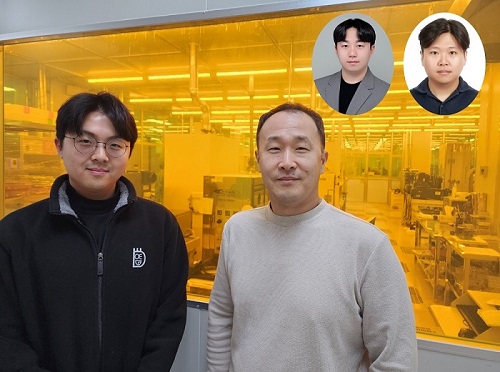
< Photo 1. (Front row from left) Seungmin Shin, First Author; Professor Himchan Cho; (Back row from left) Hyungdoh Lee, Seungwoo Lee, Wonbeom Lee; (Top left) Dr. Kyung-geun Lim >
Li-Fi (Light Fidelity) is a wireless communication technology that utilizes the visible light spectrum (400-800 THz), similar to LED light, offering speeds up to 100 times faster than existing Wi-Fi (up to 224 Gbps). While it has fewer limitations in available frequency allocation and less radio interference, it is relatively vulnerable to security breaches as anyone can access it. Korean researchers have now proposed a new Li-Fi platform that overcomes the limitations of conventional optical communication devices and can simultaneously enhance both transmission speed and security.
KAIST (President Kwang Hyung Lee) announced on the 24th that Professor Himchan Cho's research team from the Department of Materials Science and Engineering, in collaboration with Dr. Kyung-geun Lim of the Korea Research Institute of Standards and Science (KRISS, President Ho-Seong Lee) under the National Research Council of Science & Technology (NST, Chairman Young-Sik Kim), has developed 'on-device encryption optical communication device' technology for the utilization of 'Li-Fi,' which is attracting attention as a next-generation ultra-high-speed data communication.
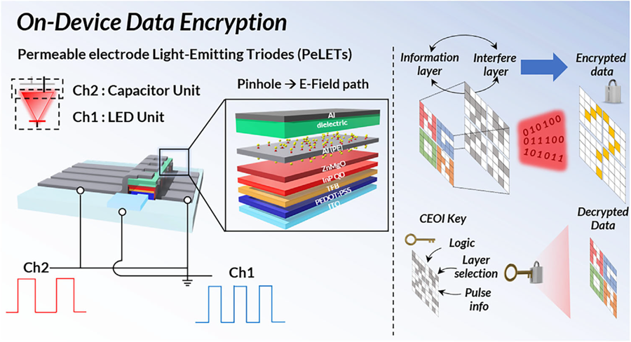
Professor Cho's team created high-efficiency light-emitting triode devices using eco-friendly quantum dots (low-toxicity and sustainable materials). The device developed by the research team is a mechanism that generates light using an electric field. Specifically, the electric field is concentrated in 'tiny holes (pinholes) in the permeable electrode' and transmitted beyond the electrode. This device utilizes this principle to simultaneously process two input data streams.
Using this principle, the research team developed a technology called 'on-device encryption optical transmitter.' The core of this technology is that the device itself converts information into light and simultaneously encrypts it. This means that enhanced security data transmission is possible without the need for complex, separate equipment.
External Quantum Efficiency (EQE) is an indicator of how efficiently electricity is converted into light, with a general commercialization standard of about 20%. The newly developed device recorded an EQE of 17.4%, and its luminance was 29,000 nit, significantly exceeding the maximum brightness of a smartphone OLED screen, which is 2,000 nit, demonstrating a brightness more than 10 times higher.
< Figure 1. Schematic diagram of the device structure developed by the research team and encrypted communication >
Furthermore, to more accurately understand how this device converts information into light, the research team used a method called 'transient electroluminescence analysis.' They analyzed the light-emitting characteristics generated by the device when voltage was instantaneously applied for very short durations (hundreds of nanoseconds = billionths of a second). Through this analysis, they investigated the movement of charges within the device at hundreds of nanoseconds, elucidating the operating mechanism of dual-channel optical modulation implemented within a single device.
Professor Himchan Cho of KAIST stated, "This research overcomes the limitations of existing optical communication devices and proposes a new communication platform that can both increase transmission speed and enhance security."
< Photo 2. Professor Himchan Cho, Department of Materials Science and Engineering >
He added, "This technology, which strengthens security without additional equipment and simultaneously enables encryption and transmission, can be widely applied in various fields where security is crucial in the future."
This research, with Seungmin Shin, a Ph.D. candidate at KAIST's Department of Materials Science and Engineering, participating as the first author, and Professor Himchan Cho and Dr. Kyung-geun Lim of KRISS as co-corresponding authors, was published in the international journal 'Advanced Materials' on May 30th and was selected as an inside front cover paper.※ Paper Title: High-Efficiency Quantum Dot Permeable electrode Light-Emitting Triodes for Visible-Light Communications and On-Device Data Encryption※ DOI: https://doi.org/10.1002/adma.202503189
This research was supported by the National Research Foundation of Korea, the National Research Council of Science & Technology (NST), and the Korea Institute for Advancement of Technology.
2025.06.24 View 1952
KAIST's Li-Fi - Achieves 100 Times Faster Speed and Enhanced Security of Wi-Fi
- KAIST-KRISS Develop 'On-Device Encryption Optical Transmitter' Based on Eco-Friendly Quantum Dots
- New Li-Fi Platform Technology Achieves High Performance with 17.4% Device Efficiency and 29,000 nit Brightness, Simultaneously Improving Transmission Speed and Security
- Presents New Methodology for High-Speed and Encrypted Communication Through Single-Device-Based Dual-Channel Optical Modulation
< Photo 1. (Front row from left) Seungmin Shin, First Author; Professor Himchan Cho; (Back row from left) Hyungdoh Lee, Seungwoo Lee, Wonbeom Lee; (Top left) Dr. Kyung-geun Lim >
Li-Fi (Light Fidelity) is a wireless communication technology that utilizes the visible light spectrum (400-800 THz), similar to LED light, offering speeds up to 100 times faster than existing Wi-Fi (up to 224 Gbps). While it has fewer limitations in available frequency allocation and less radio interference, it is relatively vulnerable to security breaches as anyone can access it. Korean researchers have now proposed a new Li-Fi platform that overcomes the limitations of conventional optical communication devices and can simultaneously enhance both transmission speed and security.
KAIST (President Kwang Hyung Lee) announced on the 24th that Professor Himchan Cho's research team from the Department of Materials Science and Engineering, in collaboration with Dr. Kyung-geun Lim of the Korea Research Institute of Standards and Science (KRISS, President Ho-Seong Lee) under the National Research Council of Science & Technology (NST, Chairman Young-Sik Kim), has developed 'on-device encryption optical communication device' technology for the utilization of 'Li-Fi,' which is attracting attention as a next-generation ultra-high-speed data communication.
Professor Cho's team created high-efficiency light-emitting triode devices using eco-friendly quantum dots (low-toxicity and sustainable materials). The device developed by the research team is a mechanism that generates light using an electric field. Specifically, the electric field is concentrated in 'tiny holes (pinholes) in the permeable electrode' and transmitted beyond the electrode. This device utilizes this principle to simultaneously process two input data streams.
Using this principle, the research team developed a technology called 'on-device encryption optical transmitter.' The core of this technology is that the device itself converts information into light and simultaneously encrypts it. This means that enhanced security data transmission is possible without the need for complex, separate equipment.
External Quantum Efficiency (EQE) is an indicator of how efficiently electricity is converted into light, with a general commercialization standard of about 20%. The newly developed device recorded an EQE of 17.4%, and its luminance was 29,000 nit, significantly exceeding the maximum brightness of a smartphone OLED screen, which is 2,000 nit, demonstrating a brightness more than 10 times higher.
< Figure 1. Schematic diagram of the device structure developed by the research team and encrypted communication >
Furthermore, to more accurately understand how this device converts information into light, the research team used a method called 'transient electroluminescence analysis.' They analyzed the light-emitting characteristics generated by the device when voltage was instantaneously applied for very short durations (hundreds of nanoseconds = billionths of a second). Through this analysis, they investigated the movement of charges within the device at hundreds of nanoseconds, elucidating the operating mechanism of dual-channel optical modulation implemented within a single device.
Professor Himchan Cho of KAIST stated, "This research overcomes the limitations of existing optical communication devices and proposes a new communication platform that can both increase transmission speed and enhance security."
< Photo 2. Professor Himchan Cho, Department of Materials Science and Engineering >
He added, "This technology, which strengthens security without additional equipment and simultaneously enables encryption and transmission, can be widely applied in various fields where security is crucial in the future."
This research, with Seungmin Shin, a Ph.D. candidate at KAIST's Department of Materials Science and Engineering, participating as the first author, and Professor Himchan Cho and Dr. Kyung-geun Lim of KRISS as co-corresponding authors, was published in the international journal 'Advanced Materials' on May 30th and was selected as an inside front cover paper.※ Paper Title: High-Efficiency Quantum Dot Permeable electrode Light-Emitting Triodes for Visible-Light Communications and On-Device Data Encryption※ DOI: https://doi.org/10.1002/adma.202503189
This research was supported by the National Research Foundation of Korea, the National Research Council of Science & Technology (NST), and the Korea Institute for Advancement of Technology.
2025.06.24 View 1952 -
 KAIST Develops Glare-Free, Heat-Blocking 'Smart Window'... Applicable to Buildings and Vehicles
• Professor Hong Chul Moon of the Department of Chemical and Biomolecular Engineering develops RECM, a next-generation smart window technology, expecting cooling energy savings and effective indoor thermal management.
• When using the developed RECM, a significantly superior temperature reduction effect is observed compared to conventional windows.
• With a 'pedestrian-friendly smart window' design that eliminates glare by suppressing external reflections, it is expected to be adapted in architectural structures, transportation, and more.
< (From left) First author Hoy Jung Jo, Professor Hong Chul Moon >
In the building sector, which accounts for approximately 40% of global energy consumption, heat ingress through windows has been identified as a primary cause of wasted heating and cooling energy. Our research team has successfully developed a 'pedestrian-friendly smart window' technology capable of not only reducing heating and cooling energy in urban buildings but also resolving the persistent issue of 'light pollution' in urban living.
On the 17th of June, Professor Hong Chul Moon's research team at KAIST's Department of Chemical and Biomolecular Engineering announced the development of a 'smart window technology' that allows users to control the light and heat entering through windows according to their intent, and effectively neutralize glare from external sources.
Recently, 'active smart window' technology, which enables free adjustment of light and heat based on user operation, has garnered significant attention. Unlike conventional windows that passively react to changes in temperature or light, this is a next-generation window system that can be controlled in real-time via electrical signals.
The next-generation smart window technology developed by the research team, RECM (Reversible Electrodeposition and Electrochromic Mirror), is a smart window system based on a single-structured *electrochromic device that can actively control the transmittance of visible light and near-infrared (heat).
*Electrochromic device: A device whose optical properties change in response to an electrical signal.
In particular, by effectively suppressing the glare phenomenon caused by external reflected light—a problem previously identified in traditional metal *deposition smart windows—through the combined application of electrochromic materials, a 'pedestrian-friendly smart window' suitable for building facades has been realized.
*Deposition: A process involving the electrochemical reaction to coat metal ions, such as Ag+, onto an electrode surface in solid form.
The RECM system developed in this study operates in three modes depending on voltage control.
Mode I (Transparent Mode) is advantageous for allowing sunlight to enter the indoor space during winter, as it transmits both light and heat like ordinary glass.
In Mode II (Colored Mode), *Prussian Blue (PB) and **DHV+• chemical species are formed through a redox (oxidation-reduction) reaction, causing the window to turn a deep blue color. In this state, light is absorbed, and only a portion of the heat is transmitted, allowing for privacy while enabling appropriate indoor temperature control.
*Prussian Blue: An electrochromic material that transitions between colorless and blue upon electrical stimulation.
**DHV+•: A radical state colored molecule generated upon electrical stimulation.
Mode III (Colored and Deposition Mode) involves the reduction and deposition of silver (Ag+) ions on the electrode surface, reflecting both light and heat. Concurrently, the colored material absorbs the reflected light, effectively blocking glare for external pedestrians.
The research team validated the practical indoor temperature reduction effect of the RECM technology through experiments utilizing a miniature model house. When a conventional glass window was installed, the indoor temperature rose to 58.7°C within 45 minutes. Conversely, when RECM was operated in Mode III, the temperature reached 31.5°C, demonstrating a temperature reduction effect of approximately 27.2°C.
Furthermore, since each state transition is achievable solely by electrical signals, it is regarded as an active smart technology capable of instantaneous response according to season, time, and intended use.
< Figure 1. Operation mechanism of the RECM smart window. The RECM system can switch among three states—transparent, colored, and colored & deposition—via electrical stimulation. At -1.6 V, DHV•+ and Prussian Blue (PB) are formed, blocking visible light to provide privacy protection and heat blocking. At -2.0 V, silver (Ag) is deposited on the electrode surface, reflecting light and heat, while DHV•+ and Prussian Blue absorb reflected light, effectively suppressing external glare. Through this mechanism, it functions as an active smart window that simultaneously controls light, heat, and glare. >
Professor Hong Chul Moon of KAIST, the corresponding author of this study, stated, "This research goes beyond existing smart window technologies limited to visible light control, presenting a truly smart window platform that comprehensively considers not only active indoor thermal control but also the visual safety of pedestrians." He added, "Various applications are anticipated, from urban buildings to vehicles and trains."
< Figure 2. Analysis of glare suppression effect of conventional reflective smart windows and RECM. This figure presents the results comparing the glare phenomenon occurring during silver (Ag) deposition between conventional reflective smart windows and RECM Mode III. Conventional reflective devices resulted in strong reflected light on the desk surface due to their high reflectivity. In contrast, RECM Mode III, where the colored material absorbed reflected light, showed a 33% reduction in reflected light intensity, and no reflected light was observed from outside. This highlights the RECM system's distinctiveness and practicality as a 'pedestrian-friendly smart window' optimized for dense urban environments, extending beyond just heat blocking. >
The findings of this research were published on June 13, 2025, in Volume 10, Issue 6 of 'ACS Energy Letters'. The listed authors for this publication are Hoy Jung Jo, Yeon Jae Jang, Hyeon-Don Kim, Kwang-Seop Kim, and Hong Chul Moon.
※ Paper Title: Glare-Free, Energy-Efficient Smart Windows: A Pedestrian-Friendly System with Dynamically Tunable Light and Heat Regulation
※ DOI: 10.1021/acsenergylett.5c00637
< Figure 3. Temperature reduction performance verification in a miniature model house. The actual heat blocking effect was evaluated by applying RECM devices to a model building. Under identical conditions, the indoor temperature with ordinary glass rose to 58.7°C, whereas with RECM in Mode III, it reached 31.5°C, demonstrating a maximum temperature reduction effect of 27.2°C. The indoor temperature difference was also visually confirmed through thermal images, which proves the potential for indoor temperature control in urban buildings. >
This research was supported by the Nano & Material Technology Development Program through the National Research Foundation of Korea (NRF) funded by the Ministry of Science and ICT and the internal research program of the Korea Institute of Machinery and Materials.
2025.06.20 View 3562
KAIST Develops Glare-Free, Heat-Blocking 'Smart Window'... Applicable to Buildings and Vehicles
• Professor Hong Chul Moon of the Department of Chemical and Biomolecular Engineering develops RECM, a next-generation smart window technology, expecting cooling energy savings and effective indoor thermal management.
• When using the developed RECM, a significantly superior temperature reduction effect is observed compared to conventional windows.
• With a 'pedestrian-friendly smart window' design that eliminates glare by suppressing external reflections, it is expected to be adapted in architectural structures, transportation, and more.
< (From left) First author Hoy Jung Jo, Professor Hong Chul Moon >
In the building sector, which accounts for approximately 40% of global energy consumption, heat ingress through windows has been identified as a primary cause of wasted heating and cooling energy. Our research team has successfully developed a 'pedestrian-friendly smart window' technology capable of not only reducing heating and cooling energy in urban buildings but also resolving the persistent issue of 'light pollution' in urban living.
On the 17th of June, Professor Hong Chul Moon's research team at KAIST's Department of Chemical and Biomolecular Engineering announced the development of a 'smart window technology' that allows users to control the light and heat entering through windows according to their intent, and effectively neutralize glare from external sources.
Recently, 'active smart window' technology, which enables free adjustment of light and heat based on user operation, has garnered significant attention. Unlike conventional windows that passively react to changes in temperature or light, this is a next-generation window system that can be controlled in real-time via electrical signals.
The next-generation smart window technology developed by the research team, RECM (Reversible Electrodeposition and Electrochromic Mirror), is a smart window system based on a single-structured *electrochromic device that can actively control the transmittance of visible light and near-infrared (heat).
*Electrochromic device: A device whose optical properties change in response to an electrical signal.
In particular, by effectively suppressing the glare phenomenon caused by external reflected light—a problem previously identified in traditional metal *deposition smart windows—through the combined application of electrochromic materials, a 'pedestrian-friendly smart window' suitable for building facades has been realized.
*Deposition: A process involving the electrochemical reaction to coat metal ions, such as Ag+, onto an electrode surface in solid form.
The RECM system developed in this study operates in three modes depending on voltage control.
Mode I (Transparent Mode) is advantageous for allowing sunlight to enter the indoor space during winter, as it transmits both light and heat like ordinary glass.
In Mode II (Colored Mode), *Prussian Blue (PB) and **DHV+• chemical species are formed through a redox (oxidation-reduction) reaction, causing the window to turn a deep blue color. In this state, light is absorbed, and only a portion of the heat is transmitted, allowing for privacy while enabling appropriate indoor temperature control.
*Prussian Blue: An electrochromic material that transitions between colorless and blue upon electrical stimulation.
**DHV+•: A radical state colored molecule generated upon electrical stimulation.
Mode III (Colored and Deposition Mode) involves the reduction and deposition of silver (Ag+) ions on the electrode surface, reflecting both light and heat. Concurrently, the colored material absorbs the reflected light, effectively blocking glare for external pedestrians.
The research team validated the practical indoor temperature reduction effect of the RECM technology through experiments utilizing a miniature model house. When a conventional glass window was installed, the indoor temperature rose to 58.7°C within 45 minutes. Conversely, when RECM was operated in Mode III, the temperature reached 31.5°C, demonstrating a temperature reduction effect of approximately 27.2°C.
Furthermore, since each state transition is achievable solely by electrical signals, it is regarded as an active smart technology capable of instantaneous response according to season, time, and intended use.
< Figure 1. Operation mechanism of the RECM smart window. The RECM system can switch among three states—transparent, colored, and colored & deposition—via electrical stimulation. At -1.6 V, DHV•+ and Prussian Blue (PB) are formed, blocking visible light to provide privacy protection and heat blocking. At -2.0 V, silver (Ag) is deposited on the electrode surface, reflecting light and heat, while DHV•+ and Prussian Blue absorb reflected light, effectively suppressing external glare. Through this mechanism, it functions as an active smart window that simultaneously controls light, heat, and glare. >
Professor Hong Chul Moon of KAIST, the corresponding author of this study, stated, "This research goes beyond existing smart window technologies limited to visible light control, presenting a truly smart window platform that comprehensively considers not only active indoor thermal control but also the visual safety of pedestrians." He added, "Various applications are anticipated, from urban buildings to vehicles and trains."
< Figure 2. Analysis of glare suppression effect of conventional reflective smart windows and RECM. This figure presents the results comparing the glare phenomenon occurring during silver (Ag) deposition between conventional reflective smart windows and RECM Mode III. Conventional reflective devices resulted in strong reflected light on the desk surface due to their high reflectivity. In contrast, RECM Mode III, where the colored material absorbed reflected light, showed a 33% reduction in reflected light intensity, and no reflected light was observed from outside. This highlights the RECM system's distinctiveness and practicality as a 'pedestrian-friendly smart window' optimized for dense urban environments, extending beyond just heat blocking. >
The findings of this research were published on June 13, 2025, in Volume 10, Issue 6 of 'ACS Energy Letters'. The listed authors for this publication are Hoy Jung Jo, Yeon Jae Jang, Hyeon-Don Kim, Kwang-Seop Kim, and Hong Chul Moon.
※ Paper Title: Glare-Free, Energy-Efficient Smart Windows: A Pedestrian-Friendly System with Dynamically Tunable Light and Heat Regulation
※ DOI: 10.1021/acsenergylett.5c00637
< Figure 3. Temperature reduction performance verification in a miniature model house. The actual heat blocking effect was evaluated by applying RECM devices to a model building. Under identical conditions, the indoor temperature with ordinary glass rose to 58.7°C, whereas with RECM in Mode III, it reached 31.5°C, demonstrating a maximum temperature reduction effect of 27.2°C. The indoor temperature difference was also visually confirmed through thermal images, which proves the potential for indoor temperature control in urban buildings. >
This research was supported by the Nano & Material Technology Development Program through the National Research Foundation of Korea (NRF) funded by the Ministry of Science and ICT and the internal research program of the Korea Institute of Machinery and Materials.
2025.06.20 View 3562 -
 KAIST Innovates Mid-Infrared Photodetectors for Exoplanet Detection, Expanding Applications to Environmental and Medical Fields
NASA’s James Webb Space Telescope (JWST) utilizes mid-infrared spectroscopy to precisely analyze molecular components such as water vapor and sulfur dioxide in exoplanet atmospheres. The key to this analysis, where each molecule exhibits a unique spectral "fingerprint," lies in highly sensitive photodetector technology capable of measuring extremely weak light intensities. Recently, KAIST researchers have developed an innovative photodetector capable of detecting a broad range of mid-infrared spectra, garnering significant attention.
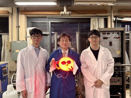
< Photo 1. (from the left) Ph.D. candidate Inki Kim (co-author), Professor SangHyeon Kim (corresponding author), Dr. Joonsup Shim (first author), and Dr. Jinha Lim (co-author) of KAIST School of Electrical Engineering. >
KAIST (represented by President Kwang-Hyung Lee) announced on the 27th of March that a research team led by Professor SangHyeon Kim from the School of Electrical Engineering has developed a mid-infrared photodetector that operates stably at room temperature, marking a major turning point for the commercialization of ultra-compact optical sensors.
The newly developed photodetector utilizes conventional silicon-based CMOS processes, enabling low-cost mass production while maintaining stable operation at room temperature. Notably, the research team successfully demonstrated the real-time detection of carbon dioxide (CO₂) gas using ultra-compact and ultra-thin optical sensors equipped with this photodetector, proving its potential for environmental monitoring and hazardous gas analysis.
Existing mid-infrared photodetectors generally require cooling systems due to high thermal noise at room temperature. These cooling systems increase the size and cost of equipment, making miniaturization and integration into portable devices challenging. Furthermore, conventional mid-infrared photodetectors are incompatible with silicon-based CMOS processes, limiting large-scale production and commercialization.
To address these limitations, the research team developed a waveguide-integrated photodetector using germanium (Ge), a Group IV element like silicon. This approach enables broad-spectrum mid-infrared detection while ensuring stable operation at room temperature.
< Figure 1. Schematic diagram of a room-temperature mid-infrared waveguide-integrated photodetector based on the Ge-on-insulator optical platform proposed in this study (top). Optical microscope image of the integrated photodetector connected with the sensing unit (bottom). >
A waveguide is a structure designed to efficiently guide light along a specific path with minimal loss. To implement various optical functions on a chip (on-chip), the development of waveguide-integrated photodetectors and waveguide-based optical components is essential.
Unlike conventional photodetectors that primarily rely on bandgap absorption principles, this new technology leverages the bolometric effect*, allowing it to detect the entire mid-infrared spectral range. As a result, it can be widely applied to the real-time sensing of various molecular species.
*Bolometric effect: A principle in which light absorption leads to an increase in temperature, causing electrical signals to change accordingly.
The waveguide-integrated mid-infrared photodetector developed by the research team is considered a groundbreaking innovation that overcomes the limitations of existing mid-infrared sensor technologies, including the need for cooling, difficulties in mass production, and high costs.
< Figure 2. Room temperature photoresponse characteristics of the mid-infrared waveguide photodetector proposed in this study (left) and real-time carbon dioxide (CO2) gas sensing results using the photodetector (right). >
This breakthrough technology is expected to be applicable across diverse fields, including environmental monitoring, medical diagnostics, industrial process management, national defense and security, and smart devices. It also paves the way for next-generation mid-infrared sensor advancements.
Professor SangHyeon Kim from KAIST stated, "This research represents a novel approach that overcomes the limitations of existing mid-infrared photodetector technologies and has great potential for practical applications in various fields." He further emphasized, "Since this sensor technology is compatible with CMOS processes, it enables low-cost mass production, making it highly suitable for next-generation environmental monitoring systems and smart manufacturing sites."
< Figure 3. Performance comparison image of a room-temperature mid-infrared waveguide photodetector fabricated with the technology proposed in this study. It achieves the world’s highest performance compared to existing technologies utilizing the Bolometric effect, and is the only solution compatible with CMOS processes. The technology proposed by our research team is characterized by its ability to respond to a wide spectrum of the mid-infrared band without limitations. >
The study, with Dr. Joonsup Shim (currently a postdoctoral researcher at Harvard University) as the first author, was published on March 19, 2025 in the internationally renowned journal Light: Science & Applications (JCR 2.9%, IF=20.6).
(Paper title: “Room-temperature waveguide-integrated photodetector using bolometric effect for mid-infrared spectroscopy applications,” https://doi.org/10.1038/s41377-025-01803-3)
2025.03.27 View 3900
KAIST Innovates Mid-Infrared Photodetectors for Exoplanet Detection, Expanding Applications to Environmental and Medical Fields
NASA’s James Webb Space Telescope (JWST) utilizes mid-infrared spectroscopy to precisely analyze molecular components such as water vapor and sulfur dioxide in exoplanet atmospheres. The key to this analysis, where each molecule exhibits a unique spectral "fingerprint," lies in highly sensitive photodetector technology capable of measuring extremely weak light intensities. Recently, KAIST researchers have developed an innovative photodetector capable of detecting a broad range of mid-infrared spectra, garnering significant attention.
< Photo 1. (from the left) Ph.D. candidate Inki Kim (co-author), Professor SangHyeon Kim (corresponding author), Dr. Joonsup Shim (first author), and Dr. Jinha Lim (co-author) of KAIST School of Electrical Engineering. >
KAIST (represented by President Kwang-Hyung Lee) announced on the 27th of March that a research team led by Professor SangHyeon Kim from the School of Electrical Engineering has developed a mid-infrared photodetector that operates stably at room temperature, marking a major turning point for the commercialization of ultra-compact optical sensors.
The newly developed photodetector utilizes conventional silicon-based CMOS processes, enabling low-cost mass production while maintaining stable operation at room temperature. Notably, the research team successfully demonstrated the real-time detection of carbon dioxide (CO₂) gas using ultra-compact and ultra-thin optical sensors equipped with this photodetector, proving its potential for environmental monitoring and hazardous gas analysis.
Existing mid-infrared photodetectors generally require cooling systems due to high thermal noise at room temperature. These cooling systems increase the size and cost of equipment, making miniaturization and integration into portable devices challenging. Furthermore, conventional mid-infrared photodetectors are incompatible with silicon-based CMOS processes, limiting large-scale production and commercialization.
To address these limitations, the research team developed a waveguide-integrated photodetector using germanium (Ge), a Group IV element like silicon. This approach enables broad-spectrum mid-infrared detection while ensuring stable operation at room temperature.
< Figure 1. Schematic diagram of a room-temperature mid-infrared waveguide-integrated photodetector based on the Ge-on-insulator optical platform proposed in this study (top). Optical microscope image of the integrated photodetector connected with the sensing unit (bottom). >
A waveguide is a structure designed to efficiently guide light along a specific path with minimal loss. To implement various optical functions on a chip (on-chip), the development of waveguide-integrated photodetectors and waveguide-based optical components is essential.
Unlike conventional photodetectors that primarily rely on bandgap absorption principles, this new technology leverages the bolometric effect*, allowing it to detect the entire mid-infrared spectral range. As a result, it can be widely applied to the real-time sensing of various molecular species.
*Bolometric effect: A principle in which light absorption leads to an increase in temperature, causing electrical signals to change accordingly.
The waveguide-integrated mid-infrared photodetector developed by the research team is considered a groundbreaking innovation that overcomes the limitations of existing mid-infrared sensor technologies, including the need for cooling, difficulties in mass production, and high costs.
< Figure 2. Room temperature photoresponse characteristics of the mid-infrared waveguide photodetector proposed in this study (left) and real-time carbon dioxide (CO2) gas sensing results using the photodetector (right). >
This breakthrough technology is expected to be applicable across diverse fields, including environmental monitoring, medical diagnostics, industrial process management, national defense and security, and smart devices. It also paves the way for next-generation mid-infrared sensor advancements.
Professor SangHyeon Kim from KAIST stated, "This research represents a novel approach that overcomes the limitations of existing mid-infrared photodetector technologies and has great potential for practical applications in various fields." He further emphasized, "Since this sensor technology is compatible with CMOS processes, it enables low-cost mass production, making it highly suitable for next-generation environmental monitoring systems and smart manufacturing sites."
< Figure 3. Performance comparison image of a room-temperature mid-infrared waveguide photodetector fabricated with the technology proposed in this study. It achieves the world’s highest performance compared to existing technologies utilizing the Bolometric effect, and is the only solution compatible with CMOS processes. The technology proposed by our research team is characterized by its ability to respond to a wide spectrum of the mid-infrared band without limitations. >
The study, with Dr. Joonsup Shim (currently a postdoctoral researcher at Harvard University) as the first author, was published on March 19, 2025 in the internationally renowned journal Light: Science & Applications (JCR 2.9%, IF=20.6).
(Paper title: “Room-temperature waveguide-integrated photodetector using bolometric effect for mid-infrared spectroscopy applications,” https://doi.org/10.1038/s41377-025-01803-3)
2025.03.27 View 3900 -
 KAIST achieves quantum entanglement essential for quantum error correction
Quantum computing is a technology capable of solving complex problems that classical computers struggle with. To perform accurate computations, quantum computers must correct errors that arise during operations. However, generating the quantum entanglement necessary for quantum error correction has long been considered a major challenge.
< Photo 1. (From left) Students Young-Do Yoon and Chan Roh of the Master's and Doctoral Integrated Program of the Department of Physics poses with Professor Young-Sik Ra and Student Geunhee Gwak of the same program >
KAIST (represented by President Kwang Hyung Lee) announced on the 25th of February that a research team led by Professor Young-Sik Ra from the Department of Physics has successfully implemented a three-dimensional cluster quantum entangled state, a key component for quantum error correction, through experimental demonstration.
Measurement-based quantum computing is an emerging paradigm that implements quantum computations by measuring specially entangled cluster states. The core of this approach lies in the generation of these cluster quantum entangled states, with two-dimensional cluster states commonly used for universal quantum computing.
However, to advance towards fault-tolerant quantum computing, which can correct quantum errors occurring during computations, a more complex three-dimensional cluster state is required. While previous studies have reported the generation of two-dimensional cluster states, experimental implementation of the three-dimensional cluster states necessary for fault-tolerant quantum computing had remained elusive due to the extreme complexity of their entanglement structure.
< Figure 1. (a) Experimental schematic. A pulse laser with a wavelength of 800 nm is converted into a pulse laser with a wavelength of 400 nm through second harmonic generation, and this is incident on a nonlinear crystal (PPKTP) to generate multiple quantum entanglement sources. (b) Generation of a 3D cluster state through optical mode basis change >
The research team overcame this challenge by developing a technique to control femtosecond time-frequency modes, successfully generating a three-dimensional cluster quantum entangled state for the first time.
The team directed a femtosecond laser into a nonlinear crystal, simultaneously generating quantum light sources across multiple frequency modes. (A femtosecond laser is a device that emits ultrashort, high-intensity light pulses.) Using this approach, they successfully created a three-dimensional cluster quantum entangled state.
Professor Young-Sik Ra noted, “This study marks the first successful demonstration of a three-dimensional cluster quantum entangled state, which was previously difficult to achieve with existing technology. This breakthrough is expected to serve as a crucial stepping stone for future research in measurement-based and fault-tolerant quantum computing.”
< Figure 2. Results of 3D cluster state generation. (a) Nullifier measurement of the cluster state. (b) 3D cluster state reconstructed using quantum state tomography. (c) Confirmation of quantum entanglement characteristics of the 3D cluster state >
The study was published online in Nature Photonics on February 24, 2025. The first author is Chan Roh, a Ph.D. candidate in KAIST’s integrated master’s and doctoral program, with Geunhee Gwak and Youngdo Yoon contributing as co-authors. (Paper title: “Generation of Three-Dimensional Cluster Entangled State”, DOI: 10.1038/s41566-025-01631-2)
This research was supported by the National Research Foundation of Korea (Quantum Computing Technology Development Program, Mid-Career Researcher Support Program, and Quantum Simulator for Materials Innovation Program), the Institute for Information & Communications Technology Planning & Evaluation (Quantum Internet Core Technology Program, University ICT Research Center Support Program), and the U.S. Air Force Research Laboratory.
2025.02.25 View 4092
KAIST achieves quantum entanglement essential for quantum error correction
Quantum computing is a technology capable of solving complex problems that classical computers struggle with. To perform accurate computations, quantum computers must correct errors that arise during operations. However, generating the quantum entanglement necessary for quantum error correction has long been considered a major challenge.
< Photo 1. (From left) Students Young-Do Yoon and Chan Roh of the Master's and Doctoral Integrated Program of the Department of Physics poses with Professor Young-Sik Ra and Student Geunhee Gwak of the same program >
KAIST (represented by President Kwang Hyung Lee) announced on the 25th of February that a research team led by Professor Young-Sik Ra from the Department of Physics has successfully implemented a three-dimensional cluster quantum entangled state, a key component for quantum error correction, through experimental demonstration.
Measurement-based quantum computing is an emerging paradigm that implements quantum computations by measuring specially entangled cluster states. The core of this approach lies in the generation of these cluster quantum entangled states, with two-dimensional cluster states commonly used for universal quantum computing.
However, to advance towards fault-tolerant quantum computing, which can correct quantum errors occurring during computations, a more complex three-dimensional cluster state is required. While previous studies have reported the generation of two-dimensional cluster states, experimental implementation of the three-dimensional cluster states necessary for fault-tolerant quantum computing had remained elusive due to the extreme complexity of their entanglement structure.
< Figure 1. (a) Experimental schematic. A pulse laser with a wavelength of 800 nm is converted into a pulse laser with a wavelength of 400 nm through second harmonic generation, and this is incident on a nonlinear crystal (PPKTP) to generate multiple quantum entanglement sources. (b) Generation of a 3D cluster state through optical mode basis change >
The research team overcame this challenge by developing a technique to control femtosecond time-frequency modes, successfully generating a three-dimensional cluster quantum entangled state for the first time.
The team directed a femtosecond laser into a nonlinear crystal, simultaneously generating quantum light sources across multiple frequency modes. (A femtosecond laser is a device that emits ultrashort, high-intensity light pulses.) Using this approach, they successfully created a three-dimensional cluster quantum entangled state.
Professor Young-Sik Ra noted, “This study marks the first successful demonstration of a three-dimensional cluster quantum entangled state, which was previously difficult to achieve with existing technology. This breakthrough is expected to serve as a crucial stepping stone for future research in measurement-based and fault-tolerant quantum computing.”
< Figure 2. Results of 3D cluster state generation. (a) Nullifier measurement of the cluster state. (b) 3D cluster state reconstructed using quantum state tomography. (c) Confirmation of quantum entanglement characteristics of the 3D cluster state >
The study was published online in Nature Photonics on February 24, 2025. The first author is Chan Roh, a Ph.D. candidate in KAIST’s integrated master’s and doctoral program, with Geunhee Gwak and Youngdo Yoon contributing as co-authors. (Paper title: “Generation of Three-Dimensional Cluster Entangled State”, DOI: 10.1038/s41566-025-01631-2)
This research was supported by the National Research Foundation of Korea (Quantum Computing Technology Development Program, Mid-Career Researcher Support Program, and Quantum Simulator for Materials Innovation Program), the Institute for Information & Communications Technology Planning & Evaluation (Quantum Internet Core Technology Program, University ICT Research Center Support Program), and the U.S. Air Force Research Laboratory.
2025.02.25 View 4092 -
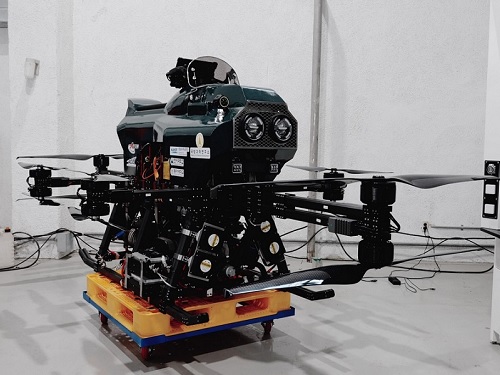 KAIST develops ‘Hoverbike’ to roam the future skies
< Photo 1. A group photo of the research team >
Hoverbike is a kind of next-generation mobility that can complement the existing transportation system and can be used as an air transportation means without traffic congestion through high-weight payloads and long-distance flights. It is expected that domestic researchers will contribute to the development of the domestic PAV* and UAM markets by developing a domestically developed manned/unmanned hybrid aircraft that escapes dependence on foreign technology through the development of a high-performance hoverbike.
*PAV: Personal Aerial Vehicle. It is a key element of future urban air mobility (UAM, Urban Air Mobility) and constitutes an important part of the next-generation transportation system.
KAIST (President Kwang-Hyung Lee) announced on the 27th of December that the research team of Professor Hyochoong Bang of the Department of Aerospace Engineering successfully developed the core technology of a highly reliable multipurpose vertical takeoff and landing hoverbike that can be operated by both manned and unmanned vehicles.
This research was participated by the research teams of Professor Jae-Hung Han, Professor Ji-yun Lee, Professor Jae-myung Ahn, Professor Han-Lim Choi, and Professor Chang-Hun Lee of the Department of Aerospace Engineering at KAIST, Professor Dongjin Lee of the Department of Unmanned Aerial Vehicles at Hanseo University, and Professor Jong-Oh Park of the Department of Electronics Engineering at Dong-A University.
The research team secured key technologies related to the optimal design of a multipurpose aircraft, hybrid propulsion system, highly reliable precision navigation and flight control system, autonomous flight, and fault detection for the development of a high-performance hoverbike.
< Figure 1. Key features of high-reliability multi-purpose hoverbike >
The hoverbike platform introduced a gasoline engine-based hybrid system to overcome the shortcomings of battery-based drones, achieving approximately 60% better performance and maximum payload weight compared to overseas technology levels. Through this, it is expected to be utilized in various fields such as emergency supply delivery, logistics, and rescue activities for civilian use, and military transport and mission support for military use.
The navigation system was applied by implementing multi-sensor fusion technology based on DGPS/INS* to enable stable flight even in environments without GPS or with weak signals using high-reliability precision navigation technology.
*DGPS/INS: Navigation solution combining high accuracy of Differential GPS (DGPS) and Inertial Navigation System (INS)
In addition, high-reliability flight control technology was developed to enable reliable maneuvering even under external factors such as payload and wind, and model uncertainty, and fault detection technology was also developed.
A guidance technique to automatically land on a helipad after selecting a safe automatic landing area by configuring a high-reliability autonomous flight system was implemented with high accuracy. Stable operation is possible even in complex environments through obstacle avoidance and automatic landing autonomous flight technology.
< Figure 2. Hoverbike prototype model >
Professor Hyochoong Bang, the research director, emphasized, “We have proven the high practicality of the hoverbike in various environments through high-reliability flight control and precision navigation technology.” He added, “The hoverbike is a promising research result that can not only provide a major path leading to PAVs and future aircraft, but also surpass existing drone technology by several levels. This achievement is even more meaningful because it is the result of five years of effort by eight joint research teams, including the project’s practitioners, PhD students Kwangwoo Jang and Hyungjoo Ahn.”
This study aims to secure core technologies for manned/unmanned multipurpose hoverbikes that can be utilized as new concept aircraft in the defense and civilian sectors. It started as the Defense Acquisition Program Administration’s Defense Technology for Future Challenge Research and Development Project in 2019 and was completed in 2024 under the management of the Agency for Defense Development. It is scheduled to be exhibited for the first time at the 2025 Drone Show Korea (DSK2025), which will be held at BEXCO in Busan from February 26 to 28, 2025.
2024.12.27 View 5972
KAIST develops ‘Hoverbike’ to roam the future skies
< Photo 1. A group photo of the research team >
Hoverbike is a kind of next-generation mobility that can complement the existing transportation system and can be used as an air transportation means without traffic congestion through high-weight payloads and long-distance flights. It is expected that domestic researchers will contribute to the development of the domestic PAV* and UAM markets by developing a domestically developed manned/unmanned hybrid aircraft that escapes dependence on foreign technology through the development of a high-performance hoverbike.
*PAV: Personal Aerial Vehicle. It is a key element of future urban air mobility (UAM, Urban Air Mobility) and constitutes an important part of the next-generation transportation system.
KAIST (President Kwang-Hyung Lee) announced on the 27th of December that the research team of Professor Hyochoong Bang of the Department of Aerospace Engineering successfully developed the core technology of a highly reliable multipurpose vertical takeoff and landing hoverbike that can be operated by both manned and unmanned vehicles.
This research was participated by the research teams of Professor Jae-Hung Han, Professor Ji-yun Lee, Professor Jae-myung Ahn, Professor Han-Lim Choi, and Professor Chang-Hun Lee of the Department of Aerospace Engineering at KAIST, Professor Dongjin Lee of the Department of Unmanned Aerial Vehicles at Hanseo University, and Professor Jong-Oh Park of the Department of Electronics Engineering at Dong-A University.
The research team secured key technologies related to the optimal design of a multipurpose aircraft, hybrid propulsion system, highly reliable precision navigation and flight control system, autonomous flight, and fault detection for the development of a high-performance hoverbike.
< Figure 1. Key features of high-reliability multi-purpose hoverbike >
The hoverbike platform introduced a gasoline engine-based hybrid system to overcome the shortcomings of battery-based drones, achieving approximately 60% better performance and maximum payload weight compared to overseas technology levels. Through this, it is expected to be utilized in various fields such as emergency supply delivery, logistics, and rescue activities for civilian use, and military transport and mission support for military use.
The navigation system was applied by implementing multi-sensor fusion technology based on DGPS/INS* to enable stable flight even in environments without GPS or with weak signals using high-reliability precision navigation technology.
*DGPS/INS: Navigation solution combining high accuracy of Differential GPS (DGPS) and Inertial Navigation System (INS)
In addition, high-reliability flight control technology was developed to enable reliable maneuvering even under external factors such as payload and wind, and model uncertainty, and fault detection technology was also developed.
A guidance technique to automatically land on a helipad after selecting a safe automatic landing area by configuring a high-reliability autonomous flight system was implemented with high accuracy. Stable operation is possible even in complex environments through obstacle avoidance and automatic landing autonomous flight technology.
< Figure 2. Hoverbike prototype model >
Professor Hyochoong Bang, the research director, emphasized, “We have proven the high practicality of the hoverbike in various environments through high-reliability flight control and precision navigation technology.” He added, “The hoverbike is a promising research result that can not only provide a major path leading to PAVs and future aircraft, but also surpass existing drone technology by several levels. This achievement is even more meaningful because it is the result of five years of effort by eight joint research teams, including the project’s practitioners, PhD students Kwangwoo Jang and Hyungjoo Ahn.”
This study aims to secure core technologies for manned/unmanned multipurpose hoverbikes that can be utilized as new concept aircraft in the defense and civilian sectors. It started as the Defense Acquisition Program Administration’s Defense Technology for Future Challenge Research and Development Project in 2019 and was completed in 2024 under the management of the Agency for Defense Development. It is scheduled to be exhibited for the first time at the 2025 Drone Show Korea (DSK2025), which will be held at BEXCO in Busan from February 26 to 28, 2025.
2024.12.27 View 5972 -
 KAIST Secures Core Technology for Ultra-High-Resolution Image Sensors
A joint research team from Korea and the United States has developed next-generation, high-resolution image sensor technology with higher power efficiency and a smaller size compared to existing sensors. Notably, they have secured foundational technology for ultra-high-resolution shortwave infrared (SWIR) image sensors, an area currently dominated by Sony, paving the way for future market entry.
KAIST (represented by President Kwang Hyung Lee) announced on the 20th of November that a research team led by Professor SangHyeon Kim from the School of Electrical Engineering, in collaboration with Inha University and Yale University in the U.S., has developed an ultra-thin broadband photodiode (PD), marking a significant breakthrough in high-performance image sensor technology.
This research drastically improves the trade-off between the absorption layer thickness and quantum efficiency found in conventional photodiode technology. Specifically, it achieved high quantum efficiency of over 70% even in an absorption layer thinner than one micrometer (μm), reducing the thickness of the absorption layer by approximately 70% compared to existing technologies.
A thinner absorption layer simplifies pixel processing, allowing for higher resolution and smoother carrier diffusion, which is advantageous for light carrier acquisition while also reducing the cost. However, a fundamental issue with thinner absorption layers is the reduced absorption of long-wavelength light.
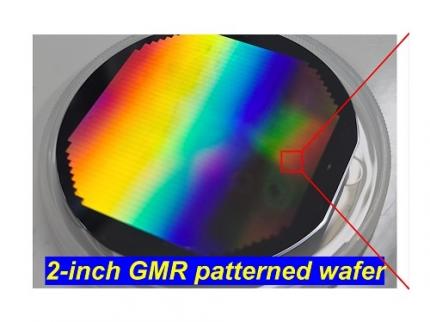
< Figure 1. Schematic diagram of the InGaAs photodiode image sensor integrated on the Guided-Mode Resonance (GMR) structure proposed in this study (left), a photograph of the fabricated wafer, and a scanning electron microscope (SEM) image of the periodic patterns (right) >
The research team introduced a guided-mode resonance (GMR) structure* that enables high-efficiency light absorption across a wide spectral range from 400 nanometers (nm) to 1,700 nanometers (nm). This wavelength range includes not only visible light but also light the SWIR region, making it valuable for various industrial applications.
*Guided-Mode Resonance (GMR) Structure: A concept used in electromagnetics, a phenomenon in which a specific (light) wave resonates (forming a strong electric/magnetic field) at a specific wavelength. Since energy is maximized under these conditions, it has been used to increase antenna or radar efficiency.
The improved performance in the SWIR region is expected to play a significant role in developing next-generation image sensors with increasingly high resolutions. The GMR structure, in particular, holds potential for further enhancing resolution and other performance metrics through hybrid integration and monolithic 3D integration with complementary metal-oxide-semiconductor (CMOS)-based readout integrated circuits (ROIC).
< Figure 2. Benchmark for state-of-the-art InGaAs-based SWIR pixels with simulated EQE lines as a function of TAL variation. Performance is maintained while reducing the absorption layer thickness from 2.1 micrometers or more to 1 micrometer or less while reducing it by 50% to 70% >
The research team has significantly enhanced international competitiveness in low-power devices and ultra-high-resolution imaging technology, opening up possibilities for applications in digital cameras, security systems, medical and industrial image sensors, as well as future ultra-high-resolution sensors for autonomous driving, aerospace, and satellite observation.
Professor Sang Hyun Kim, the lead researcher, commented, “This research demonstrates that significantly higher performance than existing technologies can be achieved even with ultra-thin absorption layers.”
< Figure 3. Top optical microscope image and cross-sectional scanning electron microscope image of the InGaAs photodiode image sensor fabricated on the GMR structure (left). Improved quantum efficiency performance of the ultra-thin image sensor (red) fabricated with the technology proposed in this study (right) >
The results of this research were published on 15th of November, in the prestigious international journal Light: Science & Applications (JCR 2.9%, IF=20.6), with Professor Dae-Myung Geum of Inha University (formerly a KAIST postdoctoral researcher) and Dr. Jinha Lim (currently a postdoctoral researcher at Yale University) as co-first authors. (Paper title: “Highly-efficient (>70%) and Wide-spectral (400 nm -1700 nm) sub-micron-thick InGaAs photodiodes for future high-resolution image sensors”)
This study was supported by the National Research Foundation of Korea.
2024.11.22 View 6858
KAIST Secures Core Technology for Ultra-High-Resolution Image Sensors
A joint research team from Korea and the United States has developed next-generation, high-resolution image sensor technology with higher power efficiency and a smaller size compared to existing sensors. Notably, they have secured foundational technology for ultra-high-resolution shortwave infrared (SWIR) image sensors, an area currently dominated by Sony, paving the way for future market entry.
KAIST (represented by President Kwang Hyung Lee) announced on the 20th of November that a research team led by Professor SangHyeon Kim from the School of Electrical Engineering, in collaboration with Inha University and Yale University in the U.S., has developed an ultra-thin broadband photodiode (PD), marking a significant breakthrough in high-performance image sensor technology.
This research drastically improves the trade-off between the absorption layer thickness and quantum efficiency found in conventional photodiode technology. Specifically, it achieved high quantum efficiency of over 70% even in an absorption layer thinner than one micrometer (μm), reducing the thickness of the absorption layer by approximately 70% compared to existing technologies.
A thinner absorption layer simplifies pixel processing, allowing for higher resolution and smoother carrier diffusion, which is advantageous for light carrier acquisition while also reducing the cost. However, a fundamental issue with thinner absorption layers is the reduced absorption of long-wavelength light.
< Figure 1. Schematic diagram of the InGaAs photodiode image sensor integrated on the Guided-Mode Resonance (GMR) structure proposed in this study (left), a photograph of the fabricated wafer, and a scanning electron microscope (SEM) image of the periodic patterns (right) >
The research team introduced a guided-mode resonance (GMR) structure* that enables high-efficiency light absorption across a wide spectral range from 400 nanometers (nm) to 1,700 nanometers (nm). This wavelength range includes not only visible light but also light the SWIR region, making it valuable for various industrial applications.
*Guided-Mode Resonance (GMR) Structure: A concept used in electromagnetics, a phenomenon in which a specific (light) wave resonates (forming a strong electric/magnetic field) at a specific wavelength. Since energy is maximized under these conditions, it has been used to increase antenna or radar efficiency.
The improved performance in the SWIR region is expected to play a significant role in developing next-generation image sensors with increasingly high resolutions. The GMR structure, in particular, holds potential for further enhancing resolution and other performance metrics through hybrid integration and monolithic 3D integration with complementary metal-oxide-semiconductor (CMOS)-based readout integrated circuits (ROIC).
< Figure 2. Benchmark for state-of-the-art InGaAs-based SWIR pixels with simulated EQE lines as a function of TAL variation. Performance is maintained while reducing the absorption layer thickness from 2.1 micrometers or more to 1 micrometer or less while reducing it by 50% to 70% >
The research team has significantly enhanced international competitiveness in low-power devices and ultra-high-resolution imaging technology, opening up possibilities for applications in digital cameras, security systems, medical and industrial image sensors, as well as future ultra-high-resolution sensors for autonomous driving, aerospace, and satellite observation.
Professor Sang Hyun Kim, the lead researcher, commented, “This research demonstrates that significantly higher performance than existing technologies can be achieved even with ultra-thin absorption layers.”
< Figure 3. Top optical microscope image and cross-sectional scanning electron microscope image of the InGaAs photodiode image sensor fabricated on the GMR structure (left). Improved quantum efficiency performance of the ultra-thin image sensor (red) fabricated with the technology proposed in this study (right) >
The results of this research were published on 15th of November, in the prestigious international journal Light: Science & Applications (JCR 2.9%, IF=20.6), with Professor Dae-Myung Geum of Inha University (formerly a KAIST postdoctoral researcher) and Dr. Jinha Lim (currently a postdoctoral researcher at Yale University) as co-first authors. (Paper title: “Highly-efficient (>70%) and Wide-spectral (400 nm -1700 nm) sub-micron-thick InGaAs photodiodes for future high-resolution image sensors”)
This study was supported by the National Research Foundation of Korea.
2024.11.22 View 6858 -
 A KAIST Team Develops Face-Conforming LED Mask Showing 340% Improved Efficacy in Deep Skin Elasticity
- A KAIST research team led by Professor Keon Jae Lee has developed a deep skin-stimulating LED mask which has been verified in clinical trials to improve dermis elasticity by 340%.
< Figure 1. Overall concept of face-fit surface-lighting micro-LEDs (FSLED) mask. a. Optical image of the FSLED mask showing uniform surface-lighting. schematic illustration of the FSLED mask. The 2D to 3D transformation procedure b. Difference in cosmetic effect on deep skin elasticity, wrinkles, and sagging between FSLED mask and CLED mask. (improvement percentage in eight weeks) >
Conventional LED masks, with their rigid design, fail to conform closely to the skin's contours. This limitation causes substantial light reflection, with up to 90% reflected over a distance of 2 cm, reducing light penetration and limiting stimulation of the deep skin layers essential for effective skin rejuvenation.
To address these challenges, Professor Lee's team developed a face-conforming surface lighting micro-LED (FSLED) mask, which can provide uniform photostimulation to the dermis. The key technology lies in the mask's ability to deliver uniform light to deep skin tissues while maintaining a conformal skin attachment. This is achieved through a 3D origami structure, integrated with 3,770 micro-LEDs and flexible surface light-diffusion layer, minimizing the gaps between the light source and the skin.
In clinical trials involving 33 participants, the FSLED mask demonstrated a 340% improvement in deep skin elasticity compared to conventional LED masks, proving its efficacy in significantly reducing skin wrinkles, sagging and aging.
Professor Keon Jae Lee said, “The FSLED mask provides cosmetic benefits to the entire facial dermis without the side effects of low-temperature burns, making home-care anti-aging treatment that enhances the quality of human life possible. The product is being manufactured by Fronics, KAIST startup company, and will be distributed globally through Amorepacific's network, with sales starting in November.”
This result titled “Clinical Validation of Face-fit Surface-lighting Micro Light-emitting Diode Mask for Skin Anti-aging Treatment”, in which Min Seo Kim, a student of the Master-Doctorate integrated program, and Jaehun An, a Ph.D. candidate, in the Department of Materials Science and Engineering of KAIST, took part as co-first authors, was published in Advanced Materials on October 22nd, 2024 (DOI: 10.1002/adma.202411651).
Introductory Video: Face-conforming surface LED mask for skin anti-aging ( https://www.youtube.com/watch?v=kSccLwx8N_w )
2024.10.29 View 8675
A KAIST Team Develops Face-Conforming LED Mask Showing 340% Improved Efficacy in Deep Skin Elasticity
- A KAIST research team led by Professor Keon Jae Lee has developed a deep skin-stimulating LED mask which has been verified in clinical trials to improve dermis elasticity by 340%.
< Figure 1. Overall concept of face-fit surface-lighting micro-LEDs (FSLED) mask. a. Optical image of the FSLED mask showing uniform surface-lighting. schematic illustration of the FSLED mask. The 2D to 3D transformation procedure b. Difference in cosmetic effect on deep skin elasticity, wrinkles, and sagging between FSLED mask and CLED mask. (improvement percentage in eight weeks) >
Conventional LED masks, with their rigid design, fail to conform closely to the skin's contours. This limitation causes substantial light reflection, with up to 90% reflected over a distance of 2 cm, reducing light penetration and limiting stimulation of the deep skin layers essential for effective skin rejuvenation.
To address these challenges, Professor Lee's team developed a face-conforming surface lighting micro-LED (FSLED) mask, which can provide uniform photostimulation to the dermis. The key technology lies in the mask's ability to deliver uniform light to deep skin tissues while maintaining a conformal skin attachment. This is achieved through a 3D origami structure, integrated with 3,770 micro-LEDs and flexible surface light-diffusion layer, minimizing the gaps between the light source and the skin.
In clinical trials involving 33 participants, the FSLED mask demonstrated a 340% improvement in deep skin elasticity compared to conventional LED masks, proving its efficacy in significantly reducing skin wrinkles, sagging and aging.
Professor Keon Jae Lee said, “The FSLED mask provides cosmetic benefits to the entire facial dermis without the side effects of low-temperature burns, making home-care anti-aging treatment that enhances the quality of human life possible. The product is being manufactured by Fronics, KAIST startup company, and will be distributed globally through Amorepacific's network, with sales starting in November.”
This result titled “Clinical Validation of Face-fit Surface-lighting Micro Light-emitting Diode Mask for Skin Anti-aging Treatment”, in which Min Seo Kim, a student of the Master-Doctorate integrated program, and Jaehun An, a Ph.D. candidate, in the Department of Materials Science and Engineering of KAIST, took part as co-first authors, was published in Advanced Materials on October 22nd, 2024 (DOI: 10.1002/adma.202411651).
Introductory Video: Face-conforming surface LED mask for skin anti-aging ( https://www.youtube.com/watch?v=kSccLwx8N_w )
2024.10.29 View 8675 -
 KAIST Changes the Paradigm of Drug Discovery with World's First Atomic Editing
In pioneering drug development, the new technology that enables the easy and rapid editing of key atoms responsible for drug efficacy has been regarded as a fundamental and "dream" technology, revolutionizing the process of discovering potential drug candidates. KAIST researchers have become the first in the world to successfully develop single-atom editing technology that maximizes drug efficacy.
On October 8th, KAIST (represented by President Kwang-Hyung Lee) announced that Professor Yoonsu Park’s research team from the Department of Chemistry successfully developed technology that enables the easy editing and correction of oxygen atoms in furan compounds into nitrogen atoms, directly converting them into pyrrole frameworks, which are widely used in pharmaceuticals.
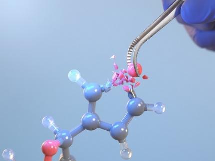
< Image. Conceptual image illustrating the main idea of the research >
This research was published in the prestigious scientific journal Science on October 3rd under the title "Photocatalytic Furan-to-Pyrrole Conversion."
Many drugs have complex chemical structures, but their efficacy is often determined by a single critical atom. Atoms like oxygen and nitrogen play a central role in enhancing the pharmacological effects of these drugs, particularly against viruses.
This phenomenon, where the introduction of specific atoms into a drug molecule dramatically affects its efficacy, is known as the "Single Atom Effect." In leading-edge drug development, discovering atoms that maximize drug efficacy is key.
However, evaluating the Single Atom Effect has traditionally required multi-step, costly synthesis processes, as it has been difficult to selectively edit single atoms within stable ring structures containing oxygen or nitrogen.
Professor Park’s team overcame this challenge by introducing a photocatalyst that uses light energy. They developed a photocatalyst that acts as a “molecular scissor,” freely cutting and attaching five-membered rings, enabling single-atom editing at room temperature and atmospheric pressure—a world first.
The team discovered a new reaction mechanism in which the excited molecular scissor removes oxygen from furan via single-electron oxidation and then sequentially adds a nitrogen atom.
Donghyeon Kim and Jaehyun You, the study's first authors and candidates in KAIST’s integrated master's and doctoral program in the Department of Chemistry, explained that this technique offers high versatility by utilizing light energy to replace harsh conditions. They further noted that the technology enables selective editing, even when applied to complex natural products or pharmaceuticals. Professor Yoonsu Park, who led the research, remarked, "This breakthrough, which allows for the selective editing of five-membered organic ring structures, will open new doors for building libraries of drug candidates, a key challenge in pharmaceuticals. I hope this foundational technology will be used to revolutionize the drug development process."
The significance of this research was highlighted in the Perspective section of Science, a feature where a peer scientist of prominence outside of the project group provides commentary on an impactful research.
This research was supported by the National Research Foundation of Korea’s Creative Research Program, the Cross-Generation Collaborative Lab Project at KAIST, and the POSCO Science Fellowship of the POSCO TJ Park Foundation.
2024.10.11 View 6505
KAIST Changes the Paradigm of Drug Discovery with World's First Atomic Editing
In pioneering drug development, the new technology that enables the easy and rapid editing of key atoms responsible for drug efficacy has been regarded as a fundamental and "dream" technology, revolutionizing the process of discovering potential drug candidates. KAIST researchers have become the first in the world to successfully develop single-atom editing technology that maximizes drug efficacy.
On October 8th, KAIST (represented by President Kwang-Hyung Lee) announced that Professor Yoonsu Park’s research team from the Department of Chemistry successfully developed technology that enables the easy editing and correction of oxygen atoms in furan compounds into nitrogen atoms, directly converting them into pyrrole frameworks, which are widely used in pharmaceuticals.
< Image. Conceptual image illustrating the main idea of the research >
This research was published in the prestigious scientific journal Science on October 3rd under the title "Photocatalytic Furan-to-Pyrrole Conversion."
Many drugs have complex chemical structures, but their efficacy is often determined by a single critical atom. Atoms like oxygen and nitrogen play a central role in enhancing the pharmacological effects of these drugs, particularly against viruses.
This phenomenon, where the introduction of specific atoms into a drug molecule dramatically affects its efficacy, is known as the "Single Atom Effect." In leading-edge drug development, discovering atoms that maximize drug efficacy is key.
However, evaluating the Single Atom Effect has traditionally required multi-step, costly synthesis processes, as it has been difficult to selectively edit single atoms within stable ring structures containing oxygen or nitrogen.
Professor Park’s team overcame this challenge by introducing a photocatalyst that uses light energy. They developed a photocatalyst that acts as a “molecular scissor,” freely cutting and attaching five-membered rings, enabling single-atom editing at room temperature and atmospheric pressure—a world first.
The team discovered a new reaction mechanism in which the excited molecular scissor removes oxygen from furan via single-electron oxidation and then sequentially adds a nitrogen atom.
Donghyeon Kim and Jaehyun You, the study's first authors and candidates in KAIST’s integrated master's and doctoral program in the Department of Chemistry, explained that this technique offers high versatility by utilizing light energy to replace harsh conditions. They further noted that the technology enables selective editing, even when applied to complex natural products or pharmaceuticals. Professor Yoonsu Park, who led the research, remarked, "This breakthrough, which allows for the selective editing of five-membered organic ring structures, will open new doors for building libraries of drug candidates, a key challenge in pharmaceuticals. I hope this foundational technology will be used to revolutionize the drug development process."
The significance of this research was highlighted in the Perspective section of Science, a feature where a peer scientist of prominence outside of the project group provides commentary on an impactful research.
This research was supported by the National Research Foundation of Korea’s Creative Research Program, the Cross-Generation Collaborative Lab Project at KAIST, and the POSCO Science Fellowship of the POSCO TJ Park Foundation.
2024.10.11 View 6505 -
 Professor Jimin Park and Dr. Inho Kim join the ranks of the 2024 "35 Innovators Under 35" by the MIT Technology Review
< (From left) Professor Jimin Park of the Department of Chemical and Biomolecular Engineering and Dr. Inho Kim, a graduate of the Department of Materials Science and Engineering >
KAIST (represented by President Kwang-Hyung Lee) announced on the 13th of September that Professor Jimin Park from KAIST’s Department of Chemical and Biomolecular Engineering and Dr. Inho Kim, a graduate from the Department of Materials Science and Engineering (currently a postdoctoral researcher at Caltech), were selected by the MIT Technology Review as the 2024 "35 Innovators Under 35”.
The MIT Technology Review, first published in 1899 by the Massachusetts Institute of Technology, is the world’s oldest and most influential magazine on science and technology, offering in-depth analysis across various technology fields, expanding knowledge and providing insights into cutting-edge technology trends.
Since 1999, the magazine has annually named 35 innovators under the age of 35, recognizing young talents making groundbreaking contributions in modern technology fields. The recognition is globally considered a prestigious honor and a dream for young researchers in the science and technology community.
< Image 1. Introduction for Professor Jimin Park at the Meet 35 Innovators Under 35 Summit 2024 >
Professor Jimin Park is developing next-generation bio-interfaces that link artificial materials with living organisms, and is engaged in advanced research in areas such as digital healthcare and carbon-neutral compound manufacturing technologies. In 2014, Professor Park was also recognized as one of the ‘Asia Pacific Innovators Under 35’ by the MIT Technology Review, which highlights young scientists in the Asia-Pacific region.
Professor Park responded, “It’s a great honor to be named as one of the young innovators by the MIT Technology Review, a symbol of innovation with a long history. I will continue to pursue challenging, interdisciplinary research to develop next-generation interfaces that seamlessly connect artificial materials and living organisms, from atomic to system levels.”
< Image 2. Introduction for Dr. Inho Kim as the 2024 Innovator of Materials Science for 35 Innovators Under 35 >
Dr. Inho Kim, who earned his PhD from KAIST in 2020 under the supervision of Professor Sang Ouk Kim from the Department of Materials Science and Engineering, recently succeeded in developing a new artificial muscle using composite fibers. This new material is considered the most human-like muscle ever reported in scientific literature, while also being 17 times stronger than natural human muscle.
Dr. Kim is researching the application of artificial muscle fibers in next-generation wearable assistive devices that move more naturally, like humans or animals, noting that the fibers are lightweight, flexible, and exhibit conductivity during contraction, enabling real-time feedback. Recognized for this potential, Dr. Inho Kim was named one of the '35 Innovators Under 35' this year, making him the first researcher to win the honor with the research conducted at KAIST and a PhD earned from Korea.
Dr. Kim stated, “I aim to develop robots using these new materials that can replace today’s expensive and heavy exoskeleton suits by eliminating motors and rigid frames. This will significantly reduce costs and allow for better customization, making cutting-edge technology more accessible to those who need it most, like children with cerebral palsy.”
2024.09.13 View 9316
Professor Jimin Park and Dr. Inho Kim join the ranks of the 2024 "35 Innovators Under 35" by the MIT Technology Review
< (From left) Professor Jimin Park of the Department of Chemical and Biomolecular Engineering and Dr. Inho Kim, a graduate of the Department of Materials Science and Engineering >
KAIST (represented by President Kwang-Hyung Lee) announced on the 13th of September that Professor Jimin Park from KAIST’s Department of Chemical and Biomolecular Engineering and Dr. Inho Kim, a graduate from the Department of Materials Science and Engineering (currently a postdoctoral researcher at Caltech), were selected by the MIT Technology Review as the 2024 "35 Innovators Under 35”.
The MIT Technology Review, first published in 1899 by the Massachusetts Institute of Technology, is the world’s oldest and most influential magazine on science and technology, offering in-depth analysis across various technology fields, expanding knowledge and providing insights into cutting-edge technology trends.
Since 1999, the magazine has annually named 35 innovators under the age of 35, recognizing young talents making groundbreaking contributions in modern technology fields. The recognition is globally considered a prestigious honor and a dream for young researchers in the science and technology community.
< Image 1. Introduction for Professor Jimin Park at the Meet 35 Innovators Under 35 Summit 2024 >
Professor Jimin Park is developing next-generation bio-interfaces that link artificial materials with living organisms, and is engaged in advanced research in areas such as digital healthcare and carbon-neutral compound manufacturing technologies. In 2014, Professor Park was also recognized as one of the ‘Asia Pacific Innovators Under 35’ by the MIT Technology Review, which highlights young scientists in the Asia-Pacific region.
Professor Park responded, “It’s a great honor to be named as one of the young innovators by the MIT Technology Review, a symbol of innovation with a long history. I will continue to pursue challenging, interdisciplinary research to develop next-generation interfaces that seamlessly connect artificial materials and living organisms, from atomic to system levels.”
< Image 2. Introduction for Dr. Inho Kim as the 2024 Innovator of Materials Science for 35 Innovators Under 35 >
Dr. Inho Kim, who earned his PhD from KAIST in 2020 under the supervision of Professor Sang Ouk Kim from the Department of Materials Science and Engineering, recently succeeded in developing a new artificial muscle using composite fibers. This new material is considered the most human-like muscle ever reported in scientific literature, while also being 17 times stronger than natural human muscle.
Dr. Kim is researching the application of artificial muscle fibers in next-generation wearable assistive devices that move more naturally, like humans or animals, noting that the fibers are lightweight, flexible, and exhibit conductivity during contraction, enabling real-time feedback. Recognized for this potential, Dr. Inho Kim was named one of the '35 Innovators Under 35' this year, making him the first researcher to win the honor with the research conducted at KAIST and a PhD earned from Korea.
Dr. Kim stated, “I aim to develop robots using these new materials that can replace today’s expensive and heavy exoskeleton suits by eliminating motors and rigid frames. This will significantly reduce costs and allow for better customization, making cutting-edge technology more accessible to those who need it most, like children with cerebral palsy.”
2024.09.13 View 9316 -
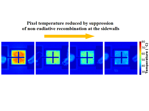 KAIST researchers devises a technology to utilize ultrahigh-resolution micro-LED with 40% reduced self-generated heat
In the digitized modern life, various forms of future displays, such as wearable and rollable displays are required. More and more people are wanting to connect to the virtual world whenever and wherever with the use of their smartglasses or smartwatches. Even further, we’ve been hearing about medical diagnosis kit on a shirt and a theatre-hat. However, it is not quite here in our hands yet due to technical limitations of being unable to fit as many pixels as a limited surface area of a glasses while keeping the power consumption at the a level that a hand held battery can supply, all the while the resolution of 4K+ is needed in order to perfectly immerse the users into the augmented or virtual reality through a wireless smartglasses or whatever the device.
KAIST (President Kwang Hyung Lee) announced on the 22nd that Professor Sang Hyeon Kim's research team of the Department of Electrical and Electronic Engineering re-examined the phenomenon of efficiency degradation of micro-LEDs with pixels in a size of micrometers (μm, one millionth of a meter) and found that it was possible to fundamentally resolve the problem by the use of epitaxial structure engineering.
Epitaxy refers to the process of stacking gallium nitride crystals that are used as a light emitting body on top of an ultrapure silicon or sapphire substrate used for μLEDs as a medium.
μLED is being actively studied because it has the advantages of superior brightness, contrast ratio, and lifespan compared to OLED. In 2018, Samsung Electronics commercialized a product equipped with μLED called 'The Wall'. And there is a prospect that Apple may be launching a μLED-mounted product in 2025.
In order to manufacture μLEDs, pixels are formed by cutting the epitaxial structure grown on a wafer into a cylinder or cuboid shape through an etching process, and this etching process is accompanied by a plasma-based process. However, these plasmas generate defects on the side of the pixel during the pixel formation process.
Therefore, as the pixel size becomes smaller and the resolution increases, the ratio of the surface area to the volume of the pixel increases, and defects on the side of the device that occur during processing further reduce the device efficiency of the μLED. Accordingly, a considerable amount of research has been conducted on mitigating or removing sidewall defects, but this method has a limit to the degree of improvement as it must be done at the post-processing stage after the grown of the epitaxial structure is finished.
The research team identified that there is a difference in the current moving to the sidewall of the μLED depending on the epitaxial structure during μLED device operation, and based on the findings, the team built a structure that is not sensitive to sidewall defects to solve the problem of reduced efficiency due to miniaturization of μLED devices. In addition, the proposed structure reduced the self-generated heat while the device was running by about 40% compared to the existing structure, which is also of great significance in commercialization of ultrahigh-resolution μLED displays.
This study, which was led by Woo Jin Baek of Professor Sang Hyeon Kim's research team at the KAIST School of Electrical and Electronic Engineering as the first author with guidance by Professor Sang Hyeon Kim and Professor Dae-Myeong Geum of the Chungbuk National University (who was with the team as a postdoctoral researcher at the time) as corresponding authors, was published in the international journal, 'Nature Communications' on March 17th. (Title of the paper: Ultra-low-current driven InGaN blue micro light-emitting diodes for electrically efficient and self-heating relaxed microdisplay).
Professor Sang Hyeon Kim said, "This technological development has great meaning in identifying the cause of the drop in efficiency, which was an obstacle to miniaturization of μLED, and solving it with the design of the epitaxial structure.“ He added, ”We are looking forward to it being used in manufacturing of ultrahigh-resolution displays in the future."
This research was carried out with the support of the Samsung Future Technology Incubation Center.
Figure 1. Image of electroluminescence distribution of μLEDs fabricated from epitaxial structures with quantum barriers of different thicknesses while the current is running
Figure 2. Thermal distribution images of devices fabricated with different epitaxial structures under the same amount of light.
Figure 3. Normalized external quantum efficiency of the device fabricated with the optimized epitaxial structure by sizes.
2023.03.23 View 9006
KAIST researchers devises a technology to utilize ultrahigh-resolution micro-LED with 40% reduced self-generated heat
In the digitized modern life, various forms of future displays, such as wearable and rollable displays are required. More and more people are wanting to connect to the virtual world whenever and wherever with the use of their smartglasses or smartwatches. Even further, we’ve been hearing about medical diagnosis kit on a shirt and a theatre-hat. However, it is not quite here in our hands yet due to technical limitations of being unable to fit as many pixels as a limited surface area of a glasses while keeping the power consumption at the a level that a hand held battery can supply, all the while the resolution of 4K+ is needed in order to perfectly immerse the users into the augmented or virtual reality through a wireless smartglasses or whatever the device.
KAIST (President Kwang Hyung Lee) announced on the 22nd that Professor Sang Hyeon Kim's research team of the Department of Electrical and Electronic Engineering re-examined the phenomenon of efficiency degradation of micro-LEDs with pixels in a size of micrometers (μm, one millionth of a meter) and found that it was possible to fundamentally resolve the problem by the use of epitaxial structure engineering.
Epitaxy refers to the process of stacking gallium nitride crystals that are used as a light emitting body on top of an ultrapure silicon or sapphire substrate used for μLEDs as a medium.
μLED is being actively studied because it has the advantages of superior brightness, contrast ratio, and lifespan compared to OLED. In 2018, Samsung Electronics commercialized a product equipped with μLED called 'The Wall'. And there is a prospect that Apple may be launching a μLED-mounted product in 2025.
In order to manufacture μLEDs, pixels are formed by cutting the epitaxial structure grown on a wafer into a cylinder or cuboid shape through an etching process, and this etching process is accompanied by a plasma-based process. However, these plasmas generate defects on the side of the pixel during the pixel formation process.
Therefore, as the pixel size becomes smaller and the resolution increases, the ratio of the surface area to the volume of the pixel increases, and defects on the side of the device that occur during processing further reduce the device efficiency of the μLED. Accordingly, a considerable amount of research has been conducted on mitigating or removing sidewall defects, but this method has a limit to the degree of improvement as it must be done at the post-processing stage after the grown of the epitaxial structure is finished.
The research team identified that there is a difference in the current moving to the sidewall of the μLED depending on the epitaxial structure during μLED device operation, and based on the findings, the team built a structure that is not sensitive to sidewall defects to solve the problem of reduced efficiency due to miniaturization of μLED devices. In addition, the proposed structure reduced the self-generated heat while the device was running by about 40% compared to the existing structure, which is also of great significance in commercialization of ultrahigh-resolution μLED displays.
This study, which was led by Woo Jin Baek of Professor Sang Hyeon Kim's research team at the KAIST School of Electrical and Electronic Engineering as the first author with guidance by Professor Sang Hyeon Kim and Professor Dae-Myeong Geum of the Chungbuk National University (who was with the team as a postdoctoral researcher at the time) as corresponding authors, was published in the international journal, 'Nature Communications' on March 17th. (Title of the paper: Ultra-low-current driven InGaN blue micro light-emitting diodes for electrically efficient and self-heating relaxed microdisplay).
Professor Sang Hyeon Kim said, "This technological development has great meaning in identifying the cause of the drop in efficiency, which was an obstacle to miniaturization of μLED, and solving it with the design of the epitaxial structure.“ He added, ”We are looking forward to it being used in manufacturing of ultrahigh-resolution displays in the future."
This research was carried out with the support of the Samsung Future Technology Incubation Center.
Figure 1. Image of electroluminescence distribution of μLEDs fabricated from epitaxial structures with quantum barriers of different thicknesses while the current is running
Figure 2. Thermal distribution images of devices fabricated with different epitaxial structures under the same amount of light.
Figure 3. Normalized external quantum efficiency of the device fabricated with the optimized epitaxial structure by sizes.
2023.03.23 View 9006 -
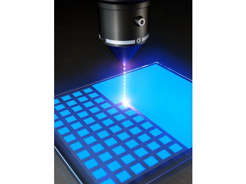 KAIST researchers develops a tech to enable production of ultrahigh-resolution LED with sub-micrometer scale pixels
Ultrahigh-resolution displays are an essential element for developing next-generation electronic products such as virtual reality (VR), augmented reality (AR), and smart watches, and can be applied not only to head-mounted displays, but also to smart glasses and smart lenses. The technology developed through this research is expected to be used to make such next-generation ultrahigh-resolution displays and other various sub-micro optoelectronic devices.
KAIST (President Kwang Hyung Lee) announced on the 22nd that Professor Yong-Hoon Cho's research team of KAIST Department of Physics developed the core technology for an ultrahigh resolution light-emitting diode (LED) display that can realize 0.5 micron-scale pixels smaller than 1/100 of the average hair thickness (about 100 microns) using focused ion beams.
Commonly, pixelation of ultrahigh-resolution LED displays usually relies on the etching method that physically cuts the area around the pixel, but as the pixel becomes smaller due to the occurrence of various defects around it, leading to side-effects of having leakage of current increased and light-emission efficiency decreased. In addition, various complex processes such as patterning for pixelation and post-processing for prevention of leakage current are required.
Professor Yong-Hoon Cho's research team developed a technology that can create pixels down to the size of a microscale without the complicated pre- and post-processing using a focused ion beam. This method has the advantage of being able to freely set the shape of the emitting pixel without causing any structural deformation on the material surface by controlling the intensity of the focused ion beam.
The focused ion beam technology has been widely used for ultrahigh-magnification imaging and nanostructure fabrication in fields such as materials engineering and biology. However, when a focused ion beam is used on a light emitting body such as an LED, light emission of a portion hit by the beam and a surrounding area rapidly decreases, which has been a barrier to fabricating a nano-scale light emitting structure. Upon facing this issue, Professor Cho's research team began the research on the idea that if they turned things around to use these problematic phenomena, they can be used in ultra-fine pixelation method on a sub-micron scale.
The research team used a focused ion beam whose intensity was softened to the extent that the surface was not shaved, and found that not only the light-emission rapidly decreased in the area hit by the focused ion beam, but also the local resistance greatly increased. As a result, while the surface of the LED is kept flat, the portion hit by the focused ion beam is optically and electrically isolated, enabling pixelation for independent operation.
Professor Yong-Hoon Cho, who led the research, said, “We have newly developed a technology that can create sub-micron-scale pixels without complicated processes using a focused ion beam, which will be a base technology that can be applied to next-generation ultrahigh-resolution displays and nano-photoelectronic devices.”
This research in which the Master's student Ji-Hwan Moon and the Ph.D. student Baul Kim of KAIST Department of Physics participated as co-first authors, was carried out with the support of the National Research Foundation of Korea's Support Program for Mid-Career Researchers and the Institute of Information and Communications Technology Planning and Evaluation. It was published online in 'Advanced Materials' on February 13, and was also selected as the internal cover of the next offline edition. (Title: Electrically Driven Sub-Micron Light-Emitting Diode Arrays Using Maskless and Etching-Free Pixelation)
Figure 1. Schematic diagram of the technology for ultrahigh density sub-micron-sized pixels through He focused ion beam (FIB) irradiation on an LED device
Figure 2. Ultra-high-density pixelation technology of micro light-emitting diodes (μLED) through He focused ion beam (FIB) irradiation
Figure 3. Rectangular pixels of different sizes (surface structure picture and luminescence picture) realized by a focused ion beam. Luminescence pictures of pixel arrays ranging in size from 20 µm x 20 µm to 0.5 µm x 0.5 µm, with surface flatness maintained.
2023.03.08 View 9451
KAIST researchers develops a tech to enable production of ultrahigh-resolution LED with sub-micrometer scale pixels
Ultrahigh-resolution displays are an essential element for developing next-generation electronic products such as virtual reality (VR), augmented reality (AR), and smart watches, and can be applied not only to head-mounted displays, but also to smart glasses and smart lenses. The technology developed through this research is expected to be used to make such next-generation ultrahigh-resolution displays and other various sub-micro optoelectronic devices.
KAIST (President Kwang Hyung Lee) announced on the 22nd that Professor Yong-Hoon Cho's research team of KAIST Department of Physics developed the core technology for an ultrahigh resolution light-emitting diode (LED) display that can realize 0.5 micron-scale pixels smaller than 1/100 of the average hair thickness (about 100 microns) using focused ion beams.
Commonly, pixelation of ultrahigh-resolution LED displays usually relies on the etching method that physically cuts the area around the pixel, but as the pixel becomes smaller due to the occurrence of various defects around it, leading to side-effects of having leakage of current increased and light-emission efficiency decreased. In addition, various complex processes such as patterning for pixelation and post-processing for prevention of leakage current are required.
Professor Yong-Hoon Cho's research team developed a technology that can create pixels down to the size of a microscale without the complicated pre- and post-processing using a focused ion beam. This method has the advantage of being able to freely set the shape of the emitting pixel without causing any structural deformation on the material surface by controlling the intensity of the focused ion beam.
The focused ion beam technology has been widely used for ultrahigh-magnification imaging and nanostructure fabrication in fields such as materials engineering and biology. However, when a focused ion beam is used on a light emitting body such as an LED, light emission of a portion hit by the beam and a surrounding area rapidly decreases, which has been a barrier to fabricating a nano-scale light emitting structure. Upon facing this issue, Professor Cho's research team began the research on the idea that if they turned things around to use these problematic phenomena, they can be used in ultra-fine pixelation method on a sub-micron scale.
The research team used a focused ion beam whose intensity was softened to the extent that the surface was not shaved, and found that not only the light-emission rapidly decreased in the area hit by the focused ion beam, but also the local resistance greatly increased. As a result, while the surface of the LED is kept flat, the portion hit by the focused ion beam is optically and electrically isolated, enabling pixelation for independent operation.
Professor Yong-Hoon Cho, who led the research, said, “We have newly developed a technology that can create sub-micron-scale pixels without complicated processes using a focused ion beam, which will be a base technology that can be applied to next-generation ultrahigh-resolution displays and nano-photoelectronic devices.”
This research in which the Master's student Ji-Hwan Moon and the Ph.D. student Baul Kim of KAIST Department of Physics participated as co-first authors, was carried out with the support of the National Research Foundation of Korea's Support Program for Mid-Career Researchers and the Institute of Information and Communications Technology Planning and Evaluation. It was published online in 'Advanced Materials' on February 13, and was also selected as the internal cover of the next offline edition. (Title: Electrically Driven Sub-Micron Light-Emitting Diode Arrays Using Maskless and Etching-Free Pixelation)
Figure 1. Schematic diagram of the technology for ultrahigh density sub-micron-sized pixels through He focused ion beam (FIB) irradiation on an LED device
Figure 2. Ultra-high-density pixelation technology of micro light-emitting diodes (μLED) through He focused ion beam (FIB) irradiation
Figure 3. Rectangular pixels of different sizes (surface structure picture and luminescence picture) realized by a focused ion beam. Luminescence pictures of pixel arrays ranging in size from 20 µm x 20 µm to 0.5 µm x 0.5 µm, with surface flatness maintained.
2023.03.08 View 9451 -
 KAIST Team Develops Surface-Lighting MicroLED Patch with Significant Melanogenesis Inhibition Effect
A KAIST research team led by Ph.d candidate Jae Hee Lee and Professor Keon Jae Lee from the Department of Materials Science and Engineering has developed a surface-lighting microLED patch for UV-induced melanogenesis inhibition.
Melanin is brown or dark pigments existing in the skin, which can be abnormally synthesized by external UV or stress. Since the excessive melanin leads to skin diseases such as spots and freckles, proper treatment is required to return normal skin condition.
Recently, LED-based photo-stimulators have been released for skin care, however, their therapeutic effect is still controversial. Since conventional LED stimulators cannot conformally attach to the human skin, distance-induced side effects are caused by light loss and high heat transfer. To achieve effective phototreatment, the LED stimulator needs to be irradiated in contact with the human skin surface, enabling proper and uniform light deliver to the dermis with minimal optical loss.
In this work, the research team fabricated skin-attachable surface-lighting microLED (SµLED, 4 × 4 cm2) patch by utilizing a thousand of microLED chips and silica-embedded light diffusion layer. 100 µm-sized LED chips are vertically-interconnected for high flexibility and low heat generation, allowing its long-term operation on the human skin.
< Image 1. The overall concept of SµLED patch. a) SµLED patch operated on the human skin. b) Schematic illustration of SµLED patch structure. c) 4 × 4 cm2-sized SµLED patch. d) Schematic illustration of the advantages of SµLED patch such as efficient light delivery, low heat generation, and surface-lighting irradiation. >
The research team confirmed melanogenesis inhibition by irradiating the SµLED patch and the conventional LED (CLED) on the artificial human skin and mice dorsal skin. The SµLED-treated groups of human cells and mouse tissues showed minimal epidermal photo-toxicity and consistently effective reduction in synthesized melanin, compared to CLED-treated groups. In addition, significant suppression of proteins/catalysts expression involved in melanin synthesis such as MITF (microphthalmia-associated transcription factor), Melan-A and tyrosinase was verified.
< Image 2. The efficacy of melanogenesis inhibition on 3D human skin cells. a). Different irradiation conditions for a-MSH (major factor to stimulate melanin synthesis) treated cells. b) The ratio of pigmented area to total epidermis area. c) Relative variance of melanin level in 1 cm2-sized skin cells. A low variance means that melanin is evenly distributed, and a high variance means that the melanin is irregularly distributed. d) Optical images after in vitro experiments for 12 days. Scale bar, 1cm. e) Histological analysis of 3D skin, showing the greatest reduction in melanin after SµLED irradiation. Scale bar, 20 µm. >
< Image 3. The efficacy of melanogenesis inhibition on mouse dorsal skin. a) Optical images of mice dorsal skin after photo-treatment for 20 days. b) Histological analysis of mice dorsal skin. Less brown color means less expression of protein/catalysis involved in melanin synthesis. Scale bar, 50 µm. >
Prof. Keon Jae Lee said, “Our inorganic-based SµLED patch has outstanding characteristics in light efficiency, reliability, and durability. The SµLED patch is expected to give a great impact on the cosmetic field by reducing side effects and maximizing phototherapeutic effects.” The core technology of cosmetic SµLED has been transferred to Fronics co., Ltd, founded by Prof. Lee. Fronics is building foundry and equipment for mass production of SµLED masks for whole face cover and plans to release the products in March next year.
This paper entitled “Wearable Surface-Lighting Micro-Light-Emitting Diode Patch for Melanogenesis Inhibition” was published in the November 2022 issue of Advanced Healthcare Materials.
2022.11.22 View 14199
KAIST Team Develops Surface-Lighting MicroLED Patch with Significant Melanogenesis Inhibition Effect
A KAIST research team led by Ph.d candidate Jae Hee Lee and Professor Keon Jae Lee from the Department of Materials Science and Engineering has developed a surface-lighting microLED patch for UV-induced melanogenesis inhibition.
Melanin is brown or dark pigments existing in the skin, which can be abnormally synthesized by external UV or stress. Since the excessive melanin leads to skin diseases such as spots and freckles, proper treatment is required to return normal skin condition.
Recently, LED-based photo-stimulators have been released for skin care, however, their therapeutic effect is still controversial. Since conventional LED stimulators cannot conformally attach to the human skin, distance-induced side effects are caused by light loss and high heat transfer. To achieve effective phototreatment, the LED stimulator needs to be irradiated in contact with the human skin surface, enabling proper and uniform light deliver to the dermis with minimal optical loss.
In this work, the research team fabricated skin-attachable surface-lighting microLED (SµLED, 4 × 4 cm2) patch by utilizing a thousand of microLED chips and silica-embedded light diffusion layer. 100 µm-sized LED chips are vertically-interconnected for high flexibility and low heat generation, allowing its long-term operation on the human skin.
< Image 1. The overall concept of SµLED patch. a) SµLED patch operated on the human skin. b) Schematic illustration of SµLED patch structure. c) 4 × 4 cm2-sized SµLED patch. d) Schematic illustration of the advantages of SµLED patch such as efficient light delivery, low heat generation, and surface-lighting irradiation. >
The research team confirmed melanogenesis inhibition by irradiating the SµLED patch and the conventional LED (CLED) on the artificial human skin and mice dorsal skin. The SµLED-treated groups of human cells and mouse tissues showed minimal epidermal photo-toxicity and consistently effective reduction in synthesized melanin, compared to CLED-treated groups. In addition, significant suppression of proteins/catalysts expression involved in melanin synthesis such as MITF (microphthalmia-associated transcription factor), Melan-A and tyrosinase was verified.
< Image 2. The efficacy of melanogenesis inhibition on 3D human skin cells. a). Different irradiation conditions for a-MSH (major factor to stimulate melanin synthesis) treated cells. b) The ratio of pigmented area to total epidermis area. c) Relative variance of melanin level in 1 cm2-sized skin cells. A low variance means that melanin is evenly distributed, and a high variance means that the melanin is irregularly distributed. d) Optical images after in vitro experiments for 12 days. Scale bar, 1cm. e) Histological analysis of 3D skin, showing the greatest reduction in melanin after SµLED irradiation. Scale bar, 20 µm. >
< Image 3. The efficacy of melanogenesis inhibition on mouse dorsal skin. a) Optical images of mice dorsal skin after photo-treatment for 20 days. b) Histological analysis of mice dorsal skin. Less brown color means less expression of protein/catalysis involved in melanin synthesis. Scale bar, 50 µm. >
Prof. Keon Jae Lee said, “Our inorganic-based SµLED patch has outstanding characteristics in light efficiency, reliability, and durability. The SµLED patch is expected to give a great impact on the cosmetic field by reducing side effects and maximizing phototherapeutic effects.” The core technology of cosmetic SµLED has been transferred to Fronics co., Ltd, founded by Prof. Lee. Fronics is building foundry and equipment for mass production of SµLED masks for whole face cover and plans to release the products in March next year.
This paper entitled “Wearable Surface-Lighting Micro-Light-Emitting Diode Patch for Melanogenesis Inhibition” was published in the November 2022 issue of Advanced Healthcare Materials.
2022.11.22 View 14199