OT
-
 Wearable Strain Sensor Using Light Transmittance Helps Measure Physical Signals Better
KAIST researchers have developed a novel wearable strain sensor based on the modulation of optical transmittance of a carbon nanotube (CNT)-embedded elastomer. The sensor is capable of sensitive, stable, and continuous measurement of physical signals. This technology, featured in the March 4th issue of ACS Applied Materials & Interfaces as a front cover article, shows great potential for the detection of subtle human motions and the real-time monitoring of body postures for healthcare applications.
A wearable strain sensor must have high sensitivity, flexibility, and stretchability, as well as low cost. Those used especially for health monitoring should also be tied to long-term solid performance, and be environmentally stable. Various stretchable strain sensors based on piezo-resistive and capacitive principles have been developed to meet all these requirements.
Conventional piezo-resistive strain sensors using functional nanomaterials, including CNTs as the most common example, have shown high sensitivity and great sensing performance. However, they suffer from poor long-term stability and linearity, as well as considerable signal hysteresis. As an alternative, piezo-capacitive strain sensors with better stability, lower hysteresis, and higher stretchability have been suggested. But due to the fact that piezo-capacitive strain sensors exhibit limited sensitivity and strong electromagnetic interference caused by the conductive objects in the surrounding environment, these conventional stretchable strain sensors are still facing limitations that are yet to be resolved.
A KAIST research team led by Professor Inkyu Park from the Department of Mechanical Engineering suggested that an optical-type stretchable strain sensor can be a good alternative to resolve the limitations of conventional piezo-resistive and piezo-capacitive strain sensors, because they have high stability and are less affected by environmental disturbances. The team then introduced an optical wearable strain sensor based on the light transmittance changes of a CNT-embedded elastomer, which further addresses the low sensitivity problem of conventional optical stretchable strain sensors.
In order to achieve a large dynamic range for the sensor, Professor Park and his researchers chose Ecoflex as an elastomeric substrate with good mechanical durability, flexibility, and attachability on human skin, and the new optical wearable strain sensor developed by the research group actually shows a wide dynamic range of 0 to 400%.
In addition, the researchers propagated the microcracks under tensile strain within the film of multi-walled CNTs embedded in the Ecoflex substrate, changing the optical transmittance of the film. By doing so, it was possible for them to develop a wearable strain sensor having a sensitivity 10 times higher than conventional optical stretchable strain sensors.
The proposed sensor has also passed the durability test with excellent results. The sensor’s response after 13,000 sets of cyclic loading was stable without any noticeable drift. This suggests that the sensor response can be used without degradation, even if the sensor is repeatedly used for a long time and in various environmental conditions.
Using the developed sensor, the research team could measure the finger bending motion and used it for robot control. They also developed a three-axes sensor array for body posture monitoring. The sensor was able to monitor human motions with small strains such as a pulse near the carotid artery and muscle movement around the mouth during pronunciation.
Professor Park said, “In this study, our group developed a new wearable strain sensor platform that overcomes many limitations of previously developed resistive, capacitive, and optical-type stretchable strain sensors. Our sensor could be widely used in a variety of fields including soft robotics, wearable electronics, electronic skin, healthcare, and even entertainment.”
This work was supported by the National Research Foundation (NRF) of Korea.
Publication:
Jimin Gu, Donguk Kwon, Junseong Ahn, and Inkyu Park. (2020) “Wearable Strain sensors Using Light Transmittance Change of Carbon Nanotube-Embedded Elastomers with Microcracks” ACS Applied Materials & Interfaces. Volume 12. Issue 9. Available online at https://doi.org/10.1021/acsami.9b18069
Profile:
Inkyu Park
Professor
inkyu@kaist.ac.kr
http://mintlab1.kaist.ac.kr
Micro/Nano Transducers Laboratory (MINT Lab)
Department of Mechanical Engineering (ME)Korea Advanced Institute of Science and Technology (KAIST)
Profile:
Jimin Gu
Ph.D. Candidate
mint9411@kaist.ac.kr
http://mintlab1.kaist.ac.kr
MINT Lab
KAIST ME
(END)
2020.03.20 View 12082
Wearable Strain Sensor Using Light Transmittance Helps Measure Physical Signals Better
KAIST researchers have developed a novel wearable strain sensor based on the modulation of optical transmittance of a carbon nanotube (CNT)-embedded elastomer. The sensor is capable of sensitive, stable, and continuous measurement of physical signals. This technology, featured in the March 4th issue of ACS Applied Materials & Interfaces as a front cover article, shows great potential for the detection of subtle human motions and the real-time monitoring of body postures for healthcare applications.
A wearable strain sensor must have high sensitivity, flexibility, and stretchability, as well as low cost. Those used especially for health monitoring should also be tied to long-term solid performance, and be environmentally stable. Various stretchable strain sensors based on piezo-resistive and capacitive principles have been developed to meet all these requirements.
Conventional piezo-resistive strain sensors using functional nanomaterials, including CNTs as the most common example, have shown high sensitivity and great sensing performance. However, they suffer from poor long-term stability and linearity, as well as considerable signal hysteresis. As an alternative, piezo-capacitive strain sensors with better stability, lower hysteresis, and higher stretchability have been suggested. But due to the fact that piezo-capacitive strain sensors exhibit limited sensitivity and strong electromagnetic interference caused by the conductive objects in the surrounding environment, these conventional stretchable strain sensors are still facing limitations that are yet to be resolved.
A KAIST research team led by Professor Inkyu Park from the Department of Mechanical Engineering suggested that an optical-type stretchable strain sensor can be a good alternative to resolve the limitations of conventional piezo-resistive and piezo-capacitive strain sensors, because they have high stability and are less affected by environmental disturbances. The team then introduced an optical wearable strain sensor based on the light transmittance changes of a CNT-embedded elastomer, which further addresses the low sensitivity problem of conventional optical stretchable strain sensors.
In order to achieve a large dynamic range for the sensor, Professor Park and his researchers chose Ecoflex as an elastomeric substrate with good mechanical durability, flexibility, and attachability on human skin, and the new optical wearable strain sensor developed by the research group actually shows a wide dynamic range of 0 to 400%.
In addition, the researchers propagated the microcracks under tensile strain within the film of multi-walled CNTs embedded in the Ecoflex substrate, changing the optical transmittance of the film. By doing so, it was possible for them to develop a wearable strain sensor having a sensitivity 10 times higher than conventional optical stretchable strain sensors.
The proposed sensor has also passed the durability test with excellent results. The sensor’s response after 13,000 sets of cyclic loading was stable without any noticeable drift. This suggests that the sensor response can be used without degradation, even if the sensor is repeatedly used for a long time and in various environmental conditions.
Using the developed sensor, the research team could measure the finger bending motion and used it for robot control. They also developed a three-axes sensor array for body posture monitoring. The sensor was able to monitor human motions with small strains such as a pulse near the carotid artery and muscle movement around the mouth during pronunciation.
Professor Park said, “In this study, our group developed a new wearable strain sensor platform that overcomes many limitations of previously developed resistive, capacitive, and optical-type stretchable strain sensors. Our sensor could be widely used in a variety of fields including soft robotics, wearable electronics, electronic skin, healthcare, and even entertainment.”
This work was supported by the National Research Foundation (NRF) of Korea.
Publication:
Jimin Gu, Donguk Kwon, Junseong Ahn, and Inkyu Park. (2020) “Wearable Strain sensors Using Light Transmittance Change of Carbon Nanotube-Embedded Elastomers with Microcracks” ACS Applied Materials & Interfaces. Volume 12. Issue 9. Available online at https://doi.org/10.1021/acsami.9b18069
Profile:
Inkyu Park
Professor
inkyu@kaist.ac.kr
http://mintlab1.kaist.ac.kr
Micro/Nano Transducers Laboratory (MINT Lab)
Department of Mechanical Engineering (ME)Korea Advanced Institute of Science and Technology (KAIST)
Profile:
Jimin Gu
Ph.D. Candidate
mint9411@kaist.ac.kr
http://mintlab1.kaist.ac.kr
MINT Lab
KAIST ME
(END)
2020.03.20 View 12082 -
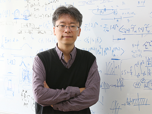
 Scientists Observe the Elusive Kondo Screening Cloud
Scientists ended a 50-year quest by directly observing a quantum phenomenon
An international research group of Professor Heung-Sun Sim has ended a 50-year quest by directly observing a quantum phenomenon known as a Kondo screening cloud. This research, published in Nature on March 11, opens a novel way to engineer spin screening and entanglement. According to the research, the cloud can mediate interactions between distant spins confined in quantum dots, which is a necessary protocol for semiconductor spin-based quantum information processing. This spin-spin interaction mediated by the Kondo cloud is unique since both its strength and sign (two spins favor either parallel or anti-parallel configuration) are electrically tunable, while conventional schemes cannot reverse the sign.
This phenomenon, which is important for many physical phenomena such as dilute magnetic impurities and spin glasses, is essentially a cloud that masks magnetic impurities in a material. It was known to exist but its spatial extension had never been observed, creating controversy over whether such an extension actually existed.
Magnetism arises from a property of electrons known as spin, meaning that they have angular momentum aligned in one of either two directions, conventionally known as up and down. However, due to a phenomenon known as the Kondo effect, the spins of conduction electrons—the electrons that flow freely in a material—become entangled with a localized magnetic impurity, and effectively screen it. The strength of this spin coupling, calibrated as a temperature, is known as the Kondo temperature.
The size of the cloud is another important parameter for a material containing multiple magnetic impurities because the spins in the cloud couple with one another and mediate the coupling between magnetic impurities when the clouds overlap. This happens in various materials such as Kondo lattices, spin glasses, and high temperature superconductors.
Although the Kondo effect for a single magnetic impurity is now a text-book subject in many-body physics, detection of its key object, the Kondo cloud and its length, has remained elusive despite many attempts during the past five decades. Experiments using nuclear magnetic resonance or scanning tunneling microscopy, two common methods for understanding the structure of matter, have either shown no signature of the cloud, or demonstrated a signature only at a very short distance, less than 1 nanometer, so much shorter than the predicted cloud size, which was in the micron range.
In the present study, the authors observed a Kondo screening cloud formed by an impurity defined as a localized electron spin in a quantum dot—a type of “artificial atom”—coupled to quasi-one-dimensional conduction electrons, and then used an interferometer to measure changes in the Kondo temperature, allowing them to investigate the presence of a cloud at the interferometer end.
Essentially, they slightly perturbed the conduction electrons at a location away from the quantum dot using an electrostatic gate. The wave of conducting electrons scattered by this perturbation returned back to the quantum dot and interfered with itself. This is similar to how a wave on a water surface being scattered by a wall forms a stripe pattern. The Kondo cloud is a quantum mechanical object which acts to preserve the wave nature of electrons inside the cloud.
Even though there is no direct electrostatic influence of the perturbation on the quantum dot, this interference modifies the Kondo signature measured by electron conductance through the quantum dot if the perturbation is present inside the cloud. In the study, the researchers found that the length as well as the shape of the cloud is universally scaled by the inverse of the Kondo temperature, and that the cloud’s size and shape were in good agreement with theoretical calculations.
Professor Sim at the Department of Physics proposed the method for detecting the Kondo cloud in the co-research with the RIKEN Center for Emergent Matter Science, the City University of Hong Kong, the University of Tokyo, and Ruhr University Bochum in Germany.
Professor Sim said, “The observed spin cloud is a micrometer-size object that has quantum mechanical wave nature and entanglement. This is why the spin cloud has not been observed despite a long search. It is remarkable in a fundamental and technical point of view that such a large quantum object can now be created, controlled, and detected.
Dr. Michihisa Yamamoto of the RIKEN Center for Emergent Matter Science also said, “It is very satisfying to have been able to obtain real space image of the Kondo cloud, as it is a real breakthrough for understanding various systems containing multiple magnetic impurities. The size of the Kondo cloud in semiconductors was found to be much larger than the typical size of semiconductor devices.”
Publication:
Borzenets et al. (2020) Observation of the Kondo screening cloud. Nature, 579. pp.210-213. Available online at https://doi.org/10.1038/s41586-020-2058-6
Profile:
Heung-Sun Sim, PhD
Professor
hssim@kaist.ac.kr
https://qet.kaist.ac.kr/
Quantum Electron Correlation & Transport Theory Group (QECT Lab)
https://qc.kaist.ac.kr/index.php/group1/
Center for Quantum Coherence In COndensed Matter
Department of Physics
https://www.kaist.ac.kr
Korea Advanced Institute of Science and Technology (KAIST)
Daejeon, Republic of Korea
2020.03.13 View 10347
Scientists Observe the Elusive Kondo Screening Cloud
Scientists ended a 50-year quest by directly observing a quantum phenomenon
An international research group of Professor Heung-Sun Sim has ended a 50-year quest by directly observing a quantum phenomenon known as a Kondo screening cloud. This research, published in Nature on March 11, opens a novel way to engineer spin screening and entanglement. According to the research, the cloud can mediate interactions between distant spins confined in quantum dots, which is a necessary protocol for semiconductor spin-based quantum information processing. This spin-spin interaction mediated by the Kondo cloud is unique since both its strength and sign (two spins favor either parallel or anti-parallel configuration) are electrically tunable, while conventional schemes cannot reverse the sign.
This phenomenon, which is important for many physical phenomena such as dilute magnetic impurities and spin glasses, is essentially a cloud that masks magnetic impurities in a material. It was known to exist but its spatial extension had never been observed, creating controversy over whether such an extension actually existed.
Magnetism arises from a property of electrons known as spin, meaning that they have angular momentum aligned in one of either two directions, conventionally known as up and down. However, due to a phenomenon known as the Kondo effect, the spins of conduction electrons—the electrons that flow freely in a material—become entangled with a localized magnetic impurity, and effectively screen it. The strength of this spin coupling, calibrated as a temperature, is known as the Kondo temperature.
The size of the cloud is another important parameter for a material containing multiple magnetic impurities because the spins in the cloud couple with one another and mediate the coupling between magnetic impurities when the clouds overlap. This happens in various materials such as Kondo lattices, spin glasses, and high temperature superconductors.
Although the Kondo effect for a single magnetic impurity is now a text-book subject in many-body physics, detection of its key object, the Kondo cloud and its length, has remained elusive despite many attempts during the past five decades. Experiments using nuclear magnetic resonance or scanning tunneling microscopy, two common methods for understanding the structure of matter, have either shown no signature of the cloud, or demonstrated a signature only at a very short distance, less than 1 nanometer, so much shorter than the predicted cloud size, which was in the micron range.
In the present study, the authors observed a Kondo screening cloud formed by an impurity defined as a localized electron spin in a quantum dot—a type of “artificial atom”—coupled to quasi-one-dimensional conduction electrons, and then used an interferometer to measure changes in the Kondo temperature, allowing them to investigate the presence of a cloud at the interferometer end.
Essentially, they slightly perturbed the conduction electrons at a location away from the quantum dot using an electrostatic gate. The wave of conducting electrons scattered by this perturbation returned back to the quantum dot and interfered with itself. This is similar to how a wave on a water surface being scattered by a wall forms a stripe pattern. The Kondo cloud is a quantum mechanical object which acts to preserve the wave nature of electrons inside the cloud.
Even though there is no direct electrostatic influence of the perturbation on the quantum dot, this interference modifies the Kondo signature measured by electron conductance through the quantum dot if the perturbation is present inside the cloud. In the study, the researchers found that the length as well as the shape of the cloud is universally scaled by the inverse of the Kondo temperature, and that the cloud’s size and shape were in good agreement with theoretical calculations.
Professor Sim at the Department of Physics proposed the method for detecting the Kondo cloud in the co-research with the RIKEN Center for Emergent Matter Science, the City University of Hong Kong, the University of Tokyo, and Ruhr University Bochum in Germany.
Professor Sim said, “The observed spin cloud is a micrometer-size object that has quantum mechanical wave nature and entanglement. This is why the spin cloud has not been observed despite a long search. It is remarkable in a fundamental and technical point of view that such a large quantum object can now be created, controlled, and detected.
Dr. Michihisa Yamamoto of the RIKEN Center for Emergent Matter Science also said, “It is very satisfying to have been able to obtain real space image of the Kondo cloud, as it is a real breakthrough for understanding various systems containing multiple magnetic impurities. The size of the Kondo cloud in semiconductors was found to be much larger than the typical size of semiconductor devices.”
Publication:
Borzenets et al. (2020) Observation of the Kondo screening cloud. Nature, 579. pp.210-213. Available online at https://doi.org/10.1038/s41586-020-2058-6
Profile:
Heung-Sun Sim, PhD
Professor
hssim@kaist.ac.kr
https://qet.kaist.ac.kr/
Quantum Electron Correlation & Transport Theory Group (QECT Lab)
https://qc.kaist.ac.kr/index.php/group1/
Center for Quantum Coherence In COndensed Matter
Department of Physics
https://www.kaist.ac.kr
Korea Advanced Institute of Science and Technology (KAIST)
Daejeon, Republic of Korea
2020.03.13 View 10347 -
 Professor Hojong Chang’s Research Team Wins ISIITA 2020 Best Paper Award
The paper written by Professor Hojong Chang’s research team from KAIST Institute for IT Convergence won the best paper award from the International Symposium on Innovation in Information Technology Application (ISIITA) 2020, held this month at Ton Duc Thang University in Vietnam.
ISIITA is a networking symposium where leading researchers from various fields including information and communications, biotechnology, and computer systems come together and share on the convergence of technology.
Professor Chang’s team won the best paper award at this year’s symposium with its paper, “A Study of Single Photon Counting System for Quantitative Analysis of Luminescence”. The awarded paper discusses the realization of a signal processing system for silicon photomultipliers.
The silicon photomultiplier is the core of a urinalysis technique that tests for sodium and potassium in the body using simple chemical reactions. If our bodily sodium and potassium levels exceed a certain amount, it can lead to high blood pressure, cardiovascular problems, and kidney damage.
Through this research, the team has developed a core technique that quantifies the sodium and potassium discharged in the urine. When the reagent is injected into the urine, a very small amount of light is emitted as a result of the chemical reaction. However, if there is a large amount of sodium and potassium, they interrupt the reaction and reduce the emission. The key to this measurement technique is digitizing the strength of this very fine emission of light. Professor Chang’s team developed a system that uses a photomultiplier to measure the chemiluminescence.
Professor Chang said, “I look forward for this signal processing system greatly helping to prevent diseases caused by the excessive consumption of sodium and potassium through quick and easy detection.”
Researcher Byunghun Han who carried out the central research for the system design added, “We are planning to focus on miniaturizing the developed technique, so that anyone can carry our device around like a cellphone.”
The research was supported by the Ministry of Science and ICT.
(END)
2020.02.27 View 6349
Professor Hojong Chang’s Research Team Wins ISIITA 2020 Best Paper Award
The paper written by Professor Hojong Chang’s research team from KAIST Institute for IT Convergence won the best paper award from the International Symposium on Innovation in Information Technology Application (ISIITA) 2020, held this month at Ton Duc Thang University in Vietnam.
ISIITA is a networking symposium where leading researchers from various fields including information and communications, biotechnology, and computer systems come together and share on the convergence of technology.
Professor Chang’s team won the best paper award at this year’s symposium with its paper, “A Study of Single Photon Counting System for Quantitative Analysis of Luminescence”. The awarded paper discusses the realization of a signal processing system for silicon photomultipliers.
The silicon photomultiplier is the core of a urinalysis technique that tests for sodium and potassium in the body using simple chemical reactions. If our bodily sodium and potassium levels exceed a certain amount, it can lead to high blood pressure, cardiovascular problems, and kidney damage.
Through this research, the team has developed a core technique that quantifies the sodium and potassium discharged in the urine. When the reagent is injected into the urine, a very small amount of light is emitted as a result of the chemical reaction. However, if there is a large amount of sodium and potassium, they interrupt the reaction and reduce the emission. The key to this measurement technique is digitizing the strength of this very fine emission of light. Professor Chang’s team developed a system that uses a photomultiplier to measure the chemiluminescence.
Professor Chang said, “I look forward for this signal processing system greatly helping to prevent diseases caused by the excessive consumption of sodium and potassium through quick and easy detection.”
Researcher Byunghun Han who carried out the central research for the system design added, “We are planning to focus on miniaturizing the developed technique, so that anyone can carry our device around like a cellphone.”
The research was supported by the Ministry of Science and ICT.
(END)
2020.02.27 View 6349 -
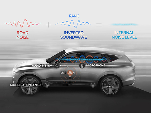 A System Controlling Road Active Noise to Hit the Road
The research team led by Professor Youngjin Park of the Department of Mechanical Engineering has developed a road noise active noise control (RANC) system to be commercialized in partnership with Hyundai Motor Group.
On December 11, Hyundai Motor Group announced the successful development of the RANC system, which significantly reduces the road noise flowing into cars. The carmaker has completed the domestic and American patent applications for the location of sensors and the signal selection method, the core technology of RANC.
RANC is a technology for reducing road noise during driving. This system consists of an acceleration sensor, digital signal processor (the control computer to analyze sound signals), microphone, amplifier, and audio system. To make the system as simple as possible, the audio system utilizes the original audio system embedded in the car instead of a separate system.
The acceleration sensor first calculates the vibration from the road into the car. The location of the sensor is important for accurately identifying the vibration path. The research team was able to find the optimal sensor location through a number of tests.
The System Dynamics and Applied Control Laboratory of Professor Park researched ways to significantly reduce road noise with Hyundai Motor Group for four years from 1993 as a G7 national project and published the results in international journals. In 2002, the researchers published an article titled “Noise Quietens Driving” in Nature, where they announced the first success in reducing road noise in actual cars. The achievement did not lead to commercialization, however, due to the lack of auxiliary technologies at the time, digital amplifiers and DSP for cars for example, and pricing issues.
Since 2013, Professor Park’s research team has participated in one technology transfer and eight university-industry projects. Based on these efforts, the team was able to successfully develop the RANC system with domestic technology in partnership with Hyundai’s NVH Research Lab (Research Fellow, Dr. Gangdeok Lee; Ph.D. in aviation engineering, 1996), Optomech (Founder, Professor Gyeongsu Kim; Ph.D. in mechanical engineering, 1999), ARE (CEO Hyeonseok Kim; Ph.D. in mechanical engineering, 1998), WeAcom, and BurnYoung.
Professor Park’s team led the project by performing theory-based research during the commercialization stage in collaboration with Hyundai Motor Group.
For the commercialization of the RANC system, Hyundai Motor Group is planning to collaborate with the global car audio company Harman to increase the degree of completion and apply the RANC system to the GV 80, the first SUV model of the Genesis brand.
“I am very delighted as an engineer to see the research I worked on from my early days at KAIST be commercialized after 20 years,” noted Professor Park. “I am thrilled to make a contribution to such commercialization with my students in my lab.”
2019.12.27 View 7392
A System Controlling Road Active Noise to Hit the Road
The research team led by Professor Youngjin Park of the Department of Mechanical Engineering has developed a road noise active noise control (RANC) system to be commercialized in partnership with Hyundai Motor Group.
On December 11, Hyundai Motor Group announced the successful development of the RANC system, which significantly reduces the road noise flowing into cars. The carmaker has completed the domestic and American patent applications for the location of sensors and the signal selection method, the core technology of RANC.
RANC is a technology for reducing road noise during driving. This system consists of an acceleration sensor, digital signal processor (the control computer to analyze sound signals), microphone, amplifier, and audio system. To make the system as simple as possible, the audio system utilizes the original audio system embedded in the car instead of a separate system.
The acceleration sensor first calculates the vibration from the road into the car. The location of the sensor is important for accurately identifying the vibration path. The research team was able to find the optimal sensor location through a number of tests.
The System Dynamics and Applied Control Laboratory of Professor Park researched ways to significantly reduce road noise with Hyundai Motor Group for four years from 1993 as a G7 national project and published the results in international journals. In 2002, the researchers published an article titled “Noise Quietens Driving” in Nature, where they announced the first success in reducing road noise in actual cars. The achievement did not lead to commercialization, however, due to the lack of auxiliary technologies at the time, digital amplifiers and DSP for cars for example, and pricing issues.
Since 2013, Professor Park’s research team has participated in one technology transfer and eight university-industry projects. Based on these efforts, the team was able to successfully develop the RANC system with domestic technology in partnership with Hyundai’s NVH Research Lab (Research Fellow, Dr. Gangdeok Lee; Ph.D. in aviation engineering, 1996), Optomech (Founder, Professor Gyeongsu Kim; Ph.D. in mechanical engineering, 1999), ARE (CEO Hyeonseok Kim; Ph.D. in mechanical engineering, 1998), WeAcom, and BurnYoung.
Professor Park’s team led the project by performing theory-based research during the commercialization stage in collaboration with Hyundai Motor Group.
For the commercialization of the RANC system, Hyundai Motor Group is planning to collaborate with the global car audio company Harman to increase the degree of completion and apply the RANC system to the GV 80, the first SUV model of the Genesis brand.
“I am very delighted as an engineer to see the research I worked on from my early days at KAIST be commercialized after 20 years,” noted Professor Park. “I am thrilled to make a contribution to such commercialization with my students in my lab.”
2019.12.27 View 7392 -
 Two Professors Receive Awards from the Korea Robotics Society
< Professor Jee-Hwan Ryu and Professor Ayoung Kim >
The Korea Robotics Society (KROS) conferred awards onto two KAIST professors from the Department of Civil and Environmental Engineering in recognition of their achievements and contributions to the development of the robotics industry in 2019. Professor Jee-Hwan Ryu has been actively engaged in researching the field of teleoperation, and this led him to win the KROS Robotics Innovation (KRI) Award. The KRI Award was newly established in 2019 by the KROS, in order to encourage researchers who have made innovative achievements in robotics. Professor Ryu shared the honor of being the first winner of this award with Professor Jaeheung Park of Seoul National University. Professor Ayoung Kim, from the same department, received the Young Investigator Award presented to emerging robitics researchers under 40 years of age. (END)
2019.12.19 View 6044
Two Professors Receive Awards from the Korea Robotics Society
< Professor Jee-Hwan Ryu and Professor Ayoung Kim >
The Korea Robotics Society (KROS) conferred awards onto two KAIST professors from the Department of Civil and Environmental Engineering in recognition of their achievements and contributions to the development of the robotics industry in 2019. Professor Jee-Hwan Ryu has been actively engaged in researching the field of teleoperation, and this led him to win the KROS Robotics Innovation (KRI) Award. The KRI Award was newly established in 2019 by the KROS, in order to encourage researchers who have made innovative achievements in robotics. Professor Ryu shared the honor of being the first winner of this award with Professor Jaeheung Park of Seoul National University. Professor Ayoung Kim, from the same department, received the Young Investigator Award presented to emerging robitics researchers under 40 years of age. (END)
2019.12.19 View 6044 -
 ‘Carrier-Resolved Photo-Hall’ to Push Semiconductor Advances
(Professor Shin and Dr. Gunawan (left))
An IBM-KAIST research team described a breakthrough in a 140-year-old mystery in physics. The research reported in Nature last month unlocks the physical characteristics of semiconductors in much greater detail and aids in the development of new and improved semiconductor materials.
Research team under Professor Byungha Shin at the Department of Material Sciences and Engineering and Dr. Oki Gunawan at IBM discovered a new formula and technique that enables the simultaneous extraction of both majority and minority carrier information such as their density and mobility, as well as gain additional insights about carrier lifetimes, diffusion lengths, and the recombination process. This new discovery and technology will help push semiconductor advances in both existing and emerging technologies.
Semiconductors are the basic building blocks of today’s digital electronics age, providing us with a multitude of devices that benefit our modern life. To truly appreciate the physics of semiconductors, it is very important to understand the fundamental properties of the charge carriers inside the materials, whether those particles are positive or negative, their speed under an applied electric field, and how densely they are packed into the material.
Physicist Edwin Hall found a way to determine those properties in 1879, when he discovered that a magnetic field will deflect the movement of electronic charges inside a conductor and that the amount of deflection can be measured as a voltage perpendicular to the flow of the charge. Decades after Hall’s discovery, researchers also recognized that they can measure the Hall effect with light via “photo-Hall experiments”. During such experiments, the light generates multiple carriers or electron–hole pairs in the semiconductors.
Unfortunately, the basic Hall effect only provided insights into the dominant charge carrier (or majority carrier). Researchers were unable to extract the properties of both carriers (the majority and minority carriers) simultaneously. The property information of both carriers is crucial for many applications that involve light such as solar cells and other optoelectronic devices.
In the photo-Hall experiment by the KAIST-IBM team, both carriers contribute to changes in conductivity and the Hall coefficient. The key insight comes from measuring the conductivity and Hall coefficient as a function of light intensity. Hidden in the trajectory of the conductivity, the Hall coefficient curve reveals crucial new information: the difference in the mobility of both carriers. As discussed in the paper, this relationship can be expressed elegantly as: Δµ = d (σ²H)/dσ
The research team solved for both majority and minority carrier mobility and density as a function of light intensity, naming the new technique Carrier-Resolved Photo Hall (CRPH) measurement. With known light illumination intensity, the carrier lifetime can be established in a similar way.
Beyond advances in theoretical understanding, advances in experimental techniques were also critical for enabling this breakthrough. The technique requires a clean Hall signal measurement, which can be challenging for materials where the Hall signal is weak due to low mobility or when extra unwanted signals are present, such as under strong light illumination.
The newly developed photo-Hall technique allows the extraction of an astonishing amount of information from semiconductors. In contrast to only three parameters obtained in the classic Hall measurements, this new technique yields up to seven parameters at every tested level of light intensity. These include the mobility of both the electron and hole; their carrier density under light; the recombination lifetime; and the diffusion lengths for electrons, holes, and ambipolar types. All of these can be repeated N times (i.e. the number of light intensity settings used in the experiment).
Professor Shin said, “This novel technology sheds new light on understanding the physical characteristics of semiconductor materials in great detail.” Dr. Gunawan added, “This will will help accelerate the development of next-generation semiconductor technology such as better solar cells, better optoelectronics devices, and new materials and devices for artificial intelligence technology.”
Profile:
Professor Byungha Shin
Department of Materials Science and Engineering
KAIST
byungha@kaist.ac.kr
http://energymatlab.kaist.ac.kr/
2019.11.18 View 10328
‘Carrier-Resolved Photo-Hall’ to Push Semiconductor Advances
(Professor Shin and Dr. Gunawan (left))
An IBM-KAIST research team described a breakthrough in a 140-year-old mystery in physics. The research reported in Nature last month unlocks the physical characteristics of semiconductors in much greater detail and aids in the development of new and improved semiconductor materials.
Research team under Professor Byungha Shin at the Department of Material Sciences and Engineering and Dr. Oki Gunawan at IBM discovered a new formula and technique that enables the simultaneous extraction of both majority and minority carrier information such as their density and mobility, as well as gain additional insights about carrier lifetimes, diffusion lengths, and the recombination process. This new discovery and technology will help push semiconductor advances in both existing and emerging technologies.
Semiconductors are the basic building blocks of today’s digital electronics age, providing us with a multitude of devices that benefit our modern life. To truly appreciate the physics of semiconductors, it is very important to understand the fundamental properties of the charge carriers inside the materials, whether those particles are positive or negative, their speed under an applied electric field, and how densely they are packed into the material.
Physicist Edwin Hall found a way to determine those properties in 1879, when he discovered that a magnetic field will deflect the movement of electronic charges inside a conductor and that the amount of deflection can be measured as a voltage perpendicular to the flow of the charge. Decades after Hall’s discovery, researchers also recognized that they can measure the Hall effect with light via “photo-Hall experiments”. During such experiments, the light generates multiple carriers or electron–hole pairs in the semiconductors.
Unfortunately, the basic Hall effect only provided insights into the dominant charge carrier (or majority carrier). Researchers were unable to extract the properties of both carriers (the majority and minority carriers) simultaneously. The property information of both carriers is crucial for many applications that involve light such as solar cells and other optoelectronic devices.
In the photo-Hall experiment by the KAIST-IBM team, both carriers contribute to changes in conductivity and the Hall coefficient. The key insight comes from measuring the conductivity and Hall coefficient as a function of light intensity. Hidden in the trajectory of the conductivity, the Hall coefficient curve reveals crucial new information: the difference in the mobility of both carriers. As discussed in the paper, this relationship can be expressed elegantly as: Δµ = d (σ²H)/dσ
The research team solved for both majority and minority carrier mobility and density as a function of light intensity, naming the new technique Carrier-Resolved Photo Hall (CRPH) measurement. With known light illumination intensity, the carrier lifetime can be established in a similar way.
Beyond advances in theoretical understanding, advances in experimental techniques were also critical for enabling this breakthrough. The technique requires a clean Hall signal measurement, which can be challenging for materials where the Hall signal is weak due to low mobility or when extra unwanted signals are present, such as under strong light illumination.
The newly developed photo-Hall technique allows the extraction of an astonishing amount of information from semiconductors. In contrast to only three parameters obtained in the classic Hall measurements, this new technique yields up to seven parameters at every tested level of light intensity. These include the mobility of both the electron and hole; their carrier density under light; the recombination lifetime; and the diffusion lengths for electrons, holes, and ambipolar types. All of these can be repeated N times (i.e. the number of light intensity settings used in the experiment).
Professor Shin said, “This novel technology sheds new light on understanding the physical characteristics of semiconductor materials in great detail.” Dr. Gunawan added, “This will will help accelerate the development of next-generation semiconductor technology such as better solar cells, better optoelectronics devices, and new materials and devices for artificial intelligence technology.”
Profile:
Professor Byungha Shin
Department of Materials Science and Engineering
KAIST
byungha@kaist.ac.kr
http://energymatlab.kaist.ac.kr/
2019.11.18 View 10328 -
 Ultrafast Quantum Motion in a Nanoscale Trap Detected
< Professor Heung-Sun Sim (left) and Co-author Dr. Sungguen Ryu (right) >
KAIST researchers have reported the detection of a picosecond electron motion in a silicon transistor. This study has presented a new protocol for measuring ultrafast electronic dynamics in an effective time-resolved fashion of picosecond resolution. The detection was made in collaboration with Nippon Telegraph and Telephone Corp. (NTT) in Japan and National Physical Laboratory (NPL) in the UK and is the first report to the best of our knowledge.
When an electron is captured in a nanoscale trap in solids, its quantum mechanical wave function can exhibit spatial oscillation at sub-terahertz frequencies. Time-resolved detection of such picosecond dynamics of quantum waves is important, as the detection provides a way of understanding the quantum behavior of electrons in nano-electronics. It also applies to quantum information technologies such as the ultrafast quantum-bit operation of quantum computing and high-sensitivity electromagnetic-field sensing. However, detecting picosecond dynamics has been a challenge since the sub-terahertz scale is far beyond the latest bandwidth measurement tools.
A KAIST team led by Professor Heung-Sun Sim developed a theory of ultrafast electron dynamics in a nanoscale trap, and proposed a scheme for detecting the dynamics, which utilizes a quantum-mechanical resonant state formed beside the trap. The coupling between the electron dynamics and the resonant state is switched on and off at a picosecond so that information on the dynamics is read out on the electric current being generated when the coupling is switched on.
NTT realized, together with NPL, the detection scheme and applied it to electron motions in a nanoscale trap formed in a silicon transistor. A single electron was captured in the trap by controlling electrostatic gates, and a resonant state was formed in the potential barrier of the trap.
The switching on and off of the coupling between the electron and the resonant state was achieved by aligning the resonance energy with the energy of the electron within a picosecond. An electric current from the trap through the resonant state to an electrode was measured at only a few Kelvin degrees, unveiling the spatial quantum-coherent oscillation of the electron with 250 GHz frequency inside the trap.
Professor Sim said, “This work suggests a scheme of detecting picosecond electron motions in submicron scales by utilizing quantum resonance. It will be useful in dynamical control of quantum mechanical electron waves for various purposes in nano-electronics, quantum sensing, and quantum information”.
This work was published online at Nature Nanotechnology on November 4. It was partly supported by the Korea National Research Foundation through the SRC Center for Quantum Coherence in Condensed Matter. For more on the NTT news release this article, please visit https://www.ntt.co.jp/news2019/1911e/191105a.html
-ProfileProfessor Heung-Sun Sim
Department of PhysicsDirector, SRC Center for Quantum Coherence in Condensed Matterhttps://qet.kaist.ac.kr KAIST
-Publication:Gento Yamahata, Sungguen Ryu, Nathan Johnson, H.-S. Sim, Akira Fujiwara, and Masaya Kataoka. 2019. Picosecond coherent electron motion in a silicon single-electron source. Nature Nanotechnology (Online Publication). 6 pages. https://doi.org/10.1038/s41565-019-0563-2
2019.11.05 View 13122
Ultrafast Quantum Motion in a Nanoscale Trap Detected
< Professor Heung-Sun Sim (left) and Co-author Dr. Sungguen Ryu (right) >
KAIST researchers have reported the detection of a picosecond electron motion in a silicon transistor. This study has presented a new protocol for measuring ultrafast electronic dynamics in an effective time-resolved fashion of picosecond resolution. The detection was made in collaboration with Nippon Telegraph and Telephone Corp. (NTT) in Japan and National Physical Laboratory (NPL) in the UK and is the first report to the best of our knowledge.
When an electron is captured in a nanoscale trap in solids, its quantum mechanical wave function can exhibit spatial oscillation at sub-terahertz frequencies. Time-resolved detection of such picosecond dynamics of quantum waves is important, as the detection provides a way of understanding the quantum behavior of electrons in nano-electronics. It also applies to quantum information technologies such as the ultrafast quantum-bit operation of quantum computing and high-sensitivity electromagnetic-field sensing. However, detecting picosecond dynamics has been a challenge since the sub-terahertz scale is far beyond the latest bandwidth measurement tools.
A KAIST team led by Professor Heung-Sun Sim developed a theory of ultrafast electron dynamics in a nanoscale trap, and proposed a scheme for detecting the dynamics, which utilizes a quantum-mechanical resonant state formed beside the trap. The coupling between the electron dynamics and the resonant state is switched on and off at a picosecond so that information on the dynamics is read out on the electric current being generated when the coupling is switched on.
NTT realized, together with NPL, the detection scheme and applied it to electron motions in a nanoscale trap formed in a silicon transistor. A single electron was captured in the trap by controlling electrostatic gates, and a resonant state was formed in the potential barrier of the trap.
The switching on and off of the coupling between the electron and the resonant state was achieved by aligning the resonance energy with the energy of the electron within a picosecond. An electric current from the trap through the resonant state to an electrode was measured at only a few Kelvin degrees, unveiling the spatial quantum-coherent oscillation of the electron with 250 GHz frequency inside the trap.
Professor Sim said, “This work suggests a scheme of detecting picosecond electron motions in submicron scales by utilizing quantum resonance. It will be useful in dynamical control of quantum mechanical electron waves for various purposes in nano-electronics, quantum sensing, and quantum information”.
This work was published online at Nature Nanotechnology on November 4. It was partly supported by the Korea National Research Foundation through the SRC Center for Quantum Coherence in Condensed Matter. For more on the NTT news release this article, please visit https://www.ntt.co.jp/news2019/1911e/191105a.html
-ProfileProfessor Heung-Sun Sim
Department of PhysicsDirector, SRC Center for Quantum Coherence in Condensed Matterhttps://qet.kaist.ac.kr KAIST
-Publication:Gento Yamahata, Sungguen Ryu, Nathan Johnson, H.-S. Sim, Akira Fujiwara, and Masaya Kataoka. 2019. Picosecond coherent electron motion in a silicon single-electron source. Nature Nanotechnology (Online Publication). 6 pages. https://doi.org/10.1038/s41565-019-0563-2
2019.11.05 View 13122 -
 Professor Byong-Guk Park Named Scientist of October
< Professor Byong-Guk Park >
Professor Byong-Guk Park from the Department of Materials Science and Engineering was selected as the ‘Scientist of the Month’ for October 2019 by the Ministry of Science and ICT and the National Research Foundation of Korea. Professor Park was recognized for his contributions to the advancement of spin-orbit torque (SOT)-based magnetic random access memory (MRAM) technology. He received 10 million KRW in prize money.
A next-generation, non-volatile memory device MRAM consists of thin magnetic films. It can be applied in “logic-in-memory” devices, in which logic and memory functionalities coexist, thus drastically improving the performance of complementary metal-oxide semiconductor (CMOS) processors. Conventional MRAM technology is limited in its ability to increase the operation speed of a memory device while maintaining a high density.
Professor Park tackled this challenge by introducing a new material, antiferromagnet (IrMn), that generates a sizable amount of SOT as well as an exchange-bias field, which makes successful data writing possible without an external magnetic field. This research outcome paved the way for the development of MRAM, which has a simple device structure but features high speeds and density.
Professor Park said, “I feel rewarded to have forwarded the feasibility and applicability of MRAM. I will continue devoting myself to studying further on the development of new materials that can help enhance the performance of memory devices."
(END)
2019.10.10 View 6094
Professor Byong-Guk Park Named Scientist of October
< Professor Byong-Guk Park >
Professor Byong-Guk Park from the Department of Materials Science and Engineering was selected as the ‘Scientist of the Month’ for October 2019 by the Ministry of Science and ICT and the National Research Foundation of Korea. Professor Park was recognized for his contributions to the advancement of spin-orbit torque (SOT)-based magnetic random access memory (MRAM) technology. He received 10 million KRW in prize money.
A next-generation, non-volatile memory device MRAM consists of thin magnetic films. It can be applied in “logic-in-memory” devices, in which logic and memory functionalities coexist, thus drastically improving the performance of complementary metal-oxide semiconductor (CMOS) processors. Conventional MRAM technology is limited in its ability to increase the operation speed of a memory device while maintaining a high density.
Professor Park tackled this challenge by introducing a new material, antiferromagnet (IrMn), that generates a sizable amount of SOT as well as an exchange-bias field, which makes successful data writing possible without an external magnetic field. This research outcome paved the way for the development of MRAM, which has a simple device structure but features high speeds and density.
Professor Park said, “I feel rewarded to have forwarded the feasibility and applicability of MRAM. I will continue devoting myself to studying further on the development of new materials that can help enhance the performance of memory devices."
(END)
2019.10.10 View 6094 -
 Object Identification and Interaction with a Smartphone Knock
(Professor Lee (far right) demonstrate 'Knocker' with his students.)
A KAIST team has featured a new technology, “Knocker”, which identifies objects and executes actions just by knocking on it with the smartphone. Software powered by machine learning of sounds, vibrations, and other reactions will perform the users’ directions.
What separates Knocker from existing technology is the sensor fusion of sound and motion. Previously, object identification used either computer vision technology with cameras or hardware such as RFID (Radio Frequency Identification) tags. These solutions all have their limitations. For computer vision technology, users need to take pictures of every item. Even worse, the technology will not work well in poor lighting situations. Using hardware leads to additional costs and labor burdens.
Knocker, on the other hand, can identify objects even in dark environments only with a smartphone, without requiring any specialized hardware or using a camera. Knocker utilizes the smartphone’s built-in sensors such as a microphone, an accelerometer, and a gyroscope to capture a unique set of responses generated when a smartphone is knocked against an object. Machine learning is used to analyze these responses and classify and identify objects.
The research team under Professor Sung-Ju Lee from the School of Computing confirmed the applicability of Knocker technology using 23 everyday objects such as books, laptop computers, water bottles, and bicycles. In noisy environments such as a busy café or on the side of a road, it achieved 83% identification accuracy. In a quiet indoor environment, the accuracy rose to 98%.
The team believes Knocker will open a new paradigm of object interaction. For instance, by knocking on an empty water bottle, a smartphone can automatically order new water bottles from a merchant app. When integrated with IoT devices, knocking on a bed’s headboard before going to sleep could turn off the lights and set an alarm. The team suggested and implemented 15 application cases in the paper, presented during the 2019 ACM International Joint Conference on Pervasive and Ubiquitous Computing (UbiComp 2019) held in London last month.
Professor Sung-Ju Lee said, “This new technology does not require any specialized sensor or hardware. It simply uses the built-in sensors on smartphones and takes advantage of the power of machine learning. It’s a software solution that everyday smartphone users could immediately benefit from.” He continued, “This technology enables users to conveniently interact with their favorite objects.”
The research was supported in part by the Next-Generation Information Computing Development Program through the National Research Foundation of Korea funded by the Ministry of Science and ICT and an Institute for Information & Communications Technology Promotion (IITP) grant funded by the Ministry of Science and ICT.
Figure: An example knock on a bottle. Knocker identifies the object by analyzing a unique set of responses from the knock, and automatically launches a proper application or service.
2019.10.02 View 22368
Object Identification and Interaction with a Smartphone Knock
(Professor Lee (far right) demonstrate 'Knocker' with his students.)
A KAIST team has featured a new technology, “Knocker”, which identifies objects and executes actions just by knocking on it with the smartphone. Software powered by machine learning of sounds, vibrations, and other reactions will perform the users’ directions.
What separates Knocker from existing technology is the sensor fusion of sound and motion. Previously, object identification used either computer vision technology with cameras or hardware such as RFID (Radio Frequency Identification) tags. These solutions all have their limitations. For computer vision technology, users need to take pictures of every item. Even worse, the technology will not work well in poor lighting situations. Using hardware leads to additional costs and labor burdens.
Knocker, on the other hand, can identify objects even in dark environments only with a smartphone, without requiring any specialized hardware or using a camera. Knocker utilizes the smartphone’s built-in sensors such as a microphone, an accelerometer, and a gyroscope to capture a unique set of responses generated when a smartphone is knocked against an object. Machine learning is used to analyze these responses and classify and identify objects.
The research team under Professor Sung-Ju Lee from the School of Computing confirmed the applicability of Knocker technology using 23 everyday objects such as books, laptop computers, water bottles, and bicycles. In noisy environments such as a busy café or on the side of a road, it achieved 83% identification accuracy. In a quiet indoor environment, the accuracy rose to 98%.
The team believes Knocker will open a new paradigm of object interaction. For instance, by knocking on an empty water bottle, a smartphone can automatically order new water bottles from a merchant app. When integrated with IoT devices, knocking on a bed’s headboard before going to sleep could turn off the lights and set an alarm. The team suggested and implemented 15 application cases in the paper, presented during the 2019 ACM International Joint Conference on Pervasive and Ubiquitous Computing (UbiComp 2019) held in London last month.
Professor Sung-Ju Lee said, “This new technology does not require any specialized sensor or hardware. It simply uses the built-in sensors on smartphones and takes advantage of the power of machine learning. It’s a software solution that everyday smartphone users could immediately benefit from.” He continued, “This technology enables users to conveniently interact with their favorite objects.”
The research was supported in part by the Next-Generation Information Computing Development Program through the National Research Foundation of Korea funded by the Ministry of Science and ICT and an Institute for Information & Communications Technology Promotion (IITP) grant funded by the Ministry of Science and ICT.
Figure: An example knock on a bottle. Knocker identifies the object by analyzing a unique set of responses from the knock, and automatically launches a proper application or service.
2019.10.02 View 22368 -
 Chair Professor Jo-Won Lee Named Sixth President of National Nano Fab Center
< President Jo-Won Lee >
Chair professor Jo-Won Lee from Hanyang University was appointed as the sixth president of the National Nano Fab Center (NNFC). President Lee will serve his term for three years from September 16.
The NNFC is an affiliated institution of KAIST, established in 2002 to foster qualified manpower in the field of nanotechnology (NT) in Korea. The NNFC features cutting-edge NT-related research equipment and fabrication services, and provides students and researchers quality education and training. The NNFC seeks to become a world-leading institute by performing extensive business operations including the commercialization of NT research results and conducting various multidisciplinary projects.
President Lee received his BS degree from Hanyang University and his MS and PhD degrees in metals science from the Pennsylvania State University. He taught nano-conversion science at his alma mater, Hanyang University, while serving as the director of the National Program for Tera-level Nanodevices. President Lee also guided the governmental planning committee for the 10-year Korea Nanotechnology Initiative as secretary general.
President Lee said, “The NNFC has been striving to develop Korea as the world’s strongest nation in nanotechnology thus far. All of the members of the NNFC will continue giving our best effort for the improvement of our nation’s nanotechnology.”
(END)
2019.09.17 View 2439
Chair Professor Jo-Won Lee Named Sixth President of National Nano Fab Center
< President Jo-Won Lee >
Chair professor Jo-Won Lee from Hanyang University was appointed as the sixth president of the National Nano Fab Center (NNFC). President Lee will serve his term for three years from September 16.
The NNFC is an affiliated institution of KAIST, established in 2002 to foster qualified manpower in the field of nanotechnology (NT) in Korea. The NNFC features cutting-edge NT-related research equipment and fabrication services, and provides students and researchers quality education and training. The NNFC seeks to become a world-leading institute by performing extensive business operations including the commercialization of NT research results and conducting various multidisciplinary projects.
President Lee received his BS degree from Hanyang University and his MS and PhD degrees in metals science from the Pennsylvania State University. He taught nano-conversion science at his alma mater, Hanyang University, while serving as the director of the National Program for Tera-level Nanodevices. President Lee also guided the governmental planning committee for the 10-year Korea Nanotechnology Initiative as secretary general.
President Lee said, “The NNFC has been striving to develop Korea as the world’s strongest nation in nanotechnology thus far. All of the members of the NNFC will continue giving our best effort for the improvement of our nation’s nanotechnology.”
(END)
2019.09.17 View 2439 -
 Sungjoon Park Named Google PhD Fellow
PhD candidate Sungjoon Park from the School of Computing was named a 2019 Google PhD Fellow in the field of natural language processing. The Google PhD fellowship program has recognized and supported outstanding graduate students in computer science and related fields since 2009. Park is one of three Korean students chosen as the recipients of Google Fellowships this year. A total of 54 students across the world in 12 fields were awarded this fellowship.
Park’s research on computational psychotherapy using natural language processing (NLP) powered by machine learning earned him this year’s fellowship. He presented of learning distributed representations in Korean and their interpretations during the 2017 Annual Conference of the Association for Computational Linguistics and the 2018 Conference on Empirical Methods in Natural Language Processing. He also applied machine learning-based natural language processing into computational psychotherapy so that a trained machine learning model could categorize client's verbal responses in a counseling dialogue. This was presented at the Annual Conference of the North American Chapter of the Association for Computational Linguistics.
More recently, he has been developing on neural response generation model and the prediction and extraction of complex emotion in text, and computational psychotherapy applications.
2019.09.17 View 5205
Sungjoon Park Named Google PhD Fellow
PhD candidate Sungjoon Park from the School of Computing was named a 2019 Google PhD Fellow in the field of natural language processing. The Google PhD fellowship program has recognized and supported outstanding graduate students in computer science and related fields since 2009. Park is one of three Korean students chosen as the recipients of Google Fellowships this year. A total of 54 students across the world in 12 fields were awarded this fellowship.
Park’s research on computational psychotherapy using natural language processing (NLP) powered by machine learning earned him this year’s fellowship. He presented of learning distributed representations in Korean and their interpretations during the 2017 Annual Conference of the Association for Computational Linguistics and the 2018 Conference on Empirical Methods in Natural Language Processing. He also applied machine learning-based natural language processing into computational psychotherapy so that a trained machine learning model could categorize client's verbal responses in a counseling dialogue. This was presented at the Annual Conference of the North American Chapter of the Association for Computational Linguistics.
More recently, he has been developing on neural response generation model and the prediction and extraction of complex emotion in text, and computational psychotherapy applications.
2019.09.17 View 5205 -
 Two More Cross-generation Collaborative Labs Open
< President Sung-Chul Shin (sixth from the left) and Professor Sun Chang Kim (seventh from the left) at the signboard ceremony of KAIST BioDesigneering Laboratory >
KAIST opened two more cross-generation collaborative labs last month. KAIST BioDesigneering Laboratory headed by Professor Sun Chang Kim from the Department of Biological Sciences and Nanophotonics Laboratory led by Professor Yong-Hee Lee from the Department of Physics have been selected to receive 500 million KRW funding for five years.
A four-member selection committee including the former President of ETH Zürich Professor Emeritus Ralph Eichler and Professor Kwang-Soo Kim of Harvard Medical School conducted a three-month review and evaluation for this selection to be made. With these two new labs onboard, a total of six cross-generation collaborative labs will be operated on campus.
The operation of cross-generation collaborative labs has been in trial since March last year, as one of the KAIST’s Vision 2031 research innovation initiatives. This novel approach is to pair up senior and junior faculty members for sustaining research and academic achievements even after the senior researcher retires, so that the spectrum of knowledge and research competitiveness can be extended to future generations. The selected labs will be funded for five years, and the funding will be extended if necessary. KAIST will continue to select new labs every year.
One of this year’s selectees Professor Sun Chang Kim will be teamed up with Professor Byung-Kwan Cho from the same department and Professor Jung Kyoon Choi from the Department of Bio and Brain Engineering to collaborate in the fields of synthetic biology, systems biology, and genetic engineering. This group mainly aims at designing and synthesizing optimal genomes that can efficiently manufacture protein drug and biomedical active materials. They will also strive to secure large amounts of high-functioning natural active substances, new adhesive antibacterial peptides, and eco-friendly ecological restoration materials. It is expected that collaboration between these three multigenerational professors will help innovate their bio-convergence technology and further strengthen their international competitiveness in the global bio-market.
Another world-renowned scholar Professor Yong-Hee Lee of photonic crystal laser study will be joined by Professor Minkyo Seo from the same department and Professor Hansuek Lee from the Graduate School of Nanoscience and Technology. They will explore the extreme limits of light-material interaction based on optical micro/nano resonators, with the goal of developing future nonlinear optoelectronic and quantum optical devices. The knowledge and technology newly gained from the research are expected to provide an important platform for a diverse range of fields from quantum communications to biophysics.
(END)
2019.09.06 View 6586
Two More Cross-generation Collaborative Labs Open
< President Sung-Chul Shin (sixth from the left) and Professor Sun Chang Kim (seventh from the left) at the signboard ceremony of KAIST BioDesigneering Laboratory >
KAIST opened two more cross-generation collaborative labs last month. KAIST BioDesigneering Laboratory headed by Professor Sun Chang Kim from the Department of Biological Sciences and Nanophotonics Laboratory led by Professor Yong-Hee Lee from the Department of Physics have been selected to receive 500 million KRW funding for five years.
A four-member selection committee including the former President of ETH Zürich Professor Emeritus Ralph Eichler and Professor Kwang-Soo Kim of Harvard Medical School conducted a three-month review and evaluation for this selection to be made. With these two new labs onboard, a total of six cross-generation collaborative labs will be operated on campus.
The operation of cross-generation collaborative labs has been in trial since March last year, as one of the KAIST’s Vision 2031 research innovation initiatives. This novel approach is to pair up senior and junior faculty members for sustaining research and academic achievements even after the senior researcher retires, so that the spectrum of knowledge and research competitiveness can be extended to future generations. The selected labs will be funded for five years, and the funding will be extended if necessary. KAIST will continue to select new labs every year.
One of this year’s selectees Professor Sun Chang Kim will be teamed up with Professor Byung-Kwan Cho from the same department and Professor Jung Kyoon Choi from the Department of Bio and Brain Engineering to collaborate in the fields of synthetic biology, systems biology, and genetic engineering. This group mainly aims at designing and synthesizing optimal genomes that can efficiently manufacture protein drug and biomedical active materials. They will also strive to secure large amounts of high-functioning natural active substances, new adhesive antibacterial peptides, and eco-friendly ecological restoration materials. It is expected that collaboration between these three multigenerational professors will help innovate their bio-convergence technology and further strengthen their international competitiveness in the global bio-market.
Another world-renowned scholar Professor Yong-Hee Lee of photonic crystal laser study will be joined by Professor Minkyo Seo from the same department and Professor Hansuek Lee from the Graduate School of Nanoscience and Technology. They will explore the extreme limits of light-material interaction based on optical micro/nano resonators, with the goal of developing future nonlinear optoelectronic and quantum optical devices. The knowledge and technology newly gained from the research are expected to provide an important platform for a diverse range of fields from quantum communications to biophysics.
(END)
2019.09.06 View 6586