LED
-
 KAIST Research Team Develops Electronic Ink for Room-Temperature Printing of High-Resolution, Variable-Stiffness Electronics
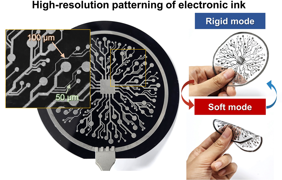
A team of researchers from KAIST and Seoul National University has developed a groundbreaking electronic ink that enables room-temperature printing of variable-stiffness circuits capable of switching between rigid and soft modes. This advancement marks a significant leap toward next-generation wearable, implantable, and robotic devices.
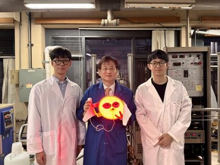
< Photo 1. (From left) Professor Jae-Woong Jeong and PhD candidate Simok Lee of the School of Electrical Engineering, (in separate bubbles, from left) Professor Gun-Hee Lee of Pusan National University, Professor Seongjun Park of Seoul National University, Professor Steve Park of the Department of Materials Science and Engineering>
Variable-stiffness electronics are at the forefront of adaptive technology, offering the ability for a single device to transition between rigid and soft modes depending on its use case. Gallium, a metal known for its high rigidity contrast between solid and liquid states, is a promising candidate for such applications. However, its use has been hindered by challenges including high surface tension, low viscosity, and undesirable phase transitions during manufacturing.
On June 4th, a research team led by Professor Jae-Woong Jeong from the School of Electrical Engineering at KAIST, Professor Seongjun Park from the Digital Healthcare Major at Seoul National University, and Professor Steve Park from the Department of Materials Science and Engineering at KAIST introduced a novel liquid metal electronic ink. This ink allows for micro-scale circuit printing – thinner than a human hair – at room temperature, with the ability to reversibly switch between rigid and soft modes depending on temperature.
The new ink combines printable viscosity with excellent electrical conductivity, enabling the creation of complex, high-resolution multilayer circuits comparable to commercial printed circuit boards (PCBs). These circuits can dynamically change stiffness in response to temperature, presenting new opportunities for multifunctional electronics, medical technologies, and robotics.
Conventional electronics typically have fixed form factors – either rigid for durability or soft for wearability. Rigid devices like smartphones and laptops offer robust performance but are uncomfortable when worn, while soft electronics are more comfortable but lack precise handling. As demand grows for devices that can adapt their stiffness to context, variable-stiffness electronics are becoming increasingly important.
< Figure 1. Fabrication process of stable, high-viscosity electronic ink by dispersing micro-sized gallium particles in a polymer matrix (left). High-resolution large-area circuit printing process through pH-controlled chemical sintering (right). >
To address this challenge, the researchers focused on gallium, which melts just below body temperature. Solid gallium is quite stiff, while its liquid form is fluid and soft. Despite its potential, gallium’s use in electronic printing has been limited by its high surface tension and instability when melted.
To overcome these issues, the team developed a pH-controlled liquid metal ink printing process. By dispersing micro-sized gallium particles into a hydrophilic polyurethane matrix using a neutral solvent (dimethyl sulfoxide, or DMSO), they created a stable, high-viscosity ink suitable for precision printing. During post-print heating, the DMSO decomposes to form an acidic environment, which removes the oxide layer on the gallium particles. This triggers the particles to coalesce into electrically conductive networks with tunable mechanical properties.
The resulting printed circuits exhibit fine feature sizes (~50 μm), high conductivity (2.27 × 10⁶ S/m), and a stiffness modulation ratio of up to 1,465 – allowing the material to shift from plastic-like rigidity to rubber-like softness. Furthermore, the ink is compatible with conventional printing techniques such as screen printing and dip coating, supporting large-area and 3D device fabrication.
< Figure 2. Key features of the electronic ink. (i) High-resolution printing and multilayer integration capability. (ii) Batch fabrication capability through large-area screen printing. (iii) Complex three-dimensional structure printing capability through dip coating. (iv) Excellent electrical conductivity and stiffness control capability.>
The team demonstrated this technology by developing a multi-functional device that operates as a rigid portable electronic under normal conditions but transforms into a soft wearable healthcare device when attached to the body. They also created a neural probe that remains stiff during surgical insertion for accurate positioning but softens once inside brain tissue to reduce inflammation – highlighting its potential for biomedical implants.
< Figure 3. Variable stiffness wearable electronics with high-resolution circuits and multilayer structure comparable to commercial printed circuit boards (PCBs). Functions as a rigid portable electronic device at room temperature, then transforms into a wearable healthcare device by softening at body temperature upon skin contact.>
“The core achievement of this research lies in overcoming the longstanding challenges of liquid metal printing through our innovative technology,” said Professor Jeong. “By controlling the ink’s acidity, we were able to electrically and mechanically connect printed gallium particles, enabling the room-temperature fabrication of high-resolution, large-area circuits with tunable stiffness. This opens up new possibilities for future personal electronics, medical devices, and robotics.”
< Figure 4. Body-temperature softening neural probe implemented by coating electronic ink on an optical waveguide structure. (Left) Remains rigid during surgery for precise manipulation and brain insertion, then softens after implantation to minimize mechanical stress on the brain and greatly enhance biocompatibility. (Right) >
This research was published in Science Advances under the title, “Phase-Change Metal Ink with pH-Controlled Chemical Sintering for Versatile and Scalable Fabrication of Variable Stiffness Electronics.” The work was supported by the National Research Foundation of Korea, the Boston-Korea Project, and the BK21 FOUR Program.
2025.06.04 View 2202
KAIST Research Team Develops Electronic Ink for Room-Temperature Printing of High-Resolution, Variable-Stiffness Electronics
A team of researchers from KAIST and Seoul National University has developed a groundbreaking electronic ink that enables room-temperature printing of variable-stiffness circuits capable of switching between rigid and soft modes. This advancement marks a significant leap toward next-generation wearable, implantable, and robotic devices.
< Photo 1. (From left) Professor Jae-Woong Jeong and PhD candidate Simok Lee of the School of Electrical Engineering, (in separate bubbles, from left) Professor Gun-Hee Lee of Pusan National University, Professor Seongjun Park of Seoul National University, Professor Steve Park of the Department of Materials Science and Engineering>
Variable-stiffness electronics are at the forefront of adaptive technology, offering the ability for a single device to transition between rigid and soft modes depending on its use case. Gallium, a metal known for its high rigidity contrast between solid and liquid states, is a promising candidate for such applications. However, its use has been hindered by challenges including high surface tension, low viscosity, and undesirable phase transitions during manufacturing.
On June 4th, a research team led by Professor Jae-Woong Jeong from the School of Electrical Engineering at KAIST, Professor Seongjun Park from the Digital Healthcare Major at Seoul National University, and Professor Steve Park from the Department of Materials Science and Engineering at KAIST introduced a novel liquid metal electronic ink. This ink allows for micro-scale circuit printing – thinner than a human hair – at room temperature, with the ability to reversibly switch between rigid and soft modes depending on temperature.
The new ink combines printable viscosity with excellent electrical conductivity, enabling the creation of complex, high-resolution multilayer circuits comparable to commercial printed circuit boards (PCBs). These circuits can dynamically change stiffness in response to temperature, presenting new opportunities for multifunctional electronics, medical technologies, and robotics.
Conventional electronics typically have fixed form factors – either rigid for durability or soft for wearability. Rigid devices like smartphones and laptops offer robust performance but are uncomfortable when worn, while soft electronics are more comfortable but lack precise handling. As demand grows for devices that can adapt their stiffness to context, variable-stiffness electronics are becoming increasingly important.
< Figure 1. Fabrication process of stable, high-viscosity electronic ink by dispersing micro-sized gallium particles in a polymer matrix (left). High-resolution large-area circuit printing process through pH-controlled chemical sintering (right). >
To address this challenge, the researchers focused on gallium, which melts just below body temperature. Solid gallium is quite stiff, while its liquid form is fluid and soft. Despite its potential, gallium’s use in electronic printing has been limited by its high surface tension and instability when melted.
To overcome these issues, the team developed a pH-controlled liquid metal ink printing process. By dispersing micro-sized gallium particles into a hydrophilic polyurethane matrix using a neutral solvent (dimethyl sulfoxide, or DMSO), they created a stable, high-viscosity ink suitable for precision printing. During post-print heating, the DMSO decomposes to form an acidic environment, which removes the oxide layer on the gallium particles. This triggers the particles to coalesce into electrically conductive networks with tunable mechanical properties.
The resulting printed circuits exhibit fine feature sizes (~50 μm), high conductivity (2.27 × 10⁶ S/m), and a stiffness modulation ratio of up to 1,465 – allowing the material to shift from plastic-like rigidity to rubber-like softness. Furthermore, the ink is compatible with conventional printing techniques such as screen printing and dip coating, supporting large-area and 3D device fabrication.
< Figure 2. Key features of the electronic ink. (i) High-resolution printing and multilayer integration capability. (ii) Batch fabrication capability through large-area screen printing. (iii) Complex three-dimensional structure printing capability through dip coating. (iv) Excellent electrical conductivity and stiffness control capability.>
The team demonstrated this technology by developing a multi-functional device that operates as a rigid portable electronic under normal conditions but transforms into a soft wearable healthcare device when attached to the body. They also created a neural probe that remains stiff during surgical insertion for accurate positioning but softens once inside brain tissue to reduce inflammation – highlighting its potential for biomedical implants.
< Figure 3. Variable stiffness wearable electronics with high-resolution circuits and multilayer structure comparable to commercial printed circuit boards (PCBs). Functions as a rigid portable electronic device at room temperature, then transforms into a wearable healthcare device by softening at body temperature upon skin contact.>
“The core achievement of this research lies in overcoming the longstanding challenges of liquid metal printing through our innovative technology,” said Professor Jeong. “By controlling the ink’s acidity, we were able to electrically and mechanically connect printed gallium particles, enabling the room-temperature fabrication of high-resolution, large-area circuits with tunable stiffness. This opens up new possibilities for future personal electronics, medical devices, and robotics.”
< Figure 4. Body-temperature softening neural probe implemented by coating electronic ink on an optical waveguide structure. (Left) Remains rigid during surgery for precise manipulation and brain insertion, then softens after implantation to minimize mechanical stress on the brain and greatly enhance biocompatibility. (Right) >
This research was published in Science Advances under the title, “Phase-Change Metal Ink with pH-Controlled Chemical Sintering for Versatile and Scalable Fabrication of Variable Stiffness Electronics.” The work was supported by the National Research Foundation of Korea, the Boston-Korea Project, and the BK21 FOUR Program.
2025.06.04 View 2202 -
 KAIST to Develop a Korean-style ChatGPT Platform Specifically Geared Toward Medical Diagnosis and Drug Discovery
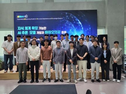
On May 23rd, KAIST (President Kwang-Hyung Lee) announced that its Digital Bio-Health AI Research Center (Director: Professor JongChul Ye of KAIST Kim Jaechul Graduate School of AI) has been selected for the Ministry of Science and ICT's 'AI Top-Tier Young Researcher Support Program (AI Star Fellowship Project).' With a total investment of ₩11.5 billion from May 2025 to December 2030, the center will embark on the full-scale development of AI technology and a platform capable of independently inferring and determining the kinds of diseases, and discovering new drugs.
< Photo. On May 20th, a kick-off meeting for the AI Star Fellowship Project was held at KAIST Kim Jaechul Graduate School of AI’s Yangjae Research Center with the KAIST research team and participating organizations of Samsung Medical Center, NAVER Cloud, and HITS. [From left to right in the front row] Professor Jaegul Joo (KAIST), Professor Yoonjae Choi (KAIST), Professor Woo Youn Kim (KAIST/HITS), Professor JongChul Ye (KAIST), Professor Sungsoo Ahn (KAIST), Dr. Haanju Yoo (NAVER Cloud), Yoonho Lee (KAIST), HyeYoon Moon (Samsung Medical Center), Dr. Su Min Kim (Samsung Medical Center) >
This project aims to foster an innovative AI research ecosystem centered on young researchers and develop an inferential AI agent that can utilize and automatically expand specialized knowledge systems in the bio and medical fields.
Professor JongChul Ye of the Kim Jaechul Graduate School of AI will serve as the lead researcher, with young researchers from KAIST including Professors Yoonjae Choi, Kimin Lee, Sungsoo Ahn, and Chanyoung Park, along with mid-career researchers like Professors Jaegul Joo and Woo Youn Kim, jointly undertaking the project. They will collaborate with various laboratories within KAIST to conduct comprehensive research covering the entire cycle from the theoretical foundations of AI inference to its practical application.
Specifically, the main goals include: - Building high-performance inference models that integrate diverse medical knowledge systems to enhance the precision and reliability of diagnosis and treatment. - Developing a convergence inference platform that efficiently combines symbol-based inference with neural network models. - Securing AI technology for new drug development and biomarker discovery based on 'cell ontology.'
Furthermore, through close collaboration with industry and medical institutions such as Samsung Medical Center, NAVER Cloud, and HITS Co., Ltd., the project aims to achieve: - Clinical diagnostic AI utilizing medical knowledge systems. - AI-based molecular target exploration for new drug development. - Commercialization of an extendible AI inference platform.
Professor JongChul Ye, Director of KAIST's Digital Bio-Health AI Research Center, stated, "At a time when competition in AI inference model development is intensifying, it is a great honor for KAIST to lead the development of AI technology specialized in the bio and medical fields with world-class young researchers." He added, "We will do our best to ensure that the participating young researchers reach a world-leading level in terms of research achievements after the completion of this seven-year project starting in 2025."
The AI Star Fellowship is a newly established program where post-doctoral researchers and faculty members within seven years of appointment participate as project leaders (PLs) to independently lead research. Multiple laboratories within a university and demand-side companies form a consortium to operate the program.
Through this initiative, KAIST plans to nurture bio-medical convergence AI talent and simultaneously promote the commercialization of core technologies in collaboration with Samsung Medical Center, NAVER Cloud, and HITS.
2025.05.26 View 3348
KAIST to Develop a Korean-style ChatGPT Platform Specifically Geared Toward Medical Diagnosis and Drug Discovery
On May 23rd, KAIST (President Kwang-Hyung Lee) announced that its Digital Bio-Health AI Research Center (Director: Professor JongChul Ye of KAIST Kim Jaechul Graduate School of AI) has been selected for the Ministry of Science and ICT's 'AI Top-Tier Young Researcher Support Program (AI Star Fellowship Project).' With a total investment of ₩11.5 billion from May 2025 to December 2030, the center will embark on the full-scale development of AI technology and a platform capable of independently inferring and determining the kinds of diseases, and discovering new drugs.
< Photo. On May 20th, a kick-off meeting for the AI Star Fellowship Project was held at KAIST Kim Jaechul Graduate School of AI’s Yangjae Research Center with the KAIST research team and participating organizations of Samsung Medical Center, NAVER Cloud, and HITS. [From left to right in the front row] Professor Jaegul Joo (KAIST), Professor Yoonjae Choi (KAIST), Professor Woo Youn Kim (KAIST/HITS), Professor JongChul Ye (KAIST), Professor Sungsoo Ahn (KAIST), Dr. Haanju Yoo (NAVER Cloud), Yoonho Lee (KAIST), HyeYoon Moon (Samsung Medical Center), Dr. Su Min Kim (Samsung Medical Center) >
This project aims to foster an innovative AI research ecosystem centered on young researchers and develop an inferential AI agent that can utilize and automatically expand specialized knowledge systems in the bio and medical fields.
Professor JongChul Ye of the Kim Jaechul Graduate School of AI will serve as the lead researcher, with young researchers from KAIST including Professors Yoonjae Choi, Kimin Lee, Sungsoo Ahn, and Chanyoung Park, along with mid-career researchers like Professors Jaegul Joo and Woo Youn Kim, jointly undertaking the project. They will collaborate with various laboratories within KAIST to conduct comprehensive research covering the entire cycle from the theoretical foundations of AI inference to its practical application.
Specifically, the main goals include: - Building high-performance inference models that integrate diverse medical knowledge systems to enhance the precision and reliability of diagnosis and treatment. - Developing a convergence inference platform that efficiently combines symbol-based inference with neural network models. - Securing AI technology for new drug development and biomarker discovery based on 'cell ontology.'
Furthermore, through close collaboration with industry and medical institutions such as Samsung Medical Center, NAVER Cloud, and HITS Co., Ltd., the project aims to achieve: - Clinical diagnostic AI utilizing medical knowledge systems. - AI-based molecular target exploration for new drug development. - Commercialization of an extendible AI inference platform.
Professor JongChul Ye, Director of KAIST's Digital Bio-Health AI Research Center, stated, "At a time when competition in AI inference model development is intensifying, it is a great honor for KAIST to lead the development of AI technology specialized in the bio and medical fields with world-class young researchers." He added, "We will do our best to ensure that the participating young researchers reach a world-leading level in terms of research achievements after the completion of this seven-year project starting in 2025."
The AI Star Fellowship is a newly established program where post-doctoral researchers and faculty members within seven years of appointment participate as project leaders (PLs) to independently lead research. Multiple laboratories within a university and demand-side companies form a consortium to operate the program.
Through this initiative, KAIST plans to nurture bio-medical convergence AI talent and simultaneously promote the commercialization of core technologies in collaboration with Samsung Medical Center, NAVER Cloud, and HITS.
2025.05.26 View 3348 -
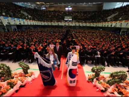 KAIST Holds 2025 Commencement Ceremony
KAIST (President Kwang-Hyung Lee) held its 2025 Commencement Ceremony at the Lyu Keun-Chul Sports Complex on the Daejeon Main Campus at 2 p.m. on the 14th of February.
< A scene from KAIST Commencement 2025 - Guests of Honor and Administrative Professors Entering the Stage headed by the color guards of the ELKA (Encouraging Leaders of KAIST) >
At this ceremony, a total of 3,144 degrees were conferred, including 785 doctorates, 1,643 masters, and 716 bachelors. With this, KAIST has produced a total of 81,156 advanced science and technology personnel, including 17,313 doctorates, 41,566 masters, and 22,277 bachelors since its establishment in 1971.
Changyu Lee from the School of Computing received the Minister of Science and ICT Award, and the Chairman of the KAIST Board of Trustees Award went to Lance Khizner Dabu Gragasin, an international student from the Philippines of the Department of Chemical and Biological Engineering. The President’s Award was given to Seoyeong Yang of the Department of Biological Sciences, and the Alumni Association President’s Award and the Development Foundation Chairman’s Award was given to Gahyeon Bae of the Department of Industrial Design and Buyeon Kim of the Department of Mechanical Engineering, respectively.
Minister of Science and ICT Sang-Im Yoo joined the ceremony to deliver a congratulatory speech and to present the awards to outstanding graduates.
< Minister Sang-Im Yoo of the Ministry of Science, Technology and ICT giving his congratulatory message at KAIST Commencement 2025 >
The valedictorian speeches were given by Minjae Kim of the School of Computing, who has practiced the value of sharing that learning is not competition but cooperation, and Mohammed Haruna Hamza of the Department of Aerospace Engineering, a Nigerian international student. Mr. Hamza is the first foreign student to represent the graduating class as valedictorian since the founding of KAIST.
Hamza lost his home and school in his home country due to a terrorist group’s bombing and moved south, but despite the adversity, he continued his studies while pursuing his dream of becoming an aerospace engineer. As a result of his efforts, Hamza was invited by the Korean government to study at KAIST. He expressed his determination to pursue his dream by saying, “I am grateful for the people and experiences that helped me overcome my adversity. The future is the result of the decisions we make today.”
A Pakistani international student was chosen as one of this year's "Most Talked about Graduates of the Year". It is Ali Syed Sheraz who wore his doctoral cap at this year’s commencement ceremony. Ali, a single father who left his one-year-old son behind in his home country, working as a university lecturer. He joined the Ph.D. program in mechanical engineering in 2019 with a passion for mechanical energy.
Ali’s academic journey was full of challenges and growth. Due to COVID-19, his research was suspended for six months, and he had difficulty continuing his studies undergoing three surgeries after a bicycle accident, including a surgery for a fractured elbow, a nose surgery, and removal of kidney stones.
However, he accepted these failure and hardship as a process of growth and participated in the ‘Failed Project Showcase’ and ‘Failure Essay Contest’ held by the KAIST Failure Society, sharing his experiences and growing into a more solid researcher.
< Most Talked about Graduate Graduate of the Year - Syed Sheraz Ali >
Despite experiencing various hardships, he found lessons to learn from them and changed his perspective, which made him unafraid of taking on new challenges. He showed through his own example that failure is not just stumbling blocks but can be a stepping stone to success by looking at his studies and personal life positively.
Furthermore, after becoming the president of the Muslim Student Association, Ali introduced halal menus to the cafeteria on campus so that more Muslim students could eat comfortably. Thanks to this change, his time at KAIST has become an opportunity to understand and experience various cultures more.
Ali is researching artificial muscles (soft actuators) with the world's highest bending strain using MXene, an artificial muscle nanomaterial that can move smoothly, in Professor Il-kwon Oh's lab.
Ali said, "After completing my Ph.D., I plan to develop soft robots, healthcare electronics, and next-generation tactile technology based on MXene, a next-generation 2D material. It is important for my juniors not to be afraid of failure and to have a challenging attitude."
Another 'Most Talked about Graduate of the Year', Mr. Sung-Hyun Jung, who graduated with a master's degree from the Graduate School of Bio Innvation Management, is the CEO of Promedius, a medical AI startup, and has commercialized an osteoporosis diagnosis software based on chest X-rays using AI, and grown it into a leading company in the bone health field.
CEO Jung's challenge shows that KAIST's management education is not just theoretical but practical enough to be applied immediately in the field. CEO Jung, who is also the father of three daughters, experienced business failure in China during the period when the conflict between Korea and China was intensifying.
He moved to Silicon Valley in the United States to revive his business and tried to acquire even small businesses, but the reality was not easy. He worked hard, standing 14 hours a day in a kimchi factory and a restaurant kitchen to make a living. After finishing his life in the United States, CEO Jung returned to Korea and had the opportunity to join Lunit, a global medical AI leader founded by KAIST graduates. CEO Jung experienced the growth of the global medical AI market firsthand with unit Chairman Seungwook Paek.
When he entered the Master's Program at the Graduate School of Bio Innvation Management in 2023 to acquire more specialized knowledge, CEO Jung had just transferred to Promedius and was in a crisis situation with only about 6 months left before the company's funds were exhausted.
While considering a change in business direction because he judged that it would be difficult to survive with existing business items, he learned keywords and investment review perspectives that venture capital (VC) pays attention to in Professor Hoonje Cho’s ‘Bio-innovation Business Startup Strategy and Practice’ class. He attracted 11.4 billion won in investment by applying the investment proposal he wrote based on what he learned from the class to actual practice.
< Most Talked about Graduate of the Year - Sung-Hyun Jung >
In addition, he applied the innovation strategy in the medical field he learned in Professor Kihwan Park’s ‘Innovation and Marketing in Bio and Pharmaceutics’ to the field of osteoporosis, and achieved the result of being selected as the first Asian company to be a corporate advisory committee member of the International Osteoporosis Foundation (IOF). Through this, he established the company as a representative global entity in the osteoporosis field in just one year.
CEO Jung, who applied what he learned from KAIST to actual management and achieved results in the global market in a short period of time, said, “I want to prove that KAIST education is not limited to theory, but is very practical.” He said, “I want to let people know that my life, once full of hardship, got on the track toward success after encountering KAIST,” and expressed his ambition, saying, “My long-term goal is to create a world-class company that is recognized globally.”
In addition, an honorary doctorate was awarded to Chairman Joong Keun Lee of Booyoung Group at the commencement ceremony.
Chairman Joong Keun Lee, who is an entrepreneur that led Booyoung Group, a leading general construction company, received the honorary doctorate in business administration, for leading the development of domestic housing welfare, education, and culture.
KAIST Provost Gyunmin Lee said, “Chairman Joong Keun Lee spared no effort in providing dedicated support for the development of domestic science and technology and the cultivation of future talents. He is awarded the honorary doctorate in recognition of his social responsibility in various fields, including scholarships and support for educational facilities, as well as domestic and international education, culture, veterans affairs, and overseas support.”
Since founding Booyoung Group in 1983, Chairman Lee has boldly entered the rental housing business, a field that large construction companies had avoided, and has played a significant role in improving the quality of life of ordinary citizens by supplying 230,000 households out of 383 complexes and approximately 300,000 households nationwide as rental housing, thereby contributing greatly to the stability of national housing.
< Chairman Joong Keun Lee giving his acceptance speech for his honorary Doctorate >
Chairman Joong Keun Lee, who has been offering hope for a sustainable future, said, “I am honored to receive an honorary doctorate from KAIST, and I hope that KAIST students will nurture their dreams and talents and grow into global talents who will contribute to national development.”
President Kwang-Hyung Lee said, “Chairman Joong Keun Lee has been carrying out various social contribution activities, and in particular, through supporting academic infrastructure, which is the core of national competitiveness, we can see his deep interest in and sense of responsibility for the development of science and technology in our country.” He added, “I am truly delighted to have him as a member of the KAIST family, and I congratulate him on behalf of all members, including our students.”
President Kwang-Hyung Lee also delivered a message of encouragement at the ceremony to charge the graduates to, “Find and keep a dream of your own, be on the lookout for opportunities, don’t be afraid of making mistakes, and do not shy away from taking on challenging tasks.” He added, “Even if you fail, don’t give up. Keep on trying so that you will get to that stage of radiate your own light on the stages where anything is possible.” (End)
2025.02.14 View 6140
KAIST Holds 2025 Commencement Ceremony
KAIST (President Kwang-Hyung Lee) held its 2025 Commencement Ceremony at the Lyu Keun-Chul Sports Complex on the Daejeon Main Campus at 2 p.m. on the 14th of February.
< A scene from KAIST Commencement 2025 - Guests of Honor and Administrative Professors Entering the Stage headed by the color guards of the ELKA (Encouraging Leaders of KAIST) >
At this ceremony, a total of 3,144 degrees were conferred, including 785 doctorates, 1,643 masters, and 716 bachelors. With this, KAIST has produced a total of 81,156 advanced science and technology personnel, including 17,313 doctorates, 41,566 masters, and 22,277 bachelors since its establishment in 1971.
Changyu Lee from the School of Computing received the Minister of Science and ICT Award, and the Chairman of the KAIST Board of Trustees Award went to Lance Khizner Dabu Gragasin, an international student from the Philippines of the Department of Chemical and Biological Engineering. The President’s Award was given to Seoyeong Yang of the Department of Biological Sciences, and the Alumni Association President’s Award and the Development Foundation Chairman’s Award was given to Gahyeon Bae of the Department of Industrial Design and Buyeon Kim of the Department of Mechanical Engineering, respectively.
Minister of Science and ICT Sang-Im Yoo joined the ceremony to deliver a congratulatory speech and to present the awards to outstanding graduates.
< Minister Sang-Im Yoo of the Ministry of Science, Technology and ICT giving his congratulatory message at KAIST Commencement 2025 >
The valedictorian speeches were given by Minjae Kim of the School of Computing, who has practiced the value of sharing that learning is not competition but cooperation, and Mohammed Haruna Hamza of the Department of Aerospace Engineering, a Nigerian international student. Mr. Hamza is the first foreign student to represent the graduating class as valedictorian since the founding of KAIST.
Hamza lost his home and school in his home country due to a terrorist group’s bombing and moved south, but despite the adversity, he continued his studies while pursuing his dream of becoming an aerospace engineer. As a result of his efforts, Hamza was invited by the Korean government to study at KAIST. He expressed his determination to pursue his dream by saying, “I am grateful for the people and experiences that helped me overcome my adversity. The future is the result of the decisions we make today.”
A Pakistani international student was chosen as one of this year's "Most Talked about Graduates of the Year". It is Ali Syed Sheraz who wore his doctoral cap at this year’s commencement ceremony. Ali, a single father who left his one-year-old son behind in his home country, working as a university lecturer. He joined the Ph.D. program in mechanical engineering in 2019 with a passion for mechanical energy.
Ali’s academic journey was full of challenges and growth. Due to COVID-19, his research was suspended for six months, and he had difficulty continuing his studies undergoing three surgeries after a bicycle accident, including a surgery for a fractured elbow, a nose surgery, and removal of kidney stones.
However, he accepted these failure and hardship as a process of growth and participated in the ‘Failed Project Showcase’ and ‘Failure Essay Contest’ held by the KAIST Failure Society, sharing his experiences and growing into a more solid researcher.
< Most Talked about Graduate Graduate of the Year - Syed Sheraz Ali >
Despite experiencing various hardships, he found lessons to learn from them and changed his perspective, which made him unafraid of taking on new challenges. He showed through his own example that failure is not just stumbling blocks but can be a stepping stone to success by looking at his studies and personal life positively.
Furthermore, after becoming the president of the Muslim Student Association, Ali introduced halal menus to the cafeteria on campus so that more Muslim students could eat comfortably. Thanks to this change, his time at KAIST has become an opportunity to understand and experience various cultures more.
Ali is researching artificial muscles (soft actuators) with the world's highest bending strain using MXene, an artificial muscle nanomaterial that can move smoothly, in Professor Il-kwon Oh's lab.
Ali said, "After completing my Ph.D., I plan to develop soft robots, healthcare electronics, and next-generation tactile technology based on MXene, a next-generation 2D material. It is important for my juniors not to be afraid of failure and to have a challenging attitude."
Another 'Most Talked about Graduate of the Year', Mr. Sung-Hyun Jung, who graduated with a master's degree from the Graduate School of Bio Innvation Management, is the CEO of Promedius, a medical AI startup, and has commercialized an osteoporosis diagnosis software based on chest X-rays using AI, and grown it into a leading company in the bone health field.
CEO Jung's challenge shows that KAIST's management education is not just theoretical but practical enough to be applied immediately in the field. CEO Jung, who is also the father of three daughters, experienced business failure in China during the period when the conflict between Korea and China was intensifying.
He moved to Silicon Valley in the United States to revive his business and tried to acquire even small businesses, but the reality was not easy. He worked hard, standing 14 hours a day in a kimchi factory and a restaurant kitchen to make a living. After finishing his life in the United States, CEO Jung returned to Korea and had the opportunity to join Lunit, a global medical AI leader founded by KAIST graduates. CEO Jung experienced the growth of the global medical AI market firsthand with unit Chairman Seungwook Paek.
When he entered the Master's Program at the Graduate School of Bio Innvation Management in 2023 to acquire more specialized knowledge, CEO Jung had just transferred to Promedius and was in a crisis situation with only about 6 months left before the company's funds were exhausted.
While considering a change in business direction because he judged that it would be difficult to survive with existing business items, he learned keywords and investment review perspectives that venture capital (VC) pays attention to in Professor Hoonje Cho’s ‘Bio-innovation Business Startup Strategy and Practice’ class. He attracted 11.4 billion won in investment by applying the investment proposal he wrote based on what he learned from the class to actual practice.
< Most Talked about Graduate of the Year - Sung-Hyun Jung >
In addition, he applied the innovation strategy in the medical field he learned in Professor Kihwan Park’s ‘Innovation and Marketing in Bio and Pharmaceutics’ to the field of osteoporosis, and achieved the result of being selected as the first Asian company to be a corporate advisory committee member of the International Osteoporosis Foundation (IOF). Through this, he established the company as a representative global entity in the osteoporosis field in just one year.
CEO Jung, who applied what he learned from KAIST to actual management and achieved results in the global market in a short period of time, said, “I want to prove that KAIST education is not limited to theory, but is very practical.” He said, “I want to let people know that my life, once full of hardship, got on the track toward success after encountering KAIST,” and expressed his ambition, saying, “My long-term goal is to create a world-class company that is recognized globally.”
In addition, an honorary doctorate was awarded to Chairman Joong Keun Lee of Booyoung Group at the commencement ceremony.
Chairman Joong Keun Lee, who is an entrepreneur that led Booyoung Group, a leading general construction company, received the honorary doctorate in business administration, for leading the development of domestic housing welfare, education, and culture.
KAIST Provost Gyunmin Lee said, “Chairman Joong Keun Lee spared no effort in providing dedicated support for the development of domestic science and technology and the cultivation of future talents. He is awarded the honorary doctorate in recognition of his social responsibility in various fields, including scholarships and support for educational facilities, as well as domestic and international education, culture, veterans affairs, and overseas support.”
Since founding Booyoung Group in 1983, Chairman Lee has boldly entered the rental housing business, a field that large construction companies had avoided, and has played a significant role in improving the quality of life of ordinary citizens by supplying 230,000 households out of 383 complexes and approximately 300,000 households nationwide as rental housing, thereby contributing greatly to the stability of national housing.
< Chairman Joong Keun Lee giving his acceptance speech for his honorary Doctorate >
Chairman Joong Keun Lee, who has been offering hope for a sustainable future, said, “I am honored to receive an honorary doctorate from KAIST, and I hope that KAIST students will nurture their dreams and talents and grow into global talents who will contribute to national development.”
President Kwang-Hyung Lee said, “Chairman Joong Keun Lee has been carrying out various social contribution activities, and in particular, through supporting academic infrastructure, which is the core of national competitiveness, we can see his deep interest in and sense of responsibility for the development of science and technology in our country.” He added, “I am truly delighted to have him as a member of the KAIST family, and I congratulate him on behalf of all members, including our students.”
President Kwang-Hyung Lee also delivered a message of encouragement at the ceremony to charge the graduates to, “Find and keep a dream of your own, be on the lookout for opportunities, don’t be afraid of making mistakes, and do not shy away from taking on challenging tasks.” He added, “Even if you fail, don’t give up. Keep on trying so that you will get to that stage of radiate your own light on the stages where anything is possible.” (End)
2025.02.14 View 6140 -
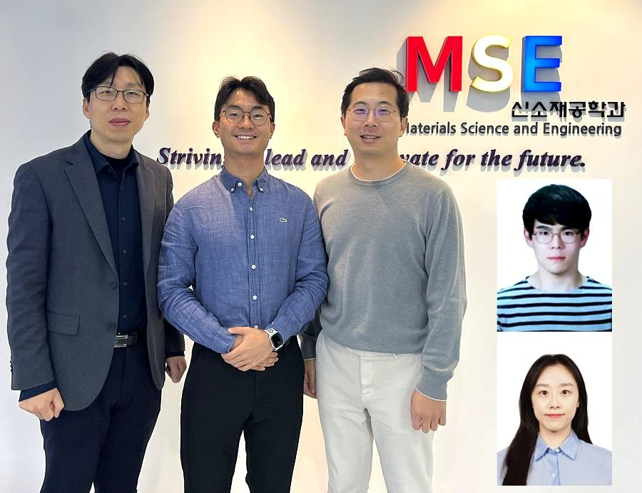 KAIST Develops CamBio - a New Biotemplating Method
- Professor Jae-Byum Chang and Professor Yeon Sik Jung’s joint research team of the Department of Materials Science and Engineering developed a highly tunable bio-templating method “CamBio” that makes use of intracellular protein structures
- Substrate performance improvement of up to 230% demonstrated via surface-enhanced Raman spectroscopy (SERS)
- Expected to have price competitiveness over bio-templating method as it expands the range of biological samples
- Expected to expand the range of application of nanostructure synthesis technology by utilizing various biological structures
< Photo 1. (From left) Professor Yeon Sik Jung, Ph.D. candidate Dae-Hyeon Song, Professor Jae-Byum Chang, and (from top right) Dr. Chang Woo Song and Dr. Seunghee H. Cho of the Department of Materials Science and Engineering >
Biological structures have complex characteristics that are difficult to replicate artificially, but biotemplating methods* that directly utilize these biological structures have been used in various fields of application. The KAIST research team succeeded in utilizing previously unusable biological structures and expanding the areas in which biotemplate methods can be applied.
*Biotemplating: A method of using biotemplates as a mold to create functional structural materials, utilizing the functions of these biological structures, from viruses to the tissues and organs that make up our bodies
KAIST (President Kwang Hyung Lee) announced on the 10th that a joint research team of Professors Jae-Byum Chang and Professor Yeon Sik Jung of the Department of Materials Science and Engineering developed a biotemplating method that utilizes specific intracellular proteins in biological samples and has high tunability.
Existing biotemplate methods mainly utilize only the external surface of biological samples or have limitations in utilizing the structure-function correlation of various biological structures due to limited dimensions and sample sizes, making it difficult to create functional nanostructures.
To solve this problem, the research team studied a way to utilize various biological structures within the cells while retaining high tunability.
< Figure 1. CamBio utilizing microtubules, a intracellular protein structure. The silver nanoparticle chains synthesized along the microtubules that span the entire cell interior can be observed through an electron microscope, and it is shown that this can be used as a successful SERS substrate. >
As a result of the research, the team developed the “Conversion to advanced materials via labeled Biostructure”, shortened as “CamBio”, which enables the selective synthesis of nanostructures with various characteristics and sizes from specific protein structures composed of diverse proteins within biological specimens.
The CamBio method secures high tunability of functional nanostructures that can be manufactured from biological samples by merging various manufacturing and biological technologies.
Through the technology of repeatedly attaching antibodies, arranging cells in a certain shape, and thinly slicing tissue, the functional nanostructures made with CamBio showed improved performance on the surface-enhanced Raman spectroscopy (SERS)* substrate used for material detection.
*Surface-enhanced Raman spectroscopy (SERS): A technology that can detect very small amounts of substances using light, based on the principle that specific substances react to light and amplifies signals on surfaces of metals such as gold or silver.
The research team found that the nanoparticle chains made using the intracellular protein structures through the process of repeated labeling with antibodies allowed easier control, and improved SERS performance by up to 230%.
In addition, the research team expanded from utilizing the structures inside cells to obtaining samples of muscle tissues inside meat using a cryostat and successfully producing a substrate with periodic bands made of metal particles by performing the CamBio process. This method of producing a substrate not only allows large-scale production using biological samples, but also shows that it is a cost-effective method.
< Figure 2. A method for securing tunability using CamBio at the cell level. Examples of controlling characteristics by integrating iterative labeling and cell pattering techniques with CamBio are shown. >
The CamBio developed by the research team is expected to be used as a way to solve problems faced by various research fields as it is to expand the range of bio-samples that can be produced for various usage.
The first author, Dae-Hyeon Song, a Ph.D. candidate of KAIST Department of Materials Science and Engineering said, “Through CamBio, we have comprehensively accumulated biotemplating methods that can utilize more diverse protein structures,” and “If combined with the state-of-the-art biological technologies such as gene editing and 3D bioprinting and new material synthesis technologies, biostructures can be utilized in various fields of application.”
< Figure 3. A method for securing tunability using CamBio at the tissue level. In order to utilize proteins inside muscle tissue, the frozen tissue sectioning technology is combined, and through this, a substrate with a periodic nanoparticle band pattern is successfully produced, and it is shown that large-area acquisition of samples and price competitiveness can be achieved. >
This study, in which the Ph.D. candidate Dae-Hyeon Song along with Dr. Chang Woo Song, and Dr. Seunghee H. Cho of the same department participated as the first authors, was published online in the international academic journal, Advanced Science, on November 13th, 2024.
(Paper title: Highly Tunable, Nanomaterial-Functionalized Structural Templating of Intracellular Protein Structures Within Biological Species) https://doi.org/10.1002/advs.202406492
This study was conducted with a combination of support from various programs including the National Convergence Research of Scientific Challenges (National Research Foundation of Korea (NRF) 2024), Engineering Reseach Center (ERC) (Wearable Platform Materials Technology Center, NRF 2023), ERC (Global Bio-integrated Materials Center, NRF 2024), and the National Advanced Program for Biological Research Resources (Bioimaging Data Curation Center, NRF 2024) funded by Ministry of Science and ICT.
2025.01.10 View 5084
KAIST Develops CamBio - a New Biotemplating Method
- Professor Jae-Byum Chang and Professor Yeon Sik Jung’s joint research team of the Department of Materials Science and Engineering developed a highly tunable bio-templating method “CamBio” that makes use of intracellular protein structures
- Substrate performance improvement of up to 230% demonstrated via surface-enhanced Raman spectroscopy (SERS)
- Expected to have price competitiveness over bio-templating method as it expands the range of biological samples
- Expected to expand the range of application of nanostructure synthesis technology by utilizing various biological structures
< Photo 1. (From left) Professor Yeon Sik Jung, Ph.D. candidate Dae-Hyeon Song, Professor Jae-Byum Chang, and (from top right) Dr. Chang Woo Song and Dr. Seunghee H. Cho of the Department of Materials Science and Engineering >
Biological structures have complex characteristics that are difficult to replicate artificially, but biotemplating methods* that directly utilize these biological structures have been used in various fields of application. The KAIST research team succeeded in utilizing previously unusable biological structures and expanding the areas in which biotemplate methods can be applied.
*Biotemplating: A method of using biotemplates as a mold to create functional structural materials, utilizing the functions of these biological structures, from viruses to the tissues and organs that make up our bodies
KAIST (President Kwang Hyung Lee) announced on the 10th that a joint research team of Professors Jae-Byum Chang and Professor Yeon Sik Jung of the Department of Materials Science and Engineering developed a biotemplating method that utilizes specific intracellular proteins in biological samples and has high tunability.
Existing biotemplate methods mainly utilize only the external surface of biological samples or have limitations in utilizing the structure-function correlation of various biological structures due to limited dimensions and sample sizes, making it difficult to create functional nanostructures.
To solve this problem, the research team studied a way to utilize various biological structures within the cells while retaining high tunability.
< Figure 1. CamBio utilizing microtubules, a intracellular protein structure. The silver nanoparticle chains synthesized along the microtubules that span the entire cell interior can be observed through an electron microscope, and it is shown that this can be used as a successful SERS substrate. >
As a result of the research, the team developed the “Conversion to advanced materials via labeled Biostructure”, shortened as “CamBio”, which enables the selective synthesis of nanostructures with various characteristics and sizes from specific protein structures composed of diverse proteins within biological specimens.
The CamBio method secures high tunability of functional nanostructures that can be manufactured from biological samples by merging various manufacturing and biological technologies.
Through the technology of repeatedly attaching antibodies, arranging cells in a certain shape, and thinly slicing tissue, the functional nanostructures made with CamBio showed improved performance on the surface-enhanced Raman spectroscopy (SERS)* substrate used for material detection.
*Surface-enhanced Raman spectroscopy (SERS): A technology that can detect very small amounts of substances using light, based on the principle that specific substances react to light and amplifies signals on surfaces of metals such as gold or silver.
The research team found that the nanoparticle chains made using the intracellular protein structures through the process of repeated labeling with antibodies allowed easier control, and improved SERS performance by up to 230%.
In addition, the research team expanded from utilizing the structures inside cells to obtaining samples of muscle tissues inside meat using a cryostat and successfully producing a substrate with periodic bands made of metal particles by performing the CamBio process. This method of producing a substrate not only allows large-scale production using biological samples, but also shows that it is a cost-effective method.
< Figure 2. A method for securing tunability using CamBio at the cell level. Examples of controlling characteristics by integrating iterative labeling and cell pattering techniques with CamBio are shown. >
The CamBio developed by the research team is expected to be used as a way to solve problems faced by various research fields as it is to expand the range of bio-samples that can be produced for various usage.
The first author, Dae-Hyeon Song, a Ph.D. candidate of KAIST Department of Materials Science and Engineering said, “Through CamBio, we have comprehensively accumulated biotemplating methods that can utilize more diverse protein structures,” and “If combined with the state-of-the-art biological technologies such as gene editing and 3D bioprinting and new material synthesis technologies, biostructures can be utilized in various fields of application.”
< Figure 3. A method for securing tunability using CamBio at the tissue level. In order to utilize proteins inside muscle tissue, the frozen tissue sectioning technology is combined, and through this, a substrate with a periodic nanoparticle band pattern is successfully produced, and it is shown that large-area acquisition of samples and price competitiveness can be achieved. >
This study, in which the Ph.D. candidate Dae-Hyeon Song along with Dr. Chang Woo Song, and Dr. Seunghee H. Cho of the same department participated as the first authors, was published online in the international academic journal, Advanced Science, on November 13th, 2024.
(Paper title: Highly Tunable, Nanomaterial-Functionalized Structural Templating of Intracellular Protein Structures Within Biological Species) https://doi.org/10.1002/advs.202406492
This study was conducted with a combination of support from various programs including the National Convergence Research of Scientific Challenges (National Research Foundation of Korea (NRF) 2024), Engineering Reseach Center (ERC) (Wearable Platform Materials Technology Center, NRF 2023), ERC (Global Bio-integrated Materials Center, NRF 2024), and the National Advanced Program for Biological Research Resources (Bioimaging Data Curation Center, NRF 2024) funded by Ministry of Science and ICT.
2025.01.10 View 5084 -
 A KAIST Team Develops Face-Conforming LED Mask Showing 340% Improved Efficacy in Deep Skin Elasticity
- A KAIST research team led by Professor Keon Jae Lee has developed a deep skin-stimulating LED mask which has been verified in clinical trials to improve dermis elasticity by 340%.
< Figure 1. Overall concept of face-fit surface-lighting micro-LEDs (FSLED) mask. a. Optical image of the FSLED mask showing uniform surface-lighting. schematic illustration of the FSLED mask. The 2D to 3D transformation procedure b. Difference in cosmetic effect on deep skin elasticity, wrinkles, and sagging between FSLED mask and CLED mask. (improvement percentage in eight weeks) >
Conventional LED masks, with their rigid design, fail to conform closely to the skin's contours. This limitation causes substantial light reflection, with up to 90% reflected over a distance of 2 cm, reducing light penetration and limiting stimulation of the deep skin layers essential for effective skin rejuvenation.
To address these challenges, Professor Lee's team developed a face-conforming surface lighting micro-LED (FSLED) mask, which can provide uniform photostimulation to the dermis. The key technology lies in the mask's ability to deliver uniform light to deep skin tissues while maintaining a conformal skin attachment. This is achieved through a 3D origami structure, integrated with 3,770 micro-LEDs and flexible surface light-diffusion layer, minimizing the gaps between the light source and the skin.
In clinical trials involving 33 participants, the FSLED mask demonstrated a 340% improvement in deep skin elasticity compared to conventional LED masks, proving its efficacy in significantly reducing skin wrinkles, sagging and aging.
Professor Keon Jae Lee said, “The FSLED mask provides cosmetic benefits to the entire facial dermis without the side effects of low-temperature burns, making home-care anti-aging treatment that enhances the quality of human life possible. The product is being manufactured by Fronics, KAIST startup company, and will be distributed globally through Amorepacific's network, with sales starting in November.”
This result titled “Clinical Validation of Face-fit Surface-lighting Micro Light-emitting Diode Mask for Skin Anti-aging Treatment”, in which Min Seo Kim, a student of the Master-Doctorate integrated program, and Jaehun An, a Ph.D. candidate, in the Department of Materials Science and Engineering of KAIST, took part as co-first authors, was published in Advanced Materials on October 22nd, 2024 (DOI: 10.1002/adma.202411651).
Introductory Video: Face-conforming surface LED mask for skin anti-aging ( https://www.youtube.com/watch?v=kSccLwx8N_w )
2024.10.29 View 7564
A KAIST Team Develops Face-Conforming LED Mask Showing 340% Improved Efficacy in Deep Skin Elasticity
- A KAIST research team led by Professor Keon Jae Lee has developed a deep skin-stimulating LED mask which has been verified in clinical trials to improve dermis elasticity by 340%.
< Figure 1. Overall concept of face-fit surface-lighting micro-LEDs (FSLED) mask. a. Optical image of the FSLED mask showing uniform surface-lighting. schematic illustration of the FSLED mask. The 2D to 3D transformation procedure b. Difference in cosmetic effect on deep skin elasticity, wrinkles, and sagging between FSLED mask and CLED mask. (improvement percentage in eight weeks) >
Conventional LED masks, with their rigid design, fail to conform closely to the skin's contours. This limitation causes substantial light reflection, with up to 90% reflected over a distance of 2 cm, reducing light penetration and limiting stimulation of the deep skin layers essential for effective skin rejuvenation.
To address these challenges, Professor Lee's team developed a face-conforming surface lighting micro-LED (FSLED) mask, which can provide uniform photostimulation to the dermis. The key technology lies in the mask's ability to deliver uniform light to deep skin tissues while maintaining a conformal skin attachment. This is achieved through a 3D origami structure, integrated with 3,770 micro-LEDs and flexible surface light-diffusion layer, minimizing the gaps between the light source and the skin.
In clinical trials involving 33 participants, the FSLED mask demonstrated a 340% improvement in deep skin elasticity compared to conventional LED masks, proving its efficacy in significantly reducing skin wrinkles, sagging and aging.
Professor Keon Jae Lee said, “The FSLED mask provides cosmetic benefits to the entire facial dermis without the side effects of low-temperature burns, making home-care anti-aging treatment that enhances the quality of human life possible. The product is being manufactured by Fronics, KAIST startup company, and will be distributed globally through Amorepacific's network, with sales starting in November.”
This result titled “Clinical Validation of Face-fit Surface-lighting Micro Light-emitting Diode Mask for Skin Anti-aging Treatment”, in which Min Seo Kim, a student of the Master-Doctorate integrated program, and Jaehun An, a Ph.D. candidate, in the Department of Materials Science and Engineering of KAIST, took part as co-first authors, was published in Advanced Materials on October 22nd, 2024 (DOI: 10.1002/adma.202411651).
Introductory Video: Face-conforming surface LED mask for skin anti-aging ( https://www.youtube.com/watch?v=kSccLwx8N_w )
2024.10.29 View 7564 -
 A KAIST research team develops a washable, transparent, and flexible OLED with MXene nanotechnology
Transparent and flexible displays, which have received a lot of attention in various fields including automobile displays, bio-healthcare, military, and fashion, are in fact known to break easily when experiencing small deformations. To solve this problem, active research is being conducted on many transparent and flexible conductive materials such as carbon nanotubes, graphene, silver nanowires, and conductive polymers.
On June 13, a joint research team led by Professor Kyung Cheol Choi from the KAIST School of Electrical Engineering and Dr. Yonghee Lee from the National Nano Fab Center (NNFC) announced the successful development of a water-resistant, transparent, and flexible OLED using MXene nanotechnology. The material can emit and transmit light even when exposed to water.
MXene is a 2D material with high electrical conductivity and optical transmittance, and it can be produced on a large scale through solution processes. However, despite these attractive properties, MXene’s applications were limited as a long-term electrical device due to its electrical properties being degraded easily by atmospheric moisture and water. The material was therefore unable to be systemized into the form of a matrix that can display information.
Professor Choi’s research team used an encapsulation tactic that can protect materials from oxidation caused by moisture and oxygen to develop a MXene-based OLED with a long lifespan and high stability against external environmental factors. The research team first focused on analyzing the degradation mechanism of MXene’s electrical conductivity, and then concentrated on designing an encapsulation membrane. The team blocked moisture and provided flexibility through residual stress offset, ultimately producing a double-layered encapsulation membrane. In addition, a thin plastic film with a thickness of a few micrometers was attached to the top layer to allow washing in water without degradation.
< Figure 1. (a) Transparent passive-matrix display made of MXene-based OLED, (b) Cross-sectional image of MXene-based OLED observed by transmission electron microscope (TEM), (c) Electro-optical characteristic graph of red, green, and blue MXene-based OLED >
Through this study, the research team developed a MXene-based red(R)/green(G)/blue(B) OLED that emits a brightness of over 1,000 cd/m2 that is detectable by the naked eye even under sunlight, thereby meeting the conditions for outdoor displays. As for the red MXene-based OLED, the researchers confirmed a standby storage life of 2,000 hours (under 70% luminescence), a standby operation life of 1,500 hours (under 60% luminescence), and a flexibility withstanding 1,000 cycles under a low curvature of under 1.5mm. In addition, they showed that its performance was maintained even after six hours of immersion under water (under 80% luminescence). Furthermore, a patterning technique was used to produce the MXene-based OLED in the form of a passive matrix, and the team demonstrated its use as a transparent display by displaying letters and shapes.
Ph.D. candidate So Yeong Jeong, who led this study, said, “To improve the reliability of MXene OLED, we focused on producing an adequate encapsulation structure and a suitable process design.” She added, “By producing a matrix-type MXene OLED and displaying simple letters and shapes, we have laid the foundations for MXene’s application in the field of transparent displays.”
< Image 1. Cover of ACS Nano Front Cover (Conceptual diagram of MXene-based OLED display) >
Professor Choi said, “This research will become the guideline for applying MXene in electrical devices, but we expect for it to also be applied in other fields that require flexible and transparent displays like automobiles, fashion, and functional clothing. And to widen the gap with China’s OLED technology, these new OLED convergence technologies must continue to be developed.”
This research was supported by the National Research Foundation of Korea and funded by the Ministry of Science and ICT, Korea. It was published as a front cover story of ACS Nano under the title, “Highly Air-Stable, Flexible, and Water-Resistive 2D Titanium Carbide MXene-Based RGB Organic Light-Emitting Diode Displays for Transparent Free-Form Electronics” on June 13.
2023.07.10 View 7845
A KAIST research team develops a washable, transparent, and flexible OLED with MXene nanotechnology
Transparent and flexible displays, which have received a lot of attention in various fields including automobile displays, bio-healthcare, military, and fashion, are in fact known to break easily when experiencing small deformations. To solve this problem, active research is being conducted on many transparent and flexible conductive materials such as carbon nanotubes, graphene, silver nanowires, and conductive polymers.
On June 13, a joint research team led by Professor Kyung Cheol Choi from the KAIST School of Electrical Engineering and Dr. Yonghee Lee from the National Nano Fab Center (NNFC) announced the successful development of a water-resistant, transparent, and flexible OLED using MXene nanotechnology. The material can emit and transmit light even when exposed to water.
MXene is a 2D material with high electrical conductivity and optical transmittance, and it can be produced on a large scale through solution processes. However, despite these attractive properties, MXene’s applications were limited as a long-term electrical device due to its electrical properties being degraded easily by atmospheric moisture and water. The material was therefore unable to be systemized into the form of a matrix that can display information.
Professor Choi’s research team used an encapsulation tactic that can protect materials from oxidation caused by moisture and oxygen to develop a MXene-based OLED with a long lifespan and high stability against external environmental factors. The research team first focused on analyzing the degradation mechanism of MXene’s electrical conductivity, and then concentrated on designing an encapsulation membrane. The team blocked moisture and provided flexibility through residual stress offset, ultimately producing a double-layered encapsulation membrane. In addition, a thin plastic film with a thickness of a few micrometers was attached to the top layer to allow washing in water without degradation.
< Figure 1. (a) Transparent passive-matrix display made of MXene-based OLED, (b) Cross-sectional image of MXene-based OLED observed by transmission electron microscope (TEM), (c) Electro-optical characteristic graph of red, green, and blue MXene-based OLED >
Through this study, the research team developed a MXene-based red(R)/green(G)/blue(B) OLED that emits a brightness of over 1,000 cd/m2 that is detectable by the naked eye even under sunlight, thereby meeting the conditions for outdoor displays. As for the red MXene-based OLED, the researchers confirmed a standby storage life of 2,000 hours (under 70% luminescence), a standby operation life of 1,500 hours (under 60% luminescence), and a flexibility withstanding 1,000 cycles under a low curvature of under 1.5mm. In addition, they showed that its performance was maintained even after six hours of immersion under water (under 80% luminescence). Furthermore, a patterning technique was used to produce the MXene-based OLED in the form of a passive matrix, and the team demonstrated its use as a transparent display by displaying letters and shapes.
Ph.D. candidate So Yeong Jeong, who led this study, said, “To improve the reliability of MXene OLED, we focused on producing an adequate encapsulation structure and a suitable process design.” She added, “By producing a matrix-type MXene OLED and displaying simple letters and shapes, we have laid the foundations for MXene’s application in the field of transparent displays.”
< Image 1. Cover of ACS Nano Front Cover (Conceptual diagram of MXene-based OLED display) >
Professor Choi said, “This research will become the guideline for applying MXene in electrical devices, but we expect for it to also be applied in other fields that require flexible and transparent displays like automobiles, fashion, and functional clothing. And to widen the gap with China’s OLED technology, these new OLED convergence technologies must continue to be developed.”
This research was supported by the National Research Foundation of Korea and funded by the Ministry of Science and ICT, Korea. It was published as a front cover story of ACS Nano under the title, “Highly Air-Stable, Flexible, and Water-Resistive 2D Titanium Carbide MXene-Based RGB Organic Light-Emitting Diode Displays for Transparent Free-Form Electronics” on June 13.
2023.07.10 View 7845 -
 KAIST researchers devises a technology to utilize ultrahigh-resolution micro-LED with 40% reduced self-generated heat
In the digitized modern life, various forms of future displays, such as wearable and rollable displays are required. More and more people are wanting to connect to the virtual world whenever and wherever with the use of their smartglasses or smartwatches. Even further, we’ve been hearing about medical diagnosis kit on a shirt and a theatre-hat. However, it is not quite here in our hands yet due to technical limitations of being unable to fit as many pixels as a limited surface area of a glasses while keeping the power consumption at the a level that a hand held battery can supply, all the while the resolution of 4K+ is needed in order to perfectly immerse the users into the augmented or virtual reality through a wireless smartglasses or whatever the device.
KAIST (President Kwang Hyung Lee) announced on the 22nd that Professor Sang Hyeon Kim's research team of the Department of Electrical and Electronic Engineering re-examined the phenomenon of efficiency degradation of micro-LEDs with pixels in a size of micrometers (μm, one millionth of a meter) and found that it was possible to fundamentally resolve the problem by the use of epitaxial structure engineering.
Epitaxy refers to the process of stacking gallium nitride crystals that are used as a light emitting body on top of an ultrapure silicon or sapphire substrate used for μLEDs as a medium.
μLED is being actively studied because it has the advantages of superior brightness, contrast ratio, and lifespan compared to OLED. In 2018, Samsung Electronics commercialized a product equipped with μLED called 'The Wall'. And there is a prospect that Apple may be launching a μLED-mounted product in 2025.
In order to manufacture μLEDs, pixels are formed by cutting the epitaxial structure grown on a wafer into a cylinder or cuboid shape through an etching process, and this etching process is accompanied by a plasma-based process. However, these plasmas generate defects on the side of the pixel during the pixel formation process.
Therefore, as the pixel size becomes smaller and the resolution increases, the ratio of the surface area to the volume of the pixel increases, and defects on the side of the device that occur during processing further reduce the device efficiency of the μLED. Accordingly, a considerable amount of research has been conducted on mitigating or removing sidewall defects, but this method has a limit to the degree of improvement as it must be done at the post-processing stage after the grown of the epitaxial structure is finished.
The research team identified that there is a difference in the current moving to the sidewall of the μLED depending on the epitaxial structure during μLED device operation, and based on the findings, the team built a structure that is not sensitive to sidewall defects to solve the problem of reduced efficiency due to miniaturization of μLED devices. In addition, the proposed structure reduced the self-generated heat while the device was running by about 40% compared to the existing structure, which is also of great significance in commercialization of ultrahigh-resolution μLED displays.
This study, which was led by Woo Jin Baek of Professor Sang Hyeon Kim's research team at the KAIST School of Electrical and Electronic Engineering as the first author with guidance by Professor Sang Hyeon Kim and Professor Dae-Myeong Geum of the Chungbuk National University (who was with the team as a postdoctoral researcher at the time) as corresponding authors, was published in the international journal, 'Nature Communications' on March 17th. (Title of the paper: Ultra-low-current driven InGaN blue micro light-emitting diodes for electrically efficient and self-heating relaxed microdisplay).
Professor Sang Hyeon Kim said, "This technological development has great meaning in identifying the cause of the drop in efficiency, which was an obstacle to miniaturization of μLED, and solving it with the design of the epitaxial structure.“ He added, ”We are looking forward to it being used in manufacturing of ultrahigh-resolution displays in the future."
This research was carried out with the support of the Samsung Future Technology Incubation Center.
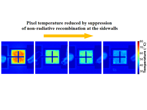
Figure 1. Image of electroluminescence distribution of μLEDs fabricated from epitaxial structures with quantum barriers of different thicknesses while the current is running
Figure 2. Thermal distribution images of devices fabricated with different epitaxial structures under the same amount of light.
Figure 3. Normalized external quantum efficiency of the device fabricated with the optimized epitaxial structure by sizes.
2023.03.23 View 8268
KAIST researchers devises a technology to utilize ultrahigh-resolution micro-LED with 40% reduced self-generated heat
In the digitized modern life, various forms of future displays, such as wearable and rollable displays are required. More and more people are wanting to connect to the virtual world whenever and wherever with the use of their smartglasses or smartwatches. Even further, we’ve been hearing about medical diagnosis kit on a shirt and a theatre-hat. However, it is not quite here in our hands yet due to technical limitations of being unable to fit as many pixels as a limited surface area of a glasses while keeping the power consumption at the a level that a hand held battery can supply, all the while the resolution of 4K+ is needed in order to perfectly immerse the users into the augmented or virtual reality through a wireless smartglasses or whatever the device.
KAIST (President Kwang Hyung Lee) announced on the 22nd that Professor Sang Hyeon Kim's research team of the Department of Electrical and Electronic Engineering re-examined the phenomenon of efficiency degradation of micro-LEDs with pixels in a size of micrometers (μm, one millionth of a meter) and found that it was possible to fundamentally resolve the problem by the use of epitaxial structure engineering.
Epitaxy refers to the process of stacking gallium nitride crystals that are used as a light emitting body on top of an ultrapure silicon or sapphire substrate used for μLEDs as a medium.
μLED is being actively studied because it has the advantages of superior brightness, contrast ratio, and lifespan compared to OLED. In 2018, Samsung Electronics commercialized a product equipped with μLED called 'The Wall'. And there is a prospect that Apple may be launching a μLED-mounted product in 2025.
In order to manufacture μLEDs, pixels are formed by cutting the epitaxial structure grown on a wafer into a cylinder or cuboid shape through an etching process, and this etching process is accompanied by a plasma-based process. However, these plasmas generate defects on the side of the pixel during the pixel formation process.
Therefore, as the pixel size becomes smaller and the resolution increases, the ratio of the surface area to the volume of the pixel increases, and defects on the side of the device that occur during processing further reduce the device efficiency of the μLED. Accordingly, a considerable amount of research has been conducted on mitigating or removing sidewall defects, but this method has a limit to the degree of improvement as it must be done at the post-processing stage after the grown of the epitaxial structure is finished.
The research team identified that there is a difference in the current moving to the sidewall of the μLED depending on the epitaxial structure during μLED device operation, and based on the findings, the team built a structure that is not sensitive to sidewall defects to solve the problem of reduced efficiency due to miniaturization of μLED devices. In addition, the proposed structure reduced the self-generated heat while the device was running by about 40% compared to the existing structure, which is also of great significance in commercialization of ultrahigh-resolution μLED displays.
This study, which was led by Woo Jin Baek of Professor Sang Hyeon Kim's research team at the KAIST School of Electrical and Electronic Engineering as the first author with guidance by Professor Sang Hyeon Kim and Professor Dae-Myeong Geum of the Chungbuk National University (who was with the team as a postdoctoral researcher at the time) as corresponding authors, was published in the international journal, 'Nature Communications' on March 17th. (Title of the paper: Ultra-low-current driven InGaN blue micro light-emitting diodes for electrically efficient and self-heating relaxed microdisplay).
Professor Sang Hyeon Kim said, "This technological development has great meaning in identifying the cause of the drop in efficiency, which was an obstacle to miniaturization of μLED, and solving it with the design of the epitaxial structure.“ He added, ”We are looking forward to it being used in manufacturing of ultrahigh-resolution displays in the future."
This research was carried out with the support of the Samsung Future Technology Incubation Center.
Figure 1. Image of electroluminescence distribution of μLEDs fabricated from epitaxial structures with quantum barriers of different thicknesses while the current is running
Figure 2. Thermal distribution images of devices fabricated with different epitaxial structures under the same amount of light.
Figure 3. Normalized external quantum efficiency of the device fabricated with the optimized epitaxial structure by sizes.
2023.03.23 View 8268 -
 KAIST researchers develops a tech to enable production of ultrahigh-resolution LED with sub-micrometer scale pixels
Ultrahigh-resolution displays are an essential element for developing next-generation electronic products such as virtual reality (VR), augmented reality (AR), and smart watches, and can be applied not only to head-mounted displays, but also to smart glasses and smart lenses. The technology developed through this research is expected to be used to make such next-generation ultrahigh-resolution displays and other various sub-micro optoelectronic devices.
KAIST (President Kwang Hyung Lee) announced on the 22nd that Professor Yong-Hoon Cho's research team of KAIST Department of Physics developed the core technology for an ultrahigh resolution light-emitting diode (LED) display that can realize 0.5 micron-scale pixels smaller than 1/100 of the average hair thickness (about 100 microns) using focused ion beams.
Commonly, pixelation of ultrahigh-resolution LED displays usually relies on the etching method that physically cuts the area around the pixel, but as the pixel becomes smaller due to the occurrence of various defects around it, leading to side-effects of having leakage of current increased and light-emission efficiency decreased. In addition, various complex processes such as patterning for pixelation and post-processing for prevention of leakage current are required.
Professor Yong-Hoon Cho's research team developed a technology that can create pixels down to the size of a microscale without the complicated pre- and post-processing using a focused ion beam. This method has the advantage of being able to freely set the shape of the emitting pixel without causing any structural deformation on the material surface by controlling the intensity of the focused ion beam.
The focused ion beam technology has been widely used for ultrahigh-magnification imaging and nanostructure fabrication in fields such as materials engineering and biology. However, when a focused ion beam is used on a light emitting body such as an LED, light emission of a portion hit by the beam and a surrounding area rapidly decreases, which has been a barrier to fabricating a nano-scale light emitting structure. Upon facing this issue, Professor Cho's research team began the research on the idea that if they turned things around to use these problematic phenomena, they can be used in ultra-fine pixelation method on a sub-micron scale.
The research team used a focused ion beam whose intensity was softened to the extent that the surface was not shaved, and found that not only the light-emission rapidly decreased in the area hit by the focused ion beam, but also the local resistance greatly increased. As a result, while the surface of the LED is kept flat, the portion hit by the focused ion beam is optically and electrically isolated, enabling pixelation for independent operation.
Professor Yong-Hoon Cho, who led the research, said, “We have newly developed a technology that can create sub-micron-scale pixels without complicated processes using a focused ion beam, which will be a base technology that can be applied to next-generation ultrahigh-resolution displays and nano-photoelectronic devices.”
This research in which the Master's student Ji-Hwan Moon and the Ph.D. student Baul Kim of KAIST Department of Physics participated as co-first authors, was carried out with the support of the National Research Foundation of Korea's Support Program for Mid-Career Researchers and the Institute of Information and Communications Technology Planning and Evaluation. It was published online in 'Advanced Materials' on February 13, and was also selected as the internal cover of the next offline edition. (Title: Electrically Driven Sub-Micron Light-Emitting Diode Arrays Using Maskless and Etching-Free Pixelation)
Figure 1. Schematic diagram of the technology for ultrahigh density sub-micron-sized pixels through He focused ion beam (FIB) irradiation on an LED device
Figure 2. Ultra-high-density pixelation technology of micro light-emitting diodes (μLED) through He focused ion beam (FIB) irradiation
Figure 3. Rectangular pixels of different sizes (surface structure picture and luminescence picture) realized by a focused ion beam. Luminescence pictures of pixel arrays ranging in size from 20 µm x 20 µm to 0.5 µm x 0.5 µm, with surface flatness maintained.
2023.03.08 View 8729
KAIST researchers develops a tech to enable production of ultrahigh-resolution LED with sub-micrometer scale pixels
Ultrahigh-resolution displays are an essential element for developing next-generation electronic products such as virtual reality (VR), augmented reality (AR), and smart watches, and can be applied not only to head-mounted displays, but also to smart glasses and smart lenses. The technology developed through this research is expected to be used to make such next-generation ultrahigh-resolution displays and other various sub-micro optoelectronic devices.
KAIST (President Kwang Hyung Lee) announced on the 22nd that Professor Yong-Hoon Cho's research team of KAIST Department of Physics developed the core technology for an ultrahigh resolution light-emitting diode (LED) display that can realize 0.5 micron-scale pixels smaller than 1/100 of the average hair thickness (about 100 microns) using focused ion beams.
Commonly, pixelation of ultrahigh-resolution LED displays usually relies on the etching method that physically cuts the area around the pixel, but as the pixel becomes smaller due to the occurrence of various defects around it, leading to side-effects of having leakage of current increased and light-emission efficiency decreased. In addition, various complex processes such as patterning for pixelation and post-processing for prevention of leakage current are required.
Professor Yong-Hoon Cho's research team developed a technology that can create pixels down to the size of a microscale without the complicated pre- and post-processing using a focused ion beam. This method has the advantage of being able to freely set the shape of the emitting pixel without causing any structural deformation on the material surface by controlling the intensity of the focused ion beam.
The focused ion beam technology has been widely used for ultrahigh-magnification imaging and nanostructure fabrication in fields such as materials engineering and biology. However, when a focused ion beam is used on a light emitting body such as an LED, light emission of a portion hit by the beam and a surrounding area rapidly decreases, which has been a barrier to fabricating a nano-scale light emitting structure. Upon facing this issue, Professor Cho's research team began the research on the idea that if they turned things around to use these problematic phenomena, they can be used in ultra-fine pixelation method on a sub-micron scale.
The research team used a focused ion beam whose intensity was softened to the extent that the surface was not shaved, and found that not only the light-emission rapidly decreased in the area hit by the focused ion beam, but also the local resistance greatly increased. As a result, while the surface of the LED is kept flat, the portion hit by the focused ion beam is optically and electrically isolated, enabling pixelation for independent operation.
Professor Yong-Hoon Cho, who led the research, said, “We have newly developed a technology that can create sub-micron-scale pixels without complicated processes using a focused ion beam, which will be a base technology that can be applied to next-generation ultrahigh-resolution displays and nano-photoelectronic devices.”
This research in which the Master's student Ji-Hwan Moon and the Ph.D. student Baul Kim of KAIST Department of Physics participated as co-first authors, was carried out with the support of the National Research Foundation of Korea's Support Program for Mid-Career Researchers and the Institute of Information and Communications Technology Planning and Evaluation. It was published online in 'Advanced Materials' on February 13, and was also selected as the internal cover of the next offline edition. (Title: Electrically Driven Sub-Micron Light-Emitting Diode Arrays Using Maskless and Etching-Free Pixelation)
Figure 1. Schematic diagram of the technology for ultrahigh density sub-micron-sized pixels through He focused ion beam (FIB) irradiation on an LED device
Figure 2. Ultra-high-density pixelation technology of micro light-emitting diodes (μLED) through He focused ion beam (FIB) irradiation
Figure 3. Rectangular pixels of different sizes (surface structure picture and luminescence picture) realized by a focused ion beam. Luminescence pictures of pixel arrays ranging in size from 20 µm x 20 µm to 0.5 µm x 0.5 µm, with surface flatness maintained.
2023.03.08 View 8729 -
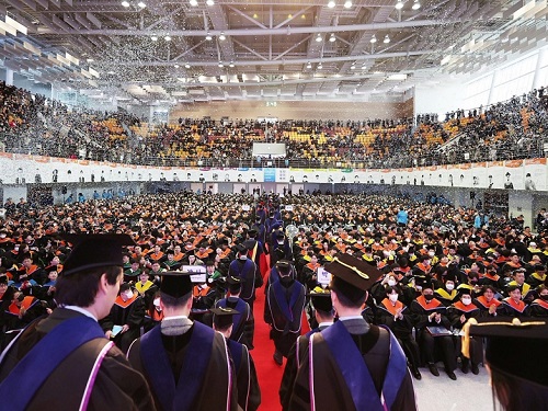 KAIST Holds 2023 Commencement Ceremony
< Photo 1. On the 17th, KAIST held the 2023 Commencement Ceremony for a total of 2,870 students, including 691 doctors. >
KAIST held its 2023 commencement ceremony at the Sports Complex of its main campus in Daejeon at 2 p.m. on February 27. It was the first commencement ceremony to invite all its graduates since the start of COVID-19 quarantine measures.
KAIST awarded a total of 2,870 degrees including 691 PhD degrees, 1,464 master’s degrees, and 715 bachelor’s degrees, which adds to the total of 74,999 degrees KAIST has conferred since its foundation in 1971, which includes 15,772 PhD, 38,360 master’s and 20,867 bachelor’s degrees.
This year’s Cum Laude, Gabin Ryu, from the Department of Mechanical Engineering received the Minister of Science and ICT Award. Seung-ju Lee from the School of Computing received the Chairman of the KAIST Board of Trustees Award, while Jantakan Nedsaengtip, an international student from Thailand received the KAIST Presidential Award, and Jaeyong Hwang from the Department of Physics and Junmo Lee from the Department of Industrial and Systems Engineering each received the President of the Alumni Association Award and the Chairman of the KAIST Development Foundation Award, respectively.
Minister Jong-ho Lee of the Ministry of Science and ICT awarded the recipients of the academic awards and delivered a congratulatory speech.
Yujin Cha from the Department of Bio and Brain Engineering, who received a PhD degree after 19 years since his entrance to KAIST as an undergraduate student in 2004 gave a speech on behalf of the graduates to move and inspire the graduates and the guests.
After Cha received a bachelor’s degree from the Department of Nuclear and Quantum Engineering, he entered a medical graduate school and became a radiation oncology specialist. But after experiencing the death of a young patient who suffered from osteosarcoma, he returned to his alma mater to become a scientist. As he believes that science and technology is the ultimate solution to the limitations of modern medicine, he started as a PhD student at the Department of Bio and Brain Engineering in 2018, hoping to find such solutions.
During his course, he identified the characteristics of the decision-making process of doctors during diagnosis, and developed a brain-inspired AI algorithm. It is an original and challenging study that attempted to develop a fundamental machine learning theory from the data he collected from 200 doctors of different specialties.
Cha said, “Humans and AI can cooperate by humans utilizing the unique learning abilities of AI to develop our expertise, while AIs can mimic us humans’ learning abilities to improve.” He added, “My ultimate goal is to develop technology to a level at which humans and machines influence each other and ‘coevolve’, and applying it not only to medicine, but in all areas.”
Cha, who is currently an assistant professor at the KAIST Biomedical Research Center, has also written Artificial Intelligence for Doctors in 2017 to help medical personnel use AI in clinical fields, and the book was selected as one of the 2018 Sejong Books in the academic category.
During his speech at this year’s commencement ceremony, he shared that “there are so many things in the world that are difficult to solve and many things to solve them with, but I believe the things that can really broaden the horizons of the world and find fundamental solutions to the problems at hand are science and technology.”
Meanwhile, singer-songwriter Sae Byul Park who studied at the KAIST Graduate School of Culture Technology will also receive her PhD degree.
Natural language processing (NLP) is a field in AI that teaches a computer to understand and analyze human language that is actively being studied. An example of NLP is ChatGTP, which recently received a lot of attention. For her research, Park analyzed music rather than language using NLP technology.
To analyze music, which is in the form of sound, using the methods for NLP, it is necessary to rebuild notes and beats into a form of words or sentences as in a language. For this, Park designed an algorithm called Mel2Word and applied it to her research.
She also suggested that by converting melodies into texts for analysis, one would be able to quantitatively express music as sentences or words with meaning and context rather than as simple sounds representing a certain note.
Park said, “music has always been considered as a product of subjective emotion, but this research provides a framework that can calculate and analyze music.”
Park’s study can later be developed into a tool to measure the similarities between musical work, as well as a piece’s originality, artistry and popularity, and it can be used as a clue to explore the fundamental principles of how humans respond to music from a cognitive science perspective.
Park began her Ph.D. program in 2014, while carrying on with her musical activities as well as public and university lectures alongside, and dealing with personally major events including marriage and childbirth during the course of years. She already met the requirements to receive her degree in 2019, but delayed her graduation in order to improve the level of completion of her research, and finally graduated with her current achievements after nine years.
Professor Juhan Nam, who supervised Park’s research, said, “Park, who has a bachelor’s degree in psychology, later learned to code for graduate school, and has complete high-quality research in the field of artificial intelligence.” He added, “Though it took a long time, her attitude of not giving up until the end as a researcher is also excellent.”
Sae Byul Park is currently lecturing courses entitled Culture Technology and Music Information Retrieval at the Underwood International College of Yonsei University.
Park said, “the 10 or so years I’ve spent at KAIST as a graduate student was a time I could learn and prosper not only academically but from all angles of life.” She added, “having received a doctorate degree is not the end, but a ‘commencement’. Therefore, I will start to root deeper from the seeds I sowed and work harder as a both a scholar and an artist.”
< Photo 2. From left) Yujin Cha (Valedictorian, Medical-Scientist Program Ph.D. graduate), Saebyeol Park (a singer-songwriter, Ph.D. graduate from the Graduate School of Culture and Technology), Junseok Moon and Inah Seo (the two highlighted CEO graduates from the Department of Management Engineering's master’s program) >
Young entrepreneurs who dream of solving social problems will also be wearing their graduation caps. Two such graduates are Jun-seok Moon and Inah Seo, receiving their master’s degrees in social entrepreneurship MBA from the KAIST College of Business.
Before entrance, Moon ran a café helping African refugees stand on their own feet. Then, he entered KAIST to later expand his business and learn social entrepreneurship in order to sustainably help refugees in the blind spots of human rights and welfare.
During his master’s course, Moon realized that he could achieve active carbon reduction by changing the coffee alone, and switched his business field and founded Equal Table. The amount of carbon an individual can reduce by refraining from using a single paper cup is 10g, while changing the coffee itself can reduce it by 300g.
1kg of coffee emits 15kg of carbon over the course of its production, distribution, processing, and consumption, but Moon produces nearly carbon-neutral coffee beans by having innovated the entire process. In particular, the company-to-company ESG business solution is Moon’s new start-up area. It provides companies with carbon-reduced coffee made by roasting raw beans from carbon-neutral certified farms with 100% renewable energy, and shows how much carbon has been reduced in its making. Equal Table will launch the service this month in collaboration with SK Telecom, its first partner.
Inah Seo, who also graduated with Moon, founded Conscious Wear to start a fashion business reducing environmental pollution. In order to realize her mission, she felt the need to gain the appropriate expertise in management, and enrolled for the social entrepreneurship MBA.
Out of the various fashion industries, Seo focused on the leather market, which is worth 80 trillion won. Due to thickness or contamination issues, only about 60% of animal skin fabric is used, and the rest is discarded. Heavy metals are used during such processes, which also directly affects the environment.
During the social entrepreneurship MBA course, Seo collaborated with SK Chemicals, which had links through the program, and launched eco-friendly leather bags. The bags used discarded leather that was recycled by grinding and reprocessing into a biomaterial called PO3G. It was the first case in which PO3G that is over 90% biodegradable was applied to regenerated leather. In other words, it can reduce environmental pollution in the processing and disposal stages, while also reducing carbon emissions and water usage by one-tenth compared to existing cowhide products.
The social entrepreneurship MBA course, from which Moon and Seo graduated, will run in integration with the Graduate School of Green Growth as an Impact MBA program starting this year. KAIST plans to steadily foster entrepreneurs who will lead meaningful changes in the environment and society as well as economic values through innovative technologies and ideas.
< Photo 3. NYU President Emeritus John Sexton (left), who received this year's honorary doctorate of science, poses with President Kwang Hyung Lee >
Meanwhile, during this day’s commencement ceremony, KAIST also presented President Emeritus John Sexton of New York University with an honorary doctorate in science. He was recognized for laying the foundation for the cooperation between KAIST and New York University, such as promoting joint campuses.
< Photo 4. At the commencement ceremony of KAIST held on the 17th, President Kwang Hyung Lee is encouraging the graduates with his commencement address. >
President Kwang Hyung Lee emphasized in his commencement speech that, “if you can draw up the future and work hard toward your goal, the future can become a work of art that you create with your own hands,” and added, “Never stop on the journey toward your dreams, and do not give up even when you are met with failure. Failure happens to everyone, all the time. The important thing is to know 'why you failed', and to use those elements of failure as the driving force for the next try.”
2023.02.20 View 22358
KAIST Holds 2023 Commencement Ceremony
< Photo 1. On the 17th, KAIST held the 2023 Commencement Ceremony for a total of 2,870 students, including 691 doctors. >
KAIST held its 2023 commencement ceremony at the Sports Complex of its main campus in Daejeon at 2 p.m. on February 27. It was the first commencement ceremony to invite all its graduates since the start of COVID-19 quarantine measures.
KAIST awarded a total of 2,870 degrees including 691 PhD degrees, 1,464 master’s degrees, and 715 bachelor’s degrees, which adds to the total of 74,999 degrees KAIST has conferred since its foundation in 1971, which includes 15,772 PhD, 38,360 master’s and 20,867 bachelor’s degrees.
This year’s Cum Laude, Gabin Ryu, from the Department of Mechanical Engineering received the Minister of Science and ICT Award. Seung-ju Lee from the School of Computing received the Chairman of the KAIST Board of Trustees Award, while Jantakan Nedsaengtip, an international student from Thailand received the KAIST Presidential Award, and Jaeyong Hwang from the Department of Physics and Junmo Lee from the Department of Industrial and Systems Engineering each received the President of the Alumni Association Award and the Chairman of the KAIST Development Foundation Award, respectively.
Minister Jong-ho Lee of the Ministry of Science and ICT awarded the recipients of the academic awards and delivered a congratulatory speech.
Yujin Cha from the Department of Bio and Brain Engineering, who received a PhD degree after 19 years since his entrance to KAIST as an undergraduate student in 2004 gave a speech on behalf of the graduates to move and inspire the graduates and the guests.
After Cha received a bachelor’s degree from the Department of Nuclear and Quantum Engineering, he entered a medical graduate school and became a radiation oncology specialist. But after experiencing the death of a young patient who suffered from osteosarcoma, he returned to his alma mater to become a scientist. As he believes that science and technology is the ultimate solution to the limitations of modern medicine, he started as a PhD student at the Department of Bio and Brain Engineering in 2018, hoping to find such solutions.
During his course, he identified the characteristics of the decision-making process of doctors during diagnosis, and developed a brain-inspired AI algorithm. It is an original and challenging study that attempted to develop a fundamental machine learning theory from the data he collected from 200 doctors of different specialties.
Cha said, “Humans and AI can cooperate by humans utilizing the unique learning abilities of AI to develop our expertise, while AIs can mimic us humans’ learning abilities to improve.” He added, “My ultimate goal is to develop technology to a level at which humans and machines influence each other and ‘coevolve’, and applying it not only to medicine, but in all areas.”
Cha, who is currently an assistant professor at the KAIST Biomedical Research Center, has also written Artificial Intelligence for Doctors in 2017 to help medical personnel use AI in clinical fields, and the book was selected as one of the 2018 Sejong Books in the academic category.
During his speech at this year’s commencement ceremony, he shared that “there are so many things in the world that are difficult to solve and many things to solve them with, but I believe the things that can really broaden the horizons of the world and find fundamental solutions to the problems at hand are science and technology.”
Meanwhile, singer-songwriter Sae Byul Park who studied at the KAIST Graduate School of Culture Technology will also receive her PhD degree.
Natural language processing (NLP) is a field in AI that teaches a computer to understand and analyze human language that is actively being studied. An example of NLP is ChatGTP, which recently received a lot of attention. For her research, Park analyzed music rather than language using NLP technology.
To analyze music, which is in the form of sound, using the methods for NLP, it is necessary to rebuild notes and beats into a form of words or sentences as in a language. For this, Park designed an algorithm called Mel2Word and applied it to her research.
She also suggested that by converting melodies into texts for analysis, one would be able to quantitatively express music as sentences or words with meaning and context rather than as simple sounds representing a certain note.
Park said, “music has always been considered as a product of subjective emotion, but this research provides a framework that can calculate and analyze music.”
Park’s study can later be developed into a tool to measure the similarities between musical work, as well as a piece’s originality, artistry and popularity, and it can be used as a clue to explore the fundamental principles of how humans respond to music from a cognitive science perspective.
Park began her Ph.D. program in 2014, while carrying on with her musical activities as well as public and university lectures alongside, and dealing with personally major events including marriage and childbirth during the course of years. She already met the requirements to receive her degree in 2019, but delayed her graduation in order to improve the level of completion of her research, and finally graduated with her current achievements after nine years.
Professor Juhan Nam, who supervised Park’s research, said, “Park, who has a bachelor’s degree in psychology, later learned to code for graduate school, and has complete high-quality research in the field of artificial intelligence.” He added, “Though it took a long time, her attitude of not giving up until the end as a researcher is also excellent.”
Sae Byul Park is currently lecturing courses entitled Culture Technology and Music Information Retrieval at the Underwood International College of Yonsei University.
Park said, “the 10 or so years I’ve spent at KAIST as a graduate student was a time I could learn and prosper not only academically but from all angles of life.” She added, “having received a doctorate degree is not the end, but a ‘commencement’. Therefore, I will start to root deeper from the seeds I sowed and work harder as a both a scholar and an artist.”
< Photo 2. From left) Yujin Cha (Valedictorian, Medical-Scientist Program Ph.D. graduate), Saebyeol Park (a singer-songwriter, Ph.D. graduate from the Graduate School of Culture and Technology), Junseok Moon and Inah Seo (the two highlighted CEO graduates from the Department of Management Engineering's master’s program) >
Young entrepreneurs who dream of solving social problems will also be wearing their graduation caps. Two such graduates are Jun-seok Moon and Inah Seo, receiving their master’s degrees in social entrepreneurship MBA from the KAIST College of Business.
Before entrance, Moon ran a café helping African refugees stand on their own feet. Then, he entered KAIST to later expand his business and learn social entrepreneurship in order to sustainably help refugees in the blind spots of human rights and welfare.
During his master’s course, Moon realized that he could achieve active carbon reduction by changing the coffee alone, and switched his business field and founded Equal Table. The amount of carbon an individual can reduce by refraining from using a single paper cup is 10g, while changing the coffee itself can reduce it by 300g.
1kg of coffee emits 15kg of carbon over the course of its production, distribution, processing, and consumption, but Moon produces nearly carbon-neutral coffee beans by having innovated the entire process. In particular, the company-to-company ESG business solution is Moon’s new start-up area. It provides companies with carbon-reduced coffee made by roasting raw beans from carbon-neutral certified farms with 100% renewable energy, and shows how much carbon has been reduced in its making. Equal Table will launch the service this month in collaboration with SK Telecom, its first partner.
Inah Seo, who also graduated with Moon, founded Conscious Wear to start a fashion business reducing environmental pollution. In order to realize her mission, she felt the need to gain the appropriate expertise in management, and enrolled for the social entrepreneurship MBA.
Out of the various fashion industries, Seo focused on the leather market, which is worth 80 trillion won. Due to thickness or contamination issues, only about 60% of animal skin fabric is used, and the rest is discarded. Heavy metals are used during such processes, which also directly affects the environment.
During the social entrepreneurship MBA course, Seo collaborated with SK Chemicals, which had links through the program, and launched eco-friendly leather bags. The bags used discarded leather that was recycled by grinding and reprocessing into a biomaterial called PO3G. It was the first case in which PO3G that is over 90% biodegradable was applied to regenerated leather. In other words, it can reduce environmental pollution in the processing and disposal stages, while also reducing carbon emissions and water usage by one-tenth compared to existing cowhide products.
The social entrepreneurship MBA course, from which Moon and Seo graduated, will run in integration with the Graduate School of Green Growth as an Impact MBA program starting this year. KAIST plans to steadily foster entrepreneurs who will lead meaningful changes in the environment and society as well as economic values through innovative technologies and ideas.
< Photo 3. NYU President Emeritus John Sexton (left), who received this year's honorary doctorate of science, poses with President Kwang Hyung Lee >
Meanwhile, during this day’s commencement ceremony, KAIST also presented President Emeritus John Sexton of New York University with an honorary doctorate in science. He was recognized for laying the foundation for the cooperation between KAIST and New York University, such as promoting joint campuses.
< Photo 4. At the commencement ceremony of KAIST held on the 17th, President Kwang Hyung Lee is encouraging the graduates with his commencement address. >
President Kwang Hyung Lee emphasized in his commencement speech that, “if you can draw up the future and work hard toward your goal, the future can become a work of art that you create with your own hands,” and added, “Never stop on the journey toward your dreams, and do not give up even when you are met with failure. Failure happens to everyone, all the time. The important thing is to know 'why you failed', and to use those elements of failure as the driving force for the next try.”
2023.02.20 View 22358 -
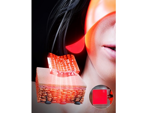 KAIST Team Develops Surface-Lighting MicroLED Patch with Significant Melanogenesis Inhibition Effect
A KAIST research team led by Ph.d candidate Jae Hee Lee and Professor Keon Jae Lee from the Department of Materials Science and Engineering has developed a surface-lighting microLED patch for UV-induced melanogenesis inhibition.
Melanin is brown or dark pigments existing in the skin, which can be abnormally synthesized by external UV or stress. Since the excessive melanin leads to skin diseases such as spots and freckles, proper treatment is required to return normal skin condition.
Recently, LED-based photo-stimulators have been released for skin care, however, their therapeutic effect is still controversial. Since conventional LED stimulators cannot conformally attach to the human skin, distance-induced side effects are caused by light loss and high heat transfer. To achieve effective phototreatment, the LED stimulator needs to be irradiated in contact with the human skin surface, enabling proper and uniform light deliver to the dermis with minimal optical loss.
In this work, the research team fabricated skin-attachable surface-lighting microLED (SµLED, 4 × 4 cm2) patch by utilizing a thousand of microLED chips and silica-embedded light diffusion layer. 100 µm-sized LED chips are vertically-interconnected for high flexibility and low heat generation, allowing its long-term operation on the human skin.
< Image 1. The overall concept of SµLED patch. a) SµLED patch operated on the human skin. b) Schematic illustration of SµLED patch structure. c) 4 × 4 cm2-sized SµLED patch. d) Schematic illustration of the advantages of SµLED patch such as efficient light delivery, low heat generation, and surface-lighting irradiation. >
The research team confirmed melanogenesis inhibition by irradiating the SµLED patch and the conventional LED (CLED) on the artificial human skin and mice dorsal skin. The SµLED-treated groups of human cells and mouse tissues showed minimal epidermal photo-toxicity and consistently effective reduction in synthesized melanin, compared to CLED-treated groups. In addition, significant suppression of proteins/catalysts expression involved in melanin synthesis such as MITF (microphthalmia-associated transcription factor), Melan-A and tyrosinase was verified.
< Image 2. The efficacy of melanogenesis inhibition on 3D human skin cells. a). Different irradiation conditions for a-MSH (major factor to stimulate melanin synthesis) treated cells. b) The ratio of pigmented area to total epidermis area. c) Relative variance of melanin level in 1 cm2-sized skin cells. A low variance means that melanin is evenly distributed, and a high variance means that the melanin is irregularly distributed. d) Optical images after in vitro experiments for 12 days. Scale bar, 1cm. e) Histological analysis of 3D skin, showing the greatest reduction in melanin after SµLED irradiation. Scale bar, 20 µm. >
< Image 3. The efficacy of melanogenesis inhibition on mouse dorsal skin. a) Optical images of mice dorsal skin after photo-treatment for 20 days. b) Histological analysis of mice dorsal skin. Less brown color means less expression of protein/catalysis involved in melanin synthesis. Scale bar, 50 µm. >
Prof. Keon Jae Lee said, “Our inorganic-based SµLED patch has outstanding characteristics in light efficiency, reliability, and durability. The SµLED patch is expected to give a great impact on the cosmetic field by reducing side effects and maximizing phototherapeutic effects.” The core technology of cosmetic SµLED has been transferred to Fronics co., Ltd, founded by Prof. Lee. Fronics is building foundry and equipment for mass production of SµLED masks for whole face cover and plans to release the products in March next year.
This paper entitled “Wearable Surface-Lighting Micro-Light-Emitting Diode Patch for Melanogenesis Inhibition” was published in the November 2022 issue of Advanced Healthcare Materials.
2022.11.22 View 13247
KAIST Team Develops Surface-Lighting MicroLED Patch with Significant Melanogenesis Inhibition Effect
A KAIST research team led by Ph.d candidate Jae Hee Lee and Professor Keon Jae Lee from the Department of Materials Science and Engineering has developed a surface-lighting microLED patch for UV-induced melanogenesis inhibition.
Melanin is brown or dark pigments existing in the skin, which can be abnormally synthesized by external UV or stress. Since the excessive melanin leads to skin diseases such as spots and freckles, proper treatment is required to return normal skin condition.
Recently, LED-based photo-stimulators have been released for skin care, however, their therapeutic effect is still controversial. Since conventional LED stimulators cannot conformally attach to the human skin, distance-induced side effects are caused by light loss and high heat transfer. To achieve effective phototreatment, the LED stimulator needs to be irradiated in contact with the human skin surface, enabling proper and uniform light deliver to the dermis with minimal optical loss.
In this work, the research team fabricated skin-attachable surface-lighting microLED (SµLED, 4 × 4 cm2) patch by utilizing a thousand of microLED chips and silica-embedded light diffusion layer. 100 µm-sized LED chips are vertically-interconnected for high flexibility and low heat generation, allowing its long-term operation on the human skin.
< Image 1. The overall concept of SµLED patch. a) SµLED patch operated on the human skin. b) Schematic illustration of SµLED patch structure. c) 4 × 4 cm2-sized SµLED patch. d) Schematic illustration of the advantages of SµLED patch such as efficient light delivery, low heat generation, and surface-lighting irradiation. >
The research team confirmed melanogenesis inhibition by irradiating the SµLED patch and the conventional LED (CLED) on the artificial human skin and mice dorsal skin. The SµLED-treated groups of human cells and mouse tissues showed minimal epidermal photo-toxicity and consistently effective reduction in synthesized melanin, compared to CLED-treated groups. In addition, significant suppression of proteins/catalysts expression involved in melanin synthesis such as MITF (microphthalmia-associated transcription factor), Melan-A and tyrosinase was verified.
< Image 2. The efficacy of melanogenesis inhibition on 3D human skin cells. a). Different irradiation conditions for a-MSH (major factor to stimulate melanin synthesis) treated cells. b) The ratio of pigmented area to total epidermis area. c) Relative variance of melanin level in 1 cm2-sized skin cells. A low variance means that melanin is evenly distributed, and a high variance means that the melanin is irregularly distributed. d) Optical images after in vitro experiments for 12 days. Scale bar, 1cm. e) Histological analysis of 3D skin, showing the greatest reduction in melanin after SµLED irradiation. Scale bar, 20 µm. >
< Image 3. The efficacy of melanogenesis inhibition on mouse dorsal skin. a) Optical images of mice dorsal skin after photo-treatment for 20 days. b) Histological analysis of mice dorsal skin. Less brown color means less expression of protein/catalysis involved in melanin synthesis. Scale bar, 50 µm. >
Prof. Keon Jae Lee said, “Our inorganic-based SµLED patch has outstanding characteristics in light efficiency, reliability, and durability. The SµLED patch is expected to give a great impact on the cosmetic field by reducing side effects and maximizing phototherapeutic effects.” The core technology of cosmetic SµLED has been transferred to Fronics co., Ltd, founded by Prof. Lee. Fronics is building foundry and equipment for mass production of SµLED masks for whole face cover and plans to release the products in March next year.
This paper entitled “Wearable Surface-Lighting Micro-Light-Emitting Diode Patch for Melanogenesis Inhibition” was published in the November 2022 issue of Advanced Healthcare Materials.
2022.11.22 View 13247 -
 New Nanoparticle Drug Combination For Atherosclerosis
Physicochemical cargo-switching nanoparticles (CSNP) designed by KAIST can help significantly reduce cholesterol and macrophage foam cells in arteries, which are the two main triggers for atherosclerotic plaque and inflammation.
The CSNP-based combination drug delivery therapy was proved to exert cholesterol-lowering, anti-inflammatory, and anti-proliferative functions of two common medications for treating and preventing atherosclerosis that are cyclodextrin and statin. Professor Ji-Ho Park and Dr. Heegon Kim from KAIST’s Department of Bio and Brain Engineering said their study has shown great potential for future applications with reduced side effects.
Atherosclerosis is a chronic inflammatory vascular disease that is characterized by the accumulation of cholesterol and cholesterol-loaded macrophage foam cells in the intima. When this atherosclerotic plaque clogs and narrows the artery walls, they restrict blood flow and cause various cardiovascular conditions such as heart attacks and strokes. Heart attacks and strokes are the world’s first and fifth causes of death respectively.
Oral statin administration has been used in clinics as a standard care for atherosclerosis, which is prescribed to lower blood cholesterol and inhibit its accumulation within the plaque. Although statins can effectively prevent the progression of plaque growth, they have only shown modest efficacy in eliminating the already-established plaque. Therefore, patients are required to take statin drugs for the rest of their lives and will always carry the risk of plaque ruptures that can trigger a blood clot.
To address these issues, Professor Park and Dr. Kim exploited another antiatherogenic agent called cyclodextrin. In their paper published in the Journal of Controlled Release on March 10, Professor Park and Dr. Kim reported that the polymeric formulation of cyclodextrin with a diameter of approximately 10 nanometers(nm) can accumulate within the atherosclerotic plaque 14 times more and effectively reduce the plaque even at lower doses, compared to cyclodextrin in a non-polymer structure.
Moreover, although cyclodextrin is known to have a cytotoxic effect on hair cells in the cochlea, which can lead to hearing loss, cyclodextrin polymers developed by Professor Park’s research group exhibited a varying biodistribution profile and did not have this side effect.
In the follow-up study reported in ACS Nano on April 28, the researchers exploited both cyclodextrin and statin and form the cyclodextrin-statin self-assembly drug complex, based on previous findings that each drug can exert local anti-atherosclerosis effect within the plaque. The complex formation processes were optimized to obtain homogeneous and stable nanoparticles with a diameter of about 100 nm for systematic injection.
The therapeutic synergy of cyclodextrin and statin could reportedly enhance plaque-targeted drug delivery and anti-inflammation. Cyclodextrin led to the regression of cholesterol in the established plaque, and the statins were shown to inhibit the proliferation of macrophage foam cells. The study suggested that combination therapy is required to resolve the complex inflammatory cholesterol-rich microenvironment within the plaque.
Professor Park said, “While nanomedicine has been mainly developed for the treatment of cancers, our studies show that nanomedicine can also play a significant role in treating and preventing atherosclerosis, which causes various cardiovascular diseases that are the leading causes of death worldwide.”
This work was supported by KAIST and the National Research Foundation (NRF) of Korea.
Publications:
1. Heegon Kim, Junhee Han, and Ji-Ho Park. (2020) ‘Cyclodextrin polymer improves atherosclerosis therapy and reduces ototoxicity’ Journal of Controlled Release. Volume 319. Page 77-86. Available online at https://doi.org/10.1016/j.jconrel.2019.12.021
2. Kim, H., et al. (2020) ‘Affinity-Driven Design of Cargo-Switching Nanoparticles to Leverage a Cholesterol-Rich Microenvironment for Atherosclerosis Therapy’ ACS Nano. Available online at https://doi.org/10.1021/acsnano.9b08216
Profile: Ji-Ho Park, Ph.D.
Associate Professor
jihopark@kaist.ac.kr
http://openwetware.org/wiki/Park_Lab
Biomaterials Engineering Laboratory (BEL)
Department of Bio and Brain Engineering (BIOENG)
Korea Advanced Institute of Science and Technology (KAIST)
https://www.kaist.ac.kr
Daejeon 34141, Korea
Profile: Heegon Kim, Ph.D.
Postdoctoral Researcher
heegon@kaist.ac.kr
BEL, BIOENG, KAIST
(END)
2020.06.16 View 15458
New Nanoparticle Drug Combination For Atherosclerosis
Physicochemical cargo-switching nanoparticles (CSNP) designed by KAIST can help significantly reduce cholesterol and macrophage foam cells in arteries, which are the two main triggers for atherosclerotic plaque and inflammation.
The CSNP-based combination drug delivery therapy was proved to exert cholesterol-lowering, anti-inflammatory, and anti-proliferative functions of two common medications for treating and preventing atherosclerosis that are cyclodextrin and statin. Professor Ji-Ho Park and Dr. Heegon Kim from KAIST’s Department of Bio and Brain Engineering said their study has shown great potential for future applications with reduced side effects.
Atherosclerosis is a chronic inflammatory vascular disease that is characterized by the accumulation of cholesterol and cholesterol-loaded macrophage foam cells in the intima. When this atherosclerotic plaque clogs and narrows the artery walls, they restrict blood flow and cause various cardiovascular conditions such as heart attacks and strokes. Heart attacks and strokes are the world’s first and fifth causes of death respectively.
Oral statin administration has been used in clinics as a standard care for atherosclerosis, which is prescribed to lower blood cholesterol and inhibit its accumulation within the plaque. Although statins can effectively prevent the progression of plaque growth, they have only shown modest efficacy in eliminating the already-established plaque. Therefore, patients are required to take statin drugs for the rest of their lives and will always carry the risk of plaque ruptures that can trigger a blood clot.
To address these issues, Professor Park and Dr. Kim exploited another antiatherogenic agent called cyclodextrin. In their paper published in the Journal of Controlled Release on March 10, Professor Park and Dr. Kim reported that the polymeric formulation of cyclodextrin with a diameter of approximately 10 nanometers(nm) can accumulate within the atherosclerotic plaque 14 times more and effectively reduce the plaque even at lower doses, compared to cyclodextrin in a non-polymer structure.
Moreover, although cyclodextrin is known to have a cytotoxic effect on hair cells in the cochlea, which can lead to hearing loss, cyclodextrin polymers developed by Professor Park’s research group exhibited a varying biodistribution profile and did not have this side effect.
In the follow-up study reported in ACS Nano on April 28, the researchers exploited both cyclodextrin and statin and form the cyclodextrin-statin self-assembly drug complex, based on previous findings that each drug can exert local anti-atherosclerosis effect within the plaque. The complex formation processes were optimized to obtain homogeneous and stable nanoparticles with a diameter of about 100 nm for systematic injection.
The therapeutic synergy of cyclodextrin and statin could reportedly enhance plaque-targeted drug delivery and anti-inflammation. Cyclodextrin led to the regression of cholesterol in the established plaque, and the statins were shown to inhibit the proliferation of macrophage foam cells. The study suggested that combination therapy is required to resolve the complex inflammatory cholesterol-rich microenvironment within the plaque.
Professor Park said, “While nanomedicine has been mainly developed for the treatment of cancers, our studies show that nanomedicine can also play a significant role in treating and preventing atherosclerosis, which causes various cardiovascular diseases that are the leading causes of death worldwide.”
This work was supported by KAIST and the National Research Foundation (NRF) of Korea.
Publications:
1. Heegon Kim, Junhee Han, and Ji-Ho Park. (2020) ‘Cyclodextrin polymer improves atherosclerosis therapy and reduces ototoxicity’ Journal of Controlled Release. Volume 319. Page 77-86. Available online at https://doi.org/10.1016/j.jconrel.2019.12.021
2. Kim, H., et al. (2020) ‘Affinity-Driven Design of Cargo-Switching Nanoparticles to Leverage a Cholesterol-Rich Microenvironment for Atherosclerosis Therapy’ ACS Nano. Available online at https://doi.org/10.1021/acsnano.9b08216
Profile: Ji-Ho Park, Ph.D.
Associate Professor
jihopark@kaist.ac.kr
http://openwetware.org/wiki/Park_Lab
Biomaterials Engineering Laboratory (BEL)
Department of Bio and Brain Engineering (BIOENG)
Korea Advanced Institute of Science and Technology (KAIST)
https://www.kaist.ac.kr
Daejeon 34141, Korea
Profile: Heegon Kim, Ph.D.
Postdoctoral Researcher
heegon@kaist.ac.kr
BEL, BIOENG, KAIST
(END)
2020.06.16 View 15458 -
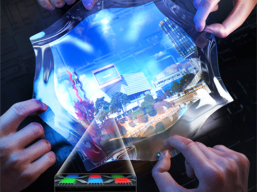 Stress-Relief Substrate Helps OLED Stretch Two-Dimensionally
Highly functional and free-form displays are critical components to complete the technological prowess of wearable electronics, robotics, and human-machine interfaces.
A KAIST team created stretchable OLEDs (Organic Light-Emitting Diodes) that are compliant and maintain their performance under high-strain deformation. Their stress-relief substrates have a unique structure and utilize pillar arrays to reduce the stress on the active areas of devices when strain is applied.
Traditional intrinsically stretchable OLEDs have commercial limitations due to their low efficiency in the electrical conductivity of the electrodes. In addition, previous geometrically stretchable OLEDs laminated to the elastic substrates with thin film devices lead to different pixel emissions of the devices from different peak sizes of the buckles.
To solve these problems, a research team led by Professor Kyung Cheol Choi designed a stretchable substrate system with surface relief island structures that relieve the stress at the locations of bridges in the devices. Their stretchable OLED devices contained an elastic substrate structure comprising bonded elastic pillars and bridges. A patterned upper substrate with bridges makes the rigid substrate stretchable, while the pillars decentralize the stress on the device.
Although various applications using micropillar arrays have been reported, it has not yet been reported how elastic pillar arrays can affect substrates by relieving the stress applied to those substrates upon stretching. Compared to results using similar layouts with conventional free-standing, flat substrates or island structures, their results with elastic pillar arrays show relatively low stress levels at both the bridges and plates when stretching the devices. They achieved stretchable RGB (red, green, blue) OLEDs and had no difficulties with material selection as practical processes were conducted with stress-relief substrates.
Their stretchable OLEDs were mechanically stable and have two-dimensional stretchability, which is superior to only one-direction stretchable electronics, opening the way for practical applications like wearable electronics and health monitoring systems.
Professor Choi said, “Our substrate design will impart flexibility into electronics technology development including semiconductor and circuit technologies. We look forward this new stretchable OLED lowering the barrier for entering the stretchable display market.”
This research was published in Nano Letters titled Two-Dimensionally Stretchable Organic Light-Emitting Diode with Elastic Pillar Arrays for Stress Relief. (https://dx.doi.org/10.1021/acs.nanolett.9b03657). This work was supported by the Engineering Research Center of Excellence Program supported by the National Research Foundation of Korea.
-Profile
Professor Kyung Cheol Choi
kyungcc@kaist.ac.kr
http://adnc.kaist.ac.kr/
School of Electrical Engineering
KAIST
2020.02.27 View 10474
Stress-Relief Substrate Helps OLED Stretch Two-Dimensionally
Highly functional and free-form displays are critical components to complete the technological prowess of wearable electronics, robotics, and human-machine interfaces.
A KAIST team created stretchable OLEDs (Organic Light-Emitting Diodes) that are compliant and maintain their performance under high-strain deformation. Their stress-relief substrates have a unique structure and utilize pillar arrays to reduce the stress on the active areas of devices when strain is applied.
Traditional intrinsically stretchable OLEDs have commercial limitations due to their low efficiency in the electrical conductivity of the electrodes. In addition, previous geometrically stretchable OLEDs laminated to the elastic substrates with thin film devices lead to different pixel emissions of the devices from different peak sizes of the buckles.
To solve these problems, a research team led by Professor Kyung Cheol Choi designed a stretchable substrate system with surface relief island structures that relieve the stress at the locations of bridges in the devices. Their stretchable OLED devices contained an elastic substrate structure comprising bonded elastic pillars and bridges. A patterned upper substrate with bridges makes the rigid substrate stretchable, while the pillars decentralize the stress on the device.
Although various applications using micropillar arrays have been reported, it has not yet been reported how elastic pillar arrays can affect substrates by relieving the stress applied to those substrates upon stretching. Compared to results using similar layouts with conventional free-standing, flat substrates or island structures, their results with elastic pillar arrays show relatively low stress levels at both the bridges and plates when stretching the devices. They achieved stretchable RGB (red, green, blue) OLEDs and had no difficulties with material selection as practical processes were conducted with stress-relief substrates.
Their stretchable OLEDs were mechanically stable and have two-dimensional stretchability, which is superior to only one-direction stretchable electronics, opening the way for practical applications like wearable electronics and health monitoring systems.
Professor Choi said, “Our substrate design will impart flexibility into electronics technology development including semiconductor and circuit technologies. We look forward this new stretchable OLED lowering the barrier for entering the stretchable display market.”
This research was published in Nano Letters titled Two-Dimensionally Stretchable Organic Light-Emitting Diode with Elastic Pillar Arrays for Stress Relief. (https://dx.doi.org/10.1021/acs.nanolett.9b03657). This work was supported by the Engineering Research Center of Excellence Program supported by the National Research Foundation of Korea.
-Profile
Professor Kyung Cheol Choi
kyungcc@kaist.ac.kr
http://adnc.kaist.ac.kr/
School of Electrical Engineering
KAIST
2020.02.27 View 10474