CO
-
 KAIST Identifies Master Regulator Blocking Immunotherapy, Paving the Way for a New Lung Cancer Treatment
Immune checkpoint inhibitors, a class of immunotherapies that help immune cells attack cancer more effectively, have revolutionized cancer treatment. However, fewer than 20% of patients respond to these treatments, highlighting the urgent need for new strategies tailored to both responders and non-responders.
KAIST researchers have discovered that 'DEAD-box helicases 54 (DDX54)', a type of RNA-binding protein, is the master regulator that hinders the effectiveness of immunotherapy—opening a new path for lung cancer treatment. This breakthrough technology has been transferred to faculty startup BioRevert Inc., where it is currently being developed as a companion therapeutic and is expected to enter clinical trials by 2028.
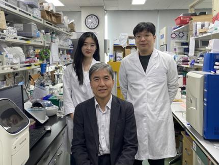
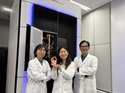
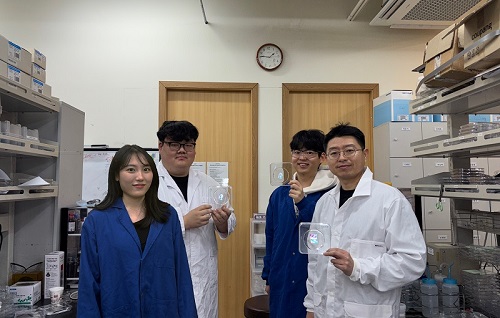
< Photo 1. (From left) Researcher Jungeun Lee, Professor Kwang-Hyun Cho and Postdoctoral Researcher Jeong-Ryeol Gong of the Department of Bio and Brain Engineering at KAIST >
KAIST (represented by President Kwang-Hyung Lee) announced on April 8 that a research team led by Professor Kwang-Hyun Cho from the Department of Bio and Brain Engineering had identified DDX54 as a critical factor that determines the immune evasion capacity of lung cancer cells. They demonstrated that suppressing DDX54 enhances immune cell infiltration into tumors and significantly improves the efficacy of immunotherapy.
Immunotherapy using anti-PD-1 or anti-PD-L1 antibodies is considered a powerful approach in cancer treatment. However, its low response rate limits the number of patients who actually benefit.
To identify likely responders, tumor mutational burden (TMB) has recently been approved by the FDA as a key biomarker for immunotherapy. Cancers with high mutation rates are thought to be more responsive to immune checkpoint inhibitors. However, even tumors with high TMB can display an “immune-desert” phenotype—where immune cell infiltration is severely limited—resulting in poor treatment responses.
< Figure 1. DDX54 was identified as the master regulator that induces resistance to immunotherapy by orchestrating suppression of immune cell infiltration through cancer tissues as lung cancer cells become immune-evasive >
Professor Kwang-Hyun Cho's research team compared transcriptome and genome data of lung cancer patients with immune evasion capabilities through gene regulatory network analysis (A) and discovered DDX54, a master regulator that induces resistance to immunotherapy (B-F).
This study is especially significant in that it successfully demonstrated that suppressing DDX54 in immune-desert lung tumors can overcome immunotherapy resistance and improve treatment outcomes.
The team used transcriptomic and genomic data from immune-evasive lung cancer patients and employed systems biology techniques to infer gene regulatory networks. Through this analysis, they identified DDX54 as a central regulator in the immune evasion of lung cancer cells.
In a syngeneic mouse model, the suppression of DDX54 led to significant increases in the infiltration of anti-cancer immune cells such as T cells and NK cells, and greatly improved the response to immunotherapy.
Single-cell transcriptomic and spatial transcriptomic analyses further showed that combination therapy targeting DDX54 promoted the differentiation of T cells and memory T cells that suppress tumors, while reducing the infiltration of regulatory T cells and exhausted T cells that support tumor growth.
< Figure 2. In the syngeneic mouse model made of lung cancer cells, it was confirmed that inhibiting DDX54 reversed the immune-evasion ability of cancer cells and enhanced the sensitivity to anti-PD-1 therapy >
In a syngeneic mouse model made of lung cancer cells exhibiting immunotherapy resistance, the treatment applied after DDX54 inhibition resulted in statistically significant inhibition of lung cancer growth (B-D) and a significant increase in immune cell infiltration into the tumor tissue (E, F).
The mechanism is believed to involve DDX54 suppression inactivating signaling pathways such as JAK-STAT, MYC, and NF-κB, thereby downregulating immune-evasive proteins CD38 and CD47. This also reduced the infiltration of circulating monocytes—which promote tumor development—and promoted the differentiation of M1 macrophages that play anti-tumor roles.
Professor Kwang-Hyun Cho stated, “We have, for the first time, identified a master regulatory factor that enables immune evasion in lung cancer cells. By targeting this factor, we developed a new therapeutic strategy that can induce responsiveness to immunotherapy in previously resistant cancers.”
He added, “The discovery of DDX54—hidden within the complex molecular networks of cancer cells—was made possible through the systematic integration of systems biology, combining IT and BT.”
The study, led by Professor Kwang-Hyun Cho, was published in the Proceedings of the National Academy of Sciences of the United States of America (PNAS) on April 2, 2025, with Jeong-Ryeol Gong being the first author, Jungeun Lee, a co-first author, and Younghyun Han, a co-author of the article.
< Figure 3. Single-cell transcriptome and spatial transcriptome analysis confirmed that knockdown of DDX54 increased immune cell infiltration into cancer tissues >
In a syngeneic mouse model made of lung cancer cells that underwent immunotherapy in combination with DDX54 inhibition, single-cell transcriptome (H-L) and spatial transcriptome (A-G) analysis of immune cells infiltrating inside cancer tissues were performed. As a result, it was confirmed that anticancer immune cells such as T cells, B cells, and NK cells actively infiltrated the core of lung cancer tissues when DDX54 inhibition and immunotherapy were concurrently administered.
(Paper title: “DDX54 downregulation enhances anti-PD1 therapy in immune-desert lung tumors with high tumor mutational burden,” DOI: https://doi.org/10.1073/pnas.2412310122)
This work was supported by the Ministry of Science and ICT and the National Research Foundation of Korea through the Mid-Career Research Program and Basic Research Laboratory Program.
< Figure 4. The identified master regulator DDX54 was confirmed to induce CD38 and CD47 expression through Jak-Stat3, MYC, and NF-κB activation. >
DDX54 activates the Jak-Stat3, MYC, and NF-κB pathways in lung cancer cells to increase CD38 and CD47 expression (A-G). This creates a cancer microenvironment that contributes to cancer development (H) and ultimately induces immune anticancer treatment resistance.
< Figure 5. It was confirmed that an immune-inflamed environment can be created by combining DDX54 inhibition and immune checkpoint inhibitor (ICI) therapy. >
When DDX54 inhibition and ICI therapy are simultaneously administered, the cancer cell characteristics change, the immune evasion ability is restored, and the environment is transformed into an ‘immune-activated’ environment in which immune cells easily infiltrate cancer tissues. This strengthens the anticancer immune response, thereby increasing the sensitivity of immunotherapy even in lung cancer tissues that previously had low responsiveness to immunotherapy.
2025.04.08 View 5216
KAIST Identifies Master Regulator Blocking Immunotherapy, Paving the Way for a New Lung Cancer Treatment
Immune checkpoint inhibitors, a class of immunotherapies that help immune cells attack cancer more effectively, have revolutionized cancer treatment. However, fewer than 20% of patients respond to these treatments, highlighting the urgent need for new strategies tailored to both responders and non-responders.
KAIST researchers have discovered that 'DEAD-box helicases 54 (DDX54)', a type of RNA-binding protein, is the master regulator that hinders the effectiveness of immunotherapy—opening a new path for lung cancer treatment. This breakthrough technology has been transferred to faculty startup BioRevert Inc., where it is currently being developed as a companion therapeutic and is expected to enter clinical trials by 2028.
< Photo 1. (From left) Researcher Jungeun Lee, Professor Kwang-Hyun Cho and Postdoctoral Researcher Jeong-Ryeol Gong of the Department of Bio and Brain Engineering at KAIST >
KAIST (represented by President Kwang-Hyung Lee) announced on April 8 that a research team led by Professor Kwang-Hyun Cho from the Department of Bio and Brain Engineering had identified DDX54 as a critical factor that determines the immune evasion capacity of lung cancer cells. They demonstrated that suppressing DDX54 enhances immune cell infiltration into tumors and significantly improves the efficacy of immunotherapy.
Immunotherapy using anti-PD-1 or anti-PD-L1 antibodies is considered a powerful approach in cancer treatment. However, its low response rate limits the number of patients who actually benefit.
To identify likely responders, tumor mutational burden (TMB) has recently been approved by the FDA as a key biomarker for immunotherapy. Cancers with high mutation rates are thought to be more responsive to immune checkpoint inhibitors. However, even tumors with high TMB can display an “immune-desert” phenotype—where immune cell infiltration is severely limited—resulting in poor treatment responses.
< Figure 1. DDX54 was identified as the master regulator that induces resistance to immunotherapy by orchestrating suppression of immune cell infiltration through cancer tissues as lung cancer cells become immune-evasive >
Professor Kwang-Hyun Cho's research team compared transcriptome and genome data of lung cancer patients with immune evasion capabilities through gene regulatory network analysis (A) and discovered DDX54, a master regulator that induces resistance to immunotherapy (B-F).
This study is especially significant in that it successfully demonstrated that suppressing DDX54 in immune-desert lung tumors can overcome immunotherapy resistance and improve treatment outcomes.
The team used transcriptomic and genomic data from immune-evasive lung cancer patients and employed systems biology techniques to infer gene regulatory networks. Through this analysis, they identified DDX54 as a central regulator in the immune evasion of lung cancer cells.
In a syngeneic mouse model, the suppression of DDX54 led to significant increases in the infiltration of anti-cancer immune cells such as T cells and NK cells, and greatly improved the response to immunotherapy.
Single-cell transcriptomic and spatial transcriptomic analyses further showed that combination therapy targeting DDX54 promoted the differentiation of T cells and memory T cells that suppress tumors, while reducing the infiltration of regulatory T cells and exhausted T cells that support tumor growth.
< Figure 2. In the syngeneic mouse model made of lung cancer cells, it was confirmed that inhibiting DDX54 reversed the immune-evasion ability of cancer cells and enhanced the sensitivity to anti-PD-1 therapy >
In a syngeneic mouse model made of lung cancer cells exhibiting immunotherapy resistance, the treatment applied after DDX54 inhibition resulted in statistically significant inhibition of lung cancer growth (B-D) and a significant increase in immune cell infiltration into the tumor tissue (E, F).
The mechanism is believed to involve DDX54 suppression inactivating signaling pathways such as JAK-STAT, MYC, and NF-κB, thereby downregulating immune-evasive proteins CD38 and CD47. This also reduced the infiltration of circulating monocytes—which promote tumor development—and promoted the differentiation of M1 macrophages that play anti-tumor roles.
Professor Kwang-Hyun Cho stated, “We have, for the first time, identified a master regulatory factor that enables immune evasion in lung cancer cells. By targeting this factor, we developed a new therapeutic strategy that can induce responsiveness to immunotherapy in previously resistant cancers.”
He added, “The discovery of DDX54—hidden within the complex molecular networks of cancer cells—was made possible through the systematic integration of systems biology, combining IT and BT.”
The study, led by Professor Kwang-Hyun Cho, was published in the Proceedings of the National Academy of Sciences of the United States of America (PNAS) on April 2, 2025, with Jeong-Ryeol Gong being the first author, Jungeun Lee, a co-first author, and Younghyun Han, a co-author of the article.
< Figure 3. Single-cell transcriptome and spatial transcriptome analysis confirmed that knockdown of DDX54 increased immune cell infiltration into cancer tissues >
In a syngeneic mouse model made of lung cancer cells that underwent immunotherapy in combination with DDX54 inhibition, single-cell transcriptome (H-L) and spatial transcriptome (A-G) analysis of immune cells infiltrating inside cancer tissues were performed. As a result, it was confirmed that anticancer immune cells such as T cells, B cells, and NK cells actively infiltrated the core of lung cancer tissues when DDX54 inhibition and immunotherapy were concurrently administered.
(Paper title: “DDX54 downregulation enhances anti-PD1 therapy in immune-desert lung tumors with high tumor mutational burden,” DOI: https://doi.org/10.1073/pnas.2412310122)
This work was supported by the Ministry of Science and ICT and the National Research Foundation of Korea through the Mid-Career Research Program and Basic Research Laboratory Program.
< Figure 4. The identified master regulator DDX54 was confirmed to induce CD38 and CD47 expression through Jak-Stat3, MYC, and NF-κB activation. >
DDX54 activates the Jak-Stat3, MYC, and NF-κB pathways in lung cancer cells to increase CD38 and CD47 expression (A-G). This creates a cancer microenvironment that contributes to cancer development (H) and ultimately induces immune anticancer treatment resistance.
< Figure 5. It was confirmed that an immune-inflamed environment can be created by combining DDX54 inhibition and immune checkpoint inhibitor (ICI) therapy. >
When DDX54 inhibition and ICI therapy are simultaneously administered, the cancer cell characteristics change, the immune evasion ability is restored, and the environment is transformed into an ‘immune-activated’ environment in which immune cells easily infiltrate cancer tissues. This strengthens the anticancer immune response, thereby increasing the sensitivity of immunotherapy even in lung cancer tissues that previously had low responsiveness to immunotherapy.
2025.04.08 View 5216 -
 KAIST Accelerates Synthetic Microbe Design by Discovering Novel Enzymes Using AI
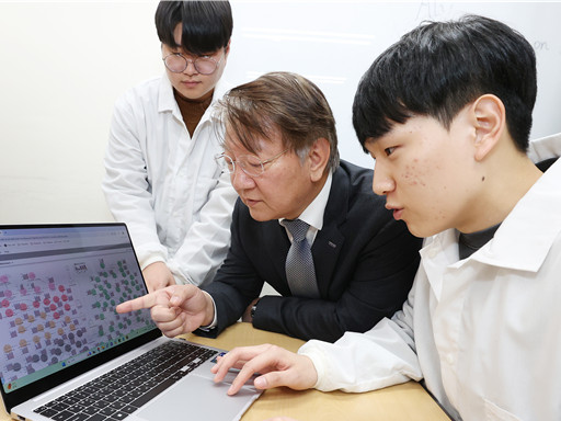
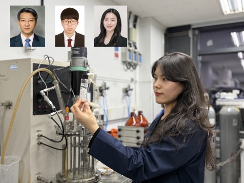
< (From left) Professor Sang Yup Lee of the Department of Chemical and Biomolecular Engineering (top), Hongkeun Ji, PhD candidate of the Department of Chemical and Biomolecular Engineering (top), Ha Rim Kim, PhD candidate of the Department of Chemical and Biomolecular Engineering, and Dr. Gi Bae Kim of the BioProcess Engineering Research Center >
Enzymes are proteins that catalyze biochemical reactions within cells and play a pivotal role in metabolic processes. Accordingly, identifying the functions of novel enzymes is a critical task in the construction of microbial cell factories.
A KAIST research team has leveraged artificial intelligence (AI) to design novel enzymes that do not exist in nature, significantly accelerating microbial cell factory development and boosting the potential for next-generation biotechnological applications such as drug development and biofuel production.
KAIST (represented by President Kwang-Hyung Lee) announced on the 21st of April that Distinguished Professor Sang Yup Lee and his team from the Department of Chemical and Biomolecular Engineering have published a review titled “Enzyme Functional Classification Using Artificial Intelligence,” which outlines the advancement of AI-based enzyme function prediction technologies and analyzes how AI has contributed to the discovery and design of new enzymes.
Professor Lee’s team systematically reviewed the development of enzyme function prediction technologies utilizing machine learning and deep learning, offering a comprehensive analysis.
From sequence similarity-based prediction methods to the integration of convolutional neural networks (CNNs), recurrent neural networks (RNNs), graph neural networks (GNNs), and transformer-based large language models, the paper covers a broad range of AI applications. It analyzes how these technologies extract meaningful information from protein sequences and enhance prediction accuracy.
In particular, enzyme function prediction using deep learning goes beyond simple sequence similarity analysis. By automatically extracting structural and evolutionary features embedded in amino acid sequences, deep learning enables more precise predictions of catalytic functions.
This highlights the unique advantages of AI models compared to traditional bioinformatics approaches.
Moreover, the review suggests that the advancement of generative AI will move future research beyond predicting existing functions to generating entirely new enzymes with functions not found in nature. This shift is expected to profoundly impact the trajectory of biotechnology and synthetic biology.
< Figure 1. Extraction of enzyme characteristics and function prediction using various deep learning structures >
Ha Rim Kim, a Ph.D. candidate and co-first author from the Department of Chemical and Biomolecular Engineering, stated, “AI-based enzyme function prediction and enzyme design are highly important across various fields including metabolic engineering, synthetic biology, and healthcare.”
Distinguished Professor Sang Yup Lee added, “AI-powered enzyme function prediction shows the potential to solve diverse biological problems and will significantly contribute to accelerating research across the entire field.”
The review was published on March 28 in Trends in Biotechnology, a leading biotechnology journal issued by Cell Press.
※ Title: Enzyme Functional Classification Using Artificial Intelligence
※DOI: https://doi.org/10.1016/j.tibtech.2025.03.003
※ Author Information: Ha Rim Kim (KAIST, Co-first author), Hongkeun Ji (KAIST, Co-first author), Gi Bae Kim (KAIST, Third author), Sang Yup Lee (KAIST, Corresponding author)
This research was supported by the Ministry of Science and ICT under the project Development of Core Technologies for Advanced Synthetic Biology to Lead the Bio-Manufacturing Industry (aimed at replacing petroleum-based chemicals), and also by joint support from the Ministry of Science and ICT and the Ministry of Health and Welfare for the project Development of Novel Antibiotic Structures Using Deep Learning-Based Synthetic Biology.
2025.04.07 View 3348
KAIST Accelerates Synthetic Microbe Design by Discovering Novel Enzymes Using AI
< (From left) Professor Sang Yup Lee of the Department of Chemical and Biomolecular Engineering (top), Hongkeun Ji, PhD candidate of the Department of Chemical and Biomolecular Engineering (top), Ha Rim Kim, PhD candidate of the Department of Chemical and Biomolecular Engineering, and Dr. Gi Bae Kim of the BioProcess Engineering Research Center >
Enzymes are proteins that catalyze biochemical reactions within cells and play a pivotal role in metabolic processes. Accordingly, identifying the functions of novel enzymes is a critical task in the construction of microbial cell factories.
A KAIST research team has leveraged artificial intelligence (AI) to design novel enzymes that do not exist in nature, significantly accelerating microbial cell factory development and boosting the potential for next-generation biotechnological applications such as drug development and biofuel production.
KAIST (represented by President Kwang-Hyung Lee) announced on the 21st of April that Distinguished Professor Sang Yup Lee and his team from the Department of Chemical and Biomolecular Engineering have published a review titled “Enzyme Functional Classification Using Artificial Intelligence,” which outlines the advancement of AI-based enzyme function prediction technologies and analyzes how AI has contributed to the discovery and design of new enzymes.
Professor Lee’s team systematically reviewed the development of enzyme function prediction technologies utilizing machine learning and deep learning, offering a comprehensive analysis.
From sequence similarity-based prediction methods to the integration of convolutional neural networks (CNNs), recurrent neural networks (RNNs), graph neural networks (GNNs), and transformer-based large language models, the paper covers a broad range of AI applications. It analyzes how these technologies extract meaningful information from protein sequences and enhance prediction accuracy.
In particular, enzyme function prediction using deep learning goes beyond simple sequence similarity analysis. By automatically extracting structural and evolutionary features embedded in amino acid sequences, deep learning enables more precise predictions of catalytic functions.
This highlights the unique advantages of AI models compared to traditional bioinformatics approaches.
Moreover, the review suggests that the advancement of generative AI will move future research beyond predicting existing functions to generating entirely new enzymes with functions not found in nature. This shift is expected to profoundly impact the trajectory of biotechnology and synthetic biology.
< Figure 1. Extraction of enzyme characteristics and function prediction using various deep learning structures >
Ha Rim Kim, a Ph.D. candidate and co-first author from the Department of Chemical and Biomolecular Engineering, stated, “AI-based enzyme function prediction and enzyme design are highly important across various fields including metabolic engineering, synthetic biology, and healthcare.”
Distinguished Professor Sang Yup Lee added, “AI-powered enzyme function prediction shows the potential to solve diverse biological problems and will significantly contribute to accelerating research across the entire field.”
The review was published on March 28 in Trends in Biotechnology, a leading biotechnology journal issued by Cell Press.
※ Title: Enzyme Functional Classification Using Artificial Intelligence
※DOI: https://doi.org/10.1016/j.tibtech.2025.03.003
※ Author Information: Ha Rim Kim (KAIST, Co-first author), Hongkeun Ji (KAIST, Co-first author), Gi Bae Kim (KAIST, Third author), Sang Yup Lee (KAIST, Corresponding author)
This research was supported by the Ministry of Science and ICT under the project Development of Core Technologies for Advanced Synthetic Biology to Lead the Bio-Manufacturing Industry (aimed at replacing petroleum-based chemicals), and also by joint support from the Ministry of Science and ICT and the Ministry of Health and Welfare for the project Development of Novel Antibiotic Structures Using Deep Learning-Based Synthetic Biology.
2025.04.07 View 3348 -
 KAIST Develops Retinal Therapy to Restore Lost Vision
Vision is one of the most crucial human senses, yet over 300 million people worldwide are at risk of vision loss due to various retinal diseases. While recent advancements in retinal disease treatments have successfully slowed disease progression, no effective therapy has been developed to restore already lost vision—until now. KAIST researchers have successfully developed a novel drug to restore vision.
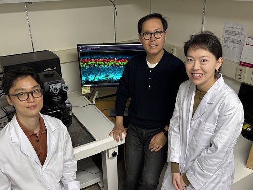
< Photo 1. (From left) Ph.D. candidate Museong Kim, Professor Jin Woo Kim, and Dr. Eun Jung Lee of KAIST Department of Biological Sciences >
KAIST (represented by President Kwang Hyung Lee) announced on the 30th of March that a research team led by Professor Jin Woo Kim from the Department of Biological Sciences has developed a treatment method that restores vision through retinal nerve regeneration.
The research team successfully induced retinal regeneration and vision recovery in a disease-model mouse by administering a compound that blocks the PROX1 (prospero homeobox 1) protein, which suppresses retinal regeneration. Furthermore, the effect lasted for more than six months.
This study marks the first successful induction of long-term neural regeneration in mammalian retinas, offering new hope to patients with degenerative retinal diseases who previously had no treatment options.
As the global population continues to age, the number of retinal disease patients is steadily increasing. However, no treatments exist to restore damaged retinas and vision. The primary reason for this is the mammalian retina's inability to regenerate once damaged.
Studies on cold-blooded animals, such as fish—known for their robust retinal regeneration—have shown that retinal injuries trigger Müller glia cells to dedifferentiate into retinal progenitor cells, which then generate new neurons. However, in mammals, this process is impaired, leading to permanent retinal damage.
< Figure 1. Schematic diagram of the mechanism of retinal regeneration through inhibition of PROX1 migration. PROX1 protein secreted from retinal damaged retinal neurons transfers to Müllerglia and inhibits dedifferentiation into neural progenitor cells and neural regeneration. When PROX1 is captured outside the cells by an antibody against PROX1 and its transfer to Müllerglia is interfered, dedifferentiation of Müllerglia cells and retinal regeneration processes are resumed, restoring visual function. >
Through this study, the research team identified the PROX1 protein as a key inhibitor of Müller glia dedifferentiation in mammals. PROX1 is a protein found in neurons of the retina, hippocampus, and spinal cord, where it suppresses neural stem cell proliferation and promotes differentiation into neurons.
The researchers discovered that PROX1 accumulates in damaged mouse retinal Müller glia, but is absent in the highly regenerative Müller glia of fish. Furthermore, they demonstrated that the PROX1 found in Müller glia is not synthesized internally but rather taken up from surrounding neurons, which fail to degrade and instead secrete the protein.
Based on this finding, the team developed a method to restore Müller glia’s regenerative ability by eliminating extracellular PROX1 before it reaches these cells.
< Figure 2. Retinal regeneration and visual recovery in a retinitis pigmentosa model mouse through Anti-PROX1 gene therapy. After administration of adeno-associated virus expressing PROX1 neutralizing antibodies (AAV2-Anti-PROX1) to the eyes of RP1 retinitis pigmentosa model mice with vision loss, the photoreceptor cell layer of the retina is restored (A) and vision is restored (B). >
This approach involves using an antibody that binds to PROX1, developed by Celliaz Inc., a biotech startup founded by Professor Jin Woo Kim’s research lab. When administered to disease-model mouse retinas, this antibody significantly promoted neural regeneration. Additionally, when delivered, the antibody gene to the retinas of retinitis pigmentosa disease model mice, it enabled sustained retinal regeneration and vision restoration for over six months.
The retinal regeneration-inducing therapy is currently being developed by Celliaz Inc. for application in various degenerative retinal diseases that currently lack effective treatments. The company aims to begin clinical trials by 2028.
This study was co-authored by Dr. Eun Jung Lee of Celliaz Inc. and Museong Kim, a Ph.D. candidate at KAIST, as joint first authors. The findings were published online on March 26 in the international journal Nature Communications. (Paper Title: Restoration of retinal regenerative potential of Müller glia by disrupting intercellular Prox1 transfer | DOI: 10.1038/s41467-025-58290-8)
Dr. Eun Jung Lee stated, "We are about completing the optimization of the PROX1-neutralizing antibody (CLZ001) and move to preclinical studies before administering it to retinal disease patients. Our goal is to provide a solution for patients at risk of blindness who currently lack proper treatment options."
This research was supported by research funds from Korean National Research Foundation (NRF) and the Korea Drug Development Foundation (KDDF).
2025.03.31 View 12908
KAIST Develops Retinal Therapy to Restore Lost Vision
Vision is one of the most crucial human senses, yet over 300 million people worldwide are at risk of vision loss due to various retinal diseases. While recent advancements in retinal disease treatments have successfully slowed disease progression, no effective therapy has been developed to restore already lost vision—until now. KAIST researchers have successfully developed a novel drug to restore vision.
< Photo 1. (From left) Ph.D. candidate Museong Kim, Professor Jin Woo Kim, and Dr. Eun Jung Lee of KAIST Department of Biological Sciences >
KAIST (represented by President Kwang Hyung Lee) announced on the 30th of March that a research team led by Professor Jin Woo Kim from the Department of Biological Sciences has developed a treatment method that restores vision through retinal nerve regeneration.
The research team successfully induced retinal regeneration and vision recovery in a disease-model mouse by administering a compound that blocks the PROX1 (prospero homeobox 1) protein, which suppresses retinal regeneration. Furthermore, the effect lasted for more than six months.
This study marks the first successful induction of long-term neural regeneration in mammalian retinas, offering new hope to patients with degenerative retinal diseases who previously had no treatment options.
As the global population continues to age, the number of retinal disease patients is steadily increasing. However, no treatments exist to restore damaged retinas and vision. The primary reason for this is the mammalian retina's inability to regenerate once damaged.
Studies on cold-blooded animals, such as fish—known for their robust retinal regeneration—have shown that retinal injuries trigger Müller glia cells to dedifferentiate into retinal progenitor cells, which then generate new neurons. However, in mammals, this process is impaired, leading to permanent retinal damage.
< Figure 1. Schematic diagram of the mechanism of retinal regeneration through inhibition of PROX1 migration. PROX1 protein secreted from retinal damaged retinal neurons transfers to Müllerglia and inhibits dedifferentiation into neural progenitor cells and neural regeneration. When PROX1 is captured outside the cells by an antibody against PROX1 and its transfer to Müllerglia is interfered, dedifferentiation of Müllerglia cells and retinal regeneration processes are resumed, restoring visual function. >
Through this study, the research team identified the PROX1 protein as a key inhibitor of Müller glia dedifferentiation in mammals. PROX1 is a protein found in neurons of the retina, hippocampus, and spinal cord, where it suppresses neural stem cell proliferation and promotes differentiation into neurons.
The researchers discovered that PROX1 accumulates in damaged mouse retinal Müller glia, but is absent in the highly regenerative Müller glia of fish. Furthermore, they demonstrated that the PROX1 found in Müller glia is not synthesized internally but rather taken up from surrounding neurons, which fail to degrade and instead secrete the protein.
Based on this finding, the team developed a method to restore Müller glia’s regenerative ability by eliminating extracellular PROX1 before it reaches these cells.
< Figure 2. Retinal regeneration and visual recovery in a retinitis pigmentosa model mouse through Anti-PROX1 gene therapy. After administration of adeno-associated virus expressing PROX1 neutralizing antibodies (AAV2-Anti-PROX1) to the eyes of RP1 retinitis pigmentosa model mice with vision loss, the photoreceptor cell layer of the retina is restored (A) and vision is restored (B). >
This approach involves using an antibody that binds to PROX1, developed by Celliaz Inc., a biotech startup founded by Professor Jin Woo Kim’s research lab. When administered to disease-model mouse retinas, this antibody significantly promoted neural regeneration. Additionally, when delivered, the antibody gene to the retinas of retinitis pigmentosa disease model mice, it enabled sustained retinal regeneration and vision restoration for over six months.
The retinal regeneration-inducing therapy is currently being developed by Celliaz Inc. for application in various degenerative retinal diseases that currently lack effective treatments. The company aims to begin clinical trials by 2028.
This study was co-authored by Dr. Eun Jung Lee of Celliaz Inc. and Museong Kim, a Ph.D. candidate at KAIST, as joint first authors. The findings were published online on March 26 in the international journal Nature Communications. (Paper Title: Restoration of retinal regenerative potential of Müller glia by disrupting intercellular Prox1 transfer | DOI: 10.1038/s41467-025-58290-8)
Dr. Eun Jung Lee stated, "We are about completing the optimization of the PROX1-neutralizing antibody (CLZ001) and move to preclinical studies before administering it to retinal disease patients. Our goal is to provide a solution for patients at risk of blindness who currently lack proper treatment options."
This research was supported by research funds from Korean National Research Foundation (NRF) and the Korea Drug Development Foundation (KDDF).
2025.03.31 View 12908 -
 KAIST provides a comprehensive resource on microbial cell factories for sustainable chemical production
In silico analysis of five industrial microorganisms identifies optimal strains and metabolic engineering strategies for producing 235 valuable chemicals
Climate change and the depletion of fossil fuels have raised the global need for sustainable chemical production. In response to these environmental challenges, microbial cell factories are gaining attention as eco-friendly platforms for producing chemicals using renewable resources, while metabolic engineering technologies to enhance these cell factories are becoming crucial tools for maximizing production efficiency. However, difficulties in selecting suitable microbial strains and optimizing complex metabolic pathways continue to pose significant obstacles to practical industrial applications.
KAIST (President Kwang-Hyung Lee) announced on 27th of March that Distinguished Professor Sang Yup Lee’s research team in the Department of Chemical and Biomolecular Engineering comprehensively evaluated the production capabilities of various industrial microbial cell factories using in silico simulations and, based on these findings, identified the most suitable microbial strains for producing specific chemicals as well as optimal metabolic engineering strategies.
Previously, researchers attempted to determine the best strains and efficient metabolic engineering strategies among numerous microbial candidates through extensive biological experiments and meticulous verification processes. However, this approach required substantial time and costs. Recently, the introduction of genome-scale metabolic models (GEMs), which reconstruct the metabolic networks within an organism based on its entire genome information, has enabled systematic analysis of metabolic fluxes via computer simulations. This development offers a new way to overcome limitations of conventional experimental approaches, revolutionizing both strain selection and metabolic pathway design.
Accordingly, Professor Lee’s team at the Department of Chemical and Biomolecular Engineering, KAIST, evaluated the production capabilities of five representative industrial microorganisms—Escherichia coli, Saccharomyces cerevisiae, Bacillus subtilis, Corynebacterium glutamicum, and Pseudomonas putida—for 235 bio-based chemicals. Using GEMs, the researchers calculated both the maximum theoretical yields and the maximum achievable yields under industrial conditions for each chemical, thereby establishing criteria to identify the most suitable strains for each target compound.
< Figure 1. Outline of the strategy for improving microbial cell factories using a genome-scale metabolic model (GEM) >
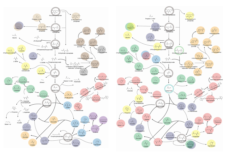
The team specifically proposed strategies such as introducing heterologous enzyme reactions derived from other organisms and exchanging cofactors used by microbes to expand metabolic pathways. These strategies were shown to increase yields beyond the innate metabolic capacities of the microorganisms, resulting in higher production of industrially important chemicals such as mevalonic acid, propanol, fatty acids, and isoprenoids.
Moreover, by applying a computational approach to analyze metabolic fluxes in silico, the researchers suggested strategies for improving microbial strains to maximize the production of various chemicals. They quantitatively identified the relationships between specific enzyme reactions and target chemical production, as well as the relationships between enzymes and metabolites, determining which enzyme reactions should be up- or down-regulated. Through this, the team presented strategies not only to achieve high theoretical yields but also to maximize actual production capacities.
< Figure 2. Comparison of production routes and maximum yields of useful chemicals using representative industrial microorganisms >
Dr. Gi Bae Kim, the first author of this paper from the KAIST BioProcess Engineering Research Center, explained, “By introducing metabolic pathways derived from other organisms and exchanging cofactors, it is possible to design new microbial cell factories that surpass existing limitations. The strategies presented in this study will play a pivotal role in making microbial-based production processes more economical and efficient.” In addition, Distinguished Professor Sang Yup Lee noted, “This research serves as a key resource in the field of systems metabolic engineering, reducing difficulties in strain selection and pathway design, and enabling more efficient development of microbial cell factories. We expect it to greatly contribute to the future development of technologies for producing various eco-friendly chemicals, such as biofuels, bioplastics, and functional food materials.”
This research was conducted with the support from the Development of platform technologies of microbial cell factories for the next-generation biorefineries project and Development of advanced synthetic biology source technologies for leading the biomanufacturing industry project (Project Leader: Distinguished Professor Sang Yup Lee, KAIST) from National Research Foundation supported by the Korean Ministry of Science and ICT.
2025.03.27 View 3809
KAIST provides a comprehensive resource on microbial cell factories for sustainable chemical production
In silico analysis of five industrial microorganisms identifies optimal strains and metabolic engineering strategies for producing 235 valuable chemicals
Climate change and the depletion of fossil fuels have raised the global need for sustainable chemical production. In response to these environmental challenges, microbial cell factories are gaining attention as eco-friendly platforms for producing chemicals using renewable resources, while metabolic engineering technologies to enhance these cell factories are becoming crucial tools for maximizing production efficiency. However, difficulties in selecting suitable microbial strains and optimizing complex metabolic pathways continue to pose significant obstacles to practical industrial applications.
KAIST (President Kwang-Hyung Lee) announced on 27th of March that Distinguished Professor Sang Yup Lee’s research team in the Department of Chemical and Biomolecular Engineering comprehensively evaluated the production capabilities of various industrial microbial cell factories using in silico simulations and, based on these findings, identified the most suitable microbial strains for producing specific chemicals as well as optimal metabolic engineering strategies.
Previously, researchers attempted to determine the best strains and efficient metabolic engineering strategies among numerous microbial candidates through extensive biological experiments and meticulous verification processes. However, this approach required substantial time and costs. Recently, the introduction of genome-scale metabolic models (GEMs), which reconstruct the metabolic networks within an organism based on its entire genome information, has enabled systematic analysis of metabolic fluxes via computer simulations. This development offers a new way to overcome limitations of conventional experimental approaches, revolutionizing both strain selection and metabolic pathway design.
Accordingly, Professor Lee’s team at the Department of Chemical and Biomolecular Engineering, KAIST, evaluated the production capabilities of five representative industrial microorganisms—Escherichia coli, Saccharomyces cerevisiae, Bacillus subtilis, Corynebacterium glutamicum, and Pseudomonas putida—for 235 bio-based chemicals. Using GEMs, the researchers calculated both the maximum theoretical yields and the maximum achievable yields under industrial conditions for each chemical, thereby establishing criteria to identify the most suitable strains for each target compound.
< Figure 1. Outline of the strategy for improving microbial cell factories using a genome-scale metabolic model (GEM) >
The team specifically proposed strategies such as introducing heterologous enzyme reactions derived from other organisms and exchanging cofactors used by microbes to expand metabolic pathways. These strategies were shown to increase yields beyond the innate metabolic capacities of the microorganisms, resulting in higher production of industrially important chemicals such as mevalonic acid, propanol, fatty acids, and isoprenoids.
Moreover, by applying a computational approach to analyze metabolic fluxes in silico, the researchers suggested strategies for improving microbial strains to maximize the production of various chemicals. They quantitatively identified the relationships between specific enzyme reactions and target chemical production, as well as the relationships between enzymes and metabolites, determining which enzyme reactions should be up- or down-regulated. Through this, the team presented strategies not only to achieve high theoretical yields but also to maximize actual production capacities.
< Figure 2. Comparison of production routes and maximum yields of useful chemicals using representative industrial microorganisms >
Dr. Gi Bae Kim, the first author of this paper from the KAIST BioProcess Engineering Research Center, explained, “By introducing metabolic pathways derived from other organisms and exchanging cofactors, it is possible to design new microbial cell factories that surpass existing limitations. The strategies presented in this study will play a pivotal role in making microbial-based production processes more economical and efficient.” In addition, Distinguished Professor Sang Yup Lee noted, “This research serves as a key resource in the field of systems metabolic engineering, reducing difficulties in strain selection and pathway design, and enabling more efficient development of microbial cell factories. We expect it to greatly contribute to the future development of technologies for producing various eco-friendly chemicals, such as biofuels, bioplastics, and functional food materials.”
This research was conducted with the support from the Development of platform technologies of microbial cell factories for the next-generation biorefineries project and Development of advanced synthetic biology source technologies for leading the biomanufacturing industry project (Project Leader: Distinguished Professor Sang Yup Lee, KAIST) from National Research Foundation supported by the Korean Ministry of Science and ICT.
2025.03.27 View 3809 -
 KAIST Captures Protein Reaction in Just Six Milliseconds
Understanding biomolecular processes - such as protein-protein interactions and enzyme-substrate reactions that occur on the microseconds to millisecond time scale is essential for comprehending life processes and advancing drug development. KAIST researchers have developed a method for freezing and analyzing biochemical reaction dynamics within a span of just a few milliseconds, marking a significant step forward in better understanding complex biological reactions.
< Photo. (From left) Professor Jin Young Kang and Haerang Hwang of the Integrated Master's and Doctoral Program of the Department of Chemistry, along with Professor Wonhee Lee of the Department of Physics >
KAIST (represented by President Kwang Hyung Lee) announced on the 24th of March that a joint research team led by Professor Jin Young Kang from the Department of Chemistry and Professor Wonhee Lee from the Department of Physics has developed a parylene-based thin-film microfluidic mixing-and-spraying device for ultra-fast biochemical reaction studies.
*Parylene: A key material for microfluidic devices used to observe protein dynamics at ultra-high speeds. It can be fabricated into a few micrometer-thick films, which can be used in making a spray nozzle for microfluidic devices.
This research overcomes the limitations of the existing time-resolved cryo-electron microscopy (TRCEM) method by reducing sample consumption to one-third of the conventional amount while improving the minimum time resolution—down to just six milliseconds (6 ms).
TRCEM is a technique that rapidly freezes protein complexes during intermediate reaction stages under cryogenic conditions, which allows researchers to analyze their structures. This approach has gained significant attention recently for its ability to capture transient biochemical events.
< Figure 1. Time-resolved cryo-EM (TRCEM) technique using microfluidic channels. In order to capture the intermediate structure of biomolecules during a biochemical reaction over time, biomolecules and reaction substrates are mixed in a microfluidic channel, and then sprayed on a grid after a certain reaction time and frozen in liquid ethane to prepare a cryo-EM sample. This can then be analyzed by cryo-EM to observe the structural changes of proteins over time. >
Transient intermediate structures of protein complexes could not be captured by traditional cryo-electron microscopy due to their extremely short lifespans. Although several TRCEM techniques have been developed to address this issue, previous methods were hindered by large sample consumption and limited time resolution. To overcome these challenges, the KAIST team developed a new mixing-and-spraying device using ultra-thin parylene films. The integrated design of the device further enhanced the precision and reproducibility of experiments.
< Figure 2. TRCEM grid fabrication setup using a parylene-based thin-film microfluidic device and actual appearance of the device. You can see that a thin-film parylene channel is inserted into the injection nozzle. The integration of the reaction channel and the injection nozzle allowed the residence time in the device to be reduced to at least 0.5 ms. >
“This research makes TRCEM more practical and paves the way for diverse applications of the parylene thin-film device in structural biology, drug development, enzyme reaction studies, and biosensor research.” Professor Jin Young Kang explained, emphasizing the significance of the study.
Professor Wonhee Lee added, “The team aims to continue this research, focusing on improvement of the technique to achieve higher time resolution with minimal sample consumption.”
< Figure 3. Comparison of the spraying patterns of the parylene mixing-jet device and the conventional mixing-jet device and the filament length in the resulting RecA-ssDNA filament formation reaction. It was shown that the thin film spray nozzle structure affects the uniformity and accuracy of the final reaction time. >
The research findings, with Haerang Hwang (a graduate student in the integrated master's and Ph.D. program in the Department of Chemistry) as the first author, were published online on January 28, 2025, in the international journal Advanced Functional Materials. (Paper Title: “Integrated Parylene-Based Thin-Film Microfluidic Device for Time-Resolved Cryo-Electron Microscopy”, DOI: doi.org/10.1002/adfm.202418224)
This research was supported by the National Research Foundation of Korea (NRF), the Samsung Future Technology Development Program, and the CELINE consortium.
2025.03.24 View 3661
KAIST Captures Protein Reaction in Just Six Milliseconds
Understanding biomolecular processes - such as protein-protein interactions and enzyme-substrate reactions that occur on the microseconds to millisecond time scale is essential for comprehending life processes and advancing drug development. KAIST researchers have developed a method for freezing and analyzing biochemical reaction dynamics within a span of just a few milliseconds, marking a significant step forward in better understanding complex biological reactions.
< Photo. (From left) Professor Jin Young Kang and Haerang Hwang of the Integrated Master's and Doctoral Program of the Department of Chemistry, along with Professor Wonhee Lee of the Department of Physics >
KAIST (represented by President Kwang Hyung Lee) announced on the 24th of March that a joint research team led by Professor Jin Young Kang from the Department of Chemistry and Professor Wonhee Lee from the Department of Physics has developed a parylene-based thin-film microfluidic mixing-and-spraying device for ultra-fast biochemical reaction studies.
*Parylene: A key material for microfluidic devices used to observe protein dynamics at ultra-high speeds. It can be fabricated into a few micrometer-thick films, which can be used in making a spray nozzle for microfluidic devices.
This research overcomes the limitations of the existing time-resolved cryo-electron microscopy (TRCEM) method by reducing sample consumption to one-third of the conventional amount while improving the minimum time resolution—down to just six milliseconds (6 ms).
TRCEM is a technique that rapidly freezes protein complexes during intermediate reaction stages under cryogenic conditions, which allows researchers to analyze their structures. This approach has gained significant attention recently for its ability to capture transient biochemical events.
< Figure 1. Time-resolved cryo-EM (TRCEM) technique using microfluidic channels. In order to capture the intermediate structure of biomolecules during a biochemical reaction over time, biomolecules and reaction substrates are mixed in a microfluidic channel, and then sprayed on a grid after a certain reaction time and frozen in liquid ethane to prepare a cryo-EM sample. This can then be analyzed by cryo-EM to observe the structural changes of proteins over time. >
Transient intermediate structures of protein complexes could not be captured by traditional cryo-electron microscopy due to their extremely short lifespans. Although several TRCEM techniques have been developed to address this issue, previous methods were hindered by large sample consumption and limited time resolution. To overcome these challenges, the KAIST team developed a new mixing-and-spraying device using ultra-thin parylene films. The integrated design of the device further enhanced the precision and reproducibility of experiments.
< Figure 2. TRCEM grid fabrication setup using a parylene-based thin-film microfluidic device and actual appearance of the device. You can see that a thin-film parylene channel is inserted into the injection nozzle. The integration of the reaction channel and the injection nozzle allowed the residence time in the device to be reduced to at least 0.5 ms. >
“This research makes TRCEM more practical and paves the way for diverse applications of the parylene thin-film device in structural biology, drug development, enzyme reaction studies, and biosensor research.” Professor Jin Young Kang explained, emphasizing the significance of the study.
Professor Wonhee Lee added, “The team aims to continue this research, focusing on improvement of the technique to achieve higher time resolution with minimal sample consumption.”
< Figure 3. Comparison of the spraying patterns of the parylene mixing-jet device and the conventional mixing-jet device and the filament length in the resulting RecA-ssDNA filament formation reaction. It was shown that the thin film spray nozzle structure affects the uniformity and accuracy of the final reaction time. >
The research findings, with Haerang Hwang (a graduate student in the integrated master's and Ph.D. program in the Department of Chemistry) as the first author, were published online on January 28, 2025, in the international journal Advanced Functional Materials. (Paper Title: “Integrated Parylene-Based Thin-Film Microfluidic Device for Time-Resolved Cryo-Electron Microscopy”, DOI: doi.org/10.1002/adfm.202418224)
This research was supported by the National Research Foundation of Korea (NRF), the Samsung Future Technology Development Program, and the CELINE consortium.
2025.03.24 View 3661 -
 KAIST Develops Eco-Friendly, Nylon-Like Plastic Using Microorganisms
Poly(ester amide) amide is a next-generation material that combines the advantages of PET (polyester) and nylon (polyamide), two widely used plastics. However, it could only be produced from fossil fuels, which posed environmental concerns. Using microorganisms, KAIST researchers have successfully developed a new bio-based plastic to replace conventional plastic.
KAIST (represented by President Kwang Hyung Lee) announced on the 20th of March that a research team led by Distinguished Professor Sang Yup Lee from the Department of Chemical and Biomolecular Engineering has developed microbial strains through systems metabolic engineering to produce various eco-friendly, bio-based poly(ester amide)s. The team collaborated with researchers from the Korea Research Institute of Chemical Technology (KRICT, President Young-Kook Lee) to analyze and confirm the properties of the resulting plastic.
Professor Sang Yup Lee’s research team designed new metabolic pathways that do not naturally exist in microorganisms, and developed a platform microbial strain capable of producing nine different types of poly(ester amide)s, including poly(3-hydroxybutyrate-ran-3-aminopropionate) and poly(3-hydroxybutyrate-ran-4-aminobutyrate).
Using glucose derived from abundant biomass sources such as waste wood and weeds, the team successfully produced poly(ester amide)s in an eco-friendly manner. The researchers also confirmed the potential for industrial-scale production by demonstrating high production efficiency (54.57 g/L) using fed-batch fermentation of the engineered strain.
In collaboration with researchers Haemin Jeong and Jihoon Shin from KRICT, the KAIST team analyzed the properties of the bio-based plastic and found that it exhibited characteristics similar to high-density polyethylene (HDPE). This means the new plastic is not only eco-friendly but also strong and durable enough to replace conventional plastics.
The engineered strains and strategies developed in this study are expected to be useful not only for producing various poly(ester amide)s but also for constructing metabolic pathways for the biosynthesis of other types of polymers.
Professor Sang Yup Lee stated, “This study is the first to demonstrate the possibility of producing poly(ester amide)s (plastics) through a renewable bio-based chemical process rather than relying on the petroleum-based chemical industry. We plan to further enhance the production yield and efficiency through continued research.”
The study was published online on March 17 in the international journal Nature Chemical Biology.
·Title: Biosynthesis of poly(ester amide)s in engineered Escherichia coli
·DOI: 10.1038/s41589-025-01842-2
·Authors: A total of seven authors including Tong Un Chae (KAIST, first author), So Young Choi (KAIST, second author), Da-Hee Ahn (KAIST, third author), Woo Dae Jang (KAIST, fourth author), Haemin Jeong (KRICT, fifth author), Jihoon Shin (KRICT, sixth author), and Sang Yup Lee (KAIST, corresponding author).
This research was supported by the Ministry of Science and ICT (MSIT) under the Eco-Friendly Chemical Technology Development Project as part of the "Next-Generation Biorefinery Technology Development to Lead the Bio-Chemical Industry" initiative (project led by Distinguished Professor Sang Yup Lee at KAIST).
2025.03.24 View 5012
KAIST Develops Eco-Friendly, Nylon-Like Plastic Using Microorganisms
Poly(ester amide) amide is a next-generation material that combines the advantages of PET (polyester) and nylon (polyamide), two widely used plastics. However, it could only be produced from fossil fuels, which posed environmental concerns. Using microorganisms, KAIST researchers have successfully developed a new bio-based plastic to replace conventional plastic.
KAIST (represented by President Kwang Hyung Lee) announced on the 20th of March that a research team led by Distinguished Professor Sang Yup Lee from the Department of Chemical and Biomolecular Engineering has developed microbial strains through systems metabolic engineering to produce various eco-friendly, bio-based poly(ester amide)s. The team collaborated with researchers from the Korea Research Institute of Chemical Technology (KRICT, President Young-Kook Lee) to analyze and confirm the properties of the resulting plastic.
Professor Sang Yup Lee’s research team designed new metabolic pathways that do not naturally exist in microorganisms, and developed a platform microbial strain capable of producing nine different types of poly(ester amide)s, including poly(3-hydroxybutyrate-ran-3-aminopropionate) and poly(3-hydroxybutyrate-ran-4-aminobutyrate).
Using glucose derived from abundant biomass sources such as waste wood and weeds, the team successfully produced poly(ester amide)s in an eco-friendly manner. The researchers also confirmed the potential for industrial-scale production by demonstrating high production efficiency (54.57 g/L) using fed-batch fermentation of the engineered strain.
In collaboration with researchers Haemin Jeong and Jihoon Shin from KRICT, the KAIST team analyzed the properties of the bio-based plastic and found that it exhibited characteristics similar to high-density polyethylene (HDPE). This means the new plastic is not only eco-friendly but also strong and durable enough to replace conventional plastics.
The engineered strains and strategies developed in this study are expected to be useful not only for producing various poly(ester amide)s but also for constructing metabolic pathways for the biosynthesis of other types of polymers.
Professor Sang Yup Lee stated, “This study is the first to demonstrate the possibility of producing poly(ester amide)s (plastics) through a renewable bio-based chemical process rather than relying on the petroleum-based chemical industry. We plan to further enhance the production yield and efficiency through continued research.”
The study was published online on March 17 in the international journal Nature Chemical Biology.
·Title: Biosynthesis of poly(ester amide)s in engineered Escherichia coli
·DOI: 10.1038/s41589-025-01842-2
·Authors: A total of seven authors including Tong Un Chae (KAIST, first author), So Young Choi (KAIST, second author), Da-Hee Ahn (KAIST, third author), Woo Dae Jang (KAIST, fourth author), Haemin Jeong (KRICT, fifth author), Jihoon Shin (KRICT, sixth author), and Sang Yup Lee (KAIST, corresponding author).
This research was supported by the Ministry of Science and ICT (MSIT) under the Eco-Friendly Chemical Technology Development Project as part of the "Next-Generation Biorefinery Technology Development to Lead the Bio-Chemical Industry" initiative (project led by Distinguished Professor Sang Yup Lee at KAIST).
2025.03.24 View 5012 -
 No More Touch Issues on Rainy Days! KAIST Develops Human-Like Tactile Sensor
Recent advancements in robotics have enabled machines to handle delicate objects like eggs with precision, thanks to highly integrated pressure sensors that provide detailed tactile feedback. However, even the most advanced robots struggle to accurately detect pressure in complex environments involving water, bending, or electromagnetic interference. A research team at KAIST has successfully developed a pressure sensor that operates stably without external interference, even on wet surfaces like a smartphone screen covered in water, achieving human-level tactile sensitivity.
KAIST (represented by President Kwang Hyung Lee) announced on the 10th of March that a research team led by Professor Jun-Bo Yoon from the School of Electrical Engineering has developed a high-resolution pressure sensor that remains unaffected by external interference such as "ghost touches" caused by moisture on touchscreens.
Capacitive pressure sensors, widely used in touch systems due to their simple structure and durability, are essential components of human-machine interface (HMI) technologies in smartphones, wearable devices, and robots. However, they are prone to malfunctions caused by water droplets, electromagnetic interference, and curves.
To address these issues, the research team investigated the root causes of interference in capacitive pressure sensors. They identified that the "fringe field" generated at the sensor’s edges is particularly susceptible to external disturbances.
The researchers concluded that, to fundamentally resolve this issue, suppressing the fringe field was necessary. Through theoretical analysis, they determined that reducing the electrode spacing to the nanometer scale could effectively minimize the fringe field to below a few percent.
Utilizing proprietary micro/nanofabrication techniques, the team developed a nanogap pressure sensor with an electrode spacing of 900 nanometers (nm). This newly developed sensor reliably detected pressure regardless of the material exerting force and remained unaffected by bending or electromagnetic interference.
Furthermore, the team successfully implemented an artificial tactile system utilizing the developed sensor’s characteristics. Human skin contains specialized pressure receptors called Merkel’s disks. To artificially mimic them, the exclusive detection of pressure was necessary, but hadn’t been achieved by conventional sensors.
Professor Yoon’s research team overcame these challenges, developing a sensor achieving a density comparable to Merkel’s discs and enabling wireless, high-precision pressure sensing.
To explore potential applications, the researcher also developed a force touch pad system, demonstrating its ability to capture pressure magnitude and distribution with high resolution and without interference.
Professor Yoon stated, “Our nanogap pressure sensor operates reliably even in rainy conditions or sweaty environments, eliminating common touch malfunctions. We believe this innovation will significantly enhance everyday user experiences.”
He added, “This technology has the potential to revolutionize various fields, including precision tactile sensors for robotics, medical wearable devices, and next-generation augmented reality (AR) and virtual reality (VR) interfaces.”
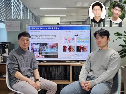
The study was led by Jae-Soon Yang (Ph.D.), Myung-Kun Chung (Ph.D. candidate), and Jae-Young Yoo (Assistant Professor at Sungkyunkwan University, a KAIST Ph.D. graduate). The research findings were published in Nature Communications on February 27, 2025. (Paper title: “Interference-Free Nanogap Pressure Sensor Array with High Spatial Resolution for Wireless Human-Machine Interface Applications”, DOI: 10.1038/s41467-025-57232-8)
This study was supported by the National Research Foundation of Korea’s Mid-Career Researcher Program and Leading Research Center Support Program.
2025.03.14 View 3594
No More Touch Issues on Rainy Days! KAIST Develops Human-Like Tactile Sensor
Recent advancements in robotics have enabled machines to handle delicate objects like eggs with precision, thanks to highly integrated pressure sensors that provide detailed tactile feedback. However, even the most advanced robots struggle to accurately detect pressure in complex environments involving water, bending, or electromagnetic interference. A research team at KAIST has successfully developed a pressure sensor that operates stably without external interference, even on wet surfaces like a smartphone screen covered in water, achieving human-level tactile sensitivity.
KAIST (represented by President Kwang Hyung Lee) announced on the 10th of March that a research team led by Professor Jun-Bo Yoon from the School of Electrical Engineering has developed a high-resolution pressure sensor that remains unaffected by external interference such as "ghost touches" caused by moisture on touchscreens.
Capacitive pressure sensors, widely used in touch systems due to their simple structure and durability, are essential components of human-machine interface (HMI) technologies in smartphones, wearable devices, and robots. However, they are prone to malfunctions caused by water droplets, electromagnetic interference, and curves.
To address these issues, the research team investigated the root causes of interference in capacitive pressure sensors. They identified that the "fringe field" generated at the sensor’s edges is particularly susceptible to external disturbances.
The researchers concluded that, to fundamentally resolve this issue, suppressing the fringe field was necessary. Through theoretical analysis, they determined that reducing the electrode spacing to the nanometer scale could effectively minimize the fringe field to below a few percent.
Utilizing proprietary micro/nanofabrication techniques, the team developed a nanogap pressure sensor with an electrode spacing of 900 nanometers (nm). This newly developed sensor reliably detected pressure regardless of the material exerting force and remained unaffected by bending or electromagnetic interference.
Furthermore, the team successfully implemented an artificial tactile system utilizing the developed sensor’s characteristics. Human skin contains specialized pressure receptors called Merkel’s disks. To artificially mimic them, the exclusive detection of pressure was necessary, but hadn’t been achieved by conventional sensors.
Professor Yoon’s research team overcame these challenges, developing a sensor achieving a density comparable to Merkel’s discs and enabling wireless, high-precision pressure sensing.
To explore potential applications, the researcher also developed a force touch pad system, demonstrating its ability to capture pressure magnitude and distribution with high resolution and without interference.
Professor Yoon stated, “Our nanogap pressure sensor operates reliably even in rainy conditions or sweaty environments, eliminating common touch malfunctions. We believe this innovation will significantly enhance everyday user experiences.”
He added, “This technology has the potential to revolutionize various fields, including precision tactile sensors for robotics, medical wearable devices, and next-generation augmented reality (AR) and virtual reality (VR) interfaces.”
The study was led by Jae-Soon Yang (Ph.D.), Myung-Kun Chung (Ph.D. candidate), and Jae-Young Yoo (Assistant Professor at Sungkyunkwan University, a KAIST Ph.D. graduate). The research findings were published in Nature Communications on February 27, 2025. (Paper title: “Interference-Free Nanogap Pressure Sensor Array with High Spatial Resolution for Wireless Human-Machine Interface Applications”, DOI: 10.1038/s41467-025-57232-8)
This study was supported by the National Research Foundation of Korea’s Mid-Career Researcher Program and Leading Research Center Support Program.
2025.03.14 View 3594 -
 KAIST Develops World-Leading Ammonia Catalyst for Hydrogen Economy
Hydrogen production using renewable energy is a key technology for eco-friendly energy and chemical production. However, storing and transporting hydrogen remains a challenge. To address this, researchers worldwide are investigating methods to store hydrogen in the form of ammonia (NH₃), which is carbon-free and easier to liquify. A research team at KAIST has successfully developed a high-performance catalyst that enables ammonia synthesis at very low temperatures and pressures without energy loss.
KAIST (represented by President Kwang Hyung Lee) announced on the 11th of March that a research team led by Professor Minkee Choi from the Department of Chemical and Biomolecular Engineering has developed an innovative catalytic system that significantly enhances ammonia production while drastically reducing energy consumption and CO₂ emissions.
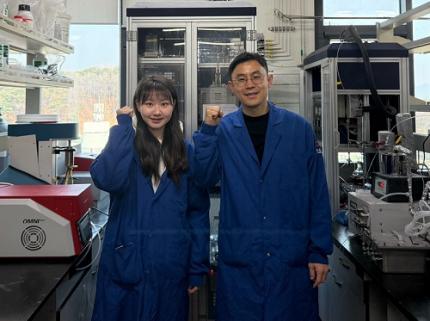
< (From left) Baek Ye-jun, Ph.D. candidate in the Department of Biochemical Engineering, Professor Choi Min-ki >
Currently, ammonia is produced using the Haber-Bosch process, a technology over a century old that relies on iron (Fe)-based catalysts. This method requires extreme conditions—temperatures above 500°C and pressures exceeding 100 atmospheres—resulting in enormous energy consumption and contributing significantly to global CO₂ emissions. Additionally, ammonia is primarily produced in large-scale industrial plants, leading to high distribution costs.
As an alternative, there is growing interest in an eco-friendly process that synthesizes ammonia using green hydrogen—produced via water electrolysis—under mild conditions (300°C, 10 atmospheres). However, developing catalysts that can achieve high ammonia productivity at such low temperatures and pressures is essential, as current technologies struggle to maintain efficiency under these conditions.
The research team developed a novel catalyst by incorporating ruthenium (Ru) nanoparticles and highly basic barium oxide (BaO) particles onto a conductive carbon surface, allowing it to function like a chemical capacitor*.
*Capacitor: A device that stores electrical energy by separating positive and negative charges.
During ammonia synthesis, hydrogen molecules (H₂) first dissociate into hydrogen atoms (H) on the ruthenium catalyst. These hydrogen atoms are further split into protons (H⁺) and electrons (e⁻). The study revealed that the acidic protons are stored in the strongly basic BaO, while the remaining electrons are separated and stored in ruthenium and carbon.
This unique chemical capacitor effect significantly enhances the ruthenium catalyst's electron density, accelerating nitrogen (N₂) dissociation—the rate-limiting step of ammonia synthesis—thereby dramatically increasing catalytic activity.
Furthermore, the team discovered that optimizing the nanostructure of the carbon material further boosts the electron density of ruthenium, maximizing catalytic performance. As a result, the new catalyst demonstrated over seven times higher ammonia synthesis performance compared to state-of-the-art catalysts under mild conditions (300°C, 10 atm).
< Schematic diagram showing the mechanism of ruthenium catalyst activity enhancement by barium oxide cocatalyst >
Professor Minkee Choi stated, “This research has garnered significant attention for demonstrating that catalytic activity can be greatly enhanced by controlling electron transfer within a thermal catalytic reaction system, not just in electrochemical processes.”
He further explained, “Our findings confirm that high-performance catalysts can enable efficient ammonia synthesis under low-temperature and low-pressure conditions. This could shift ammonia production from centralized, large-scale industrial plants to decentralized, small-scale production, making the hydrogen economy more sustainable and flexible.”
The study was led by Professor Minkee Choi as corresponding author and Yaejun Baik, a Ph.D. candidate, as first author. The research findings were published in Nature Catalysis on February 24.
(Paper title: “Electron and proton storage on separate Ru and BaO domains mediated by conductive low-work-function carbon to accelerate ammonia synthesis,” https://doi.org/10.1038/s41929-025-01302-z)
This research was supported by the Korea Institute of Energy Research and the National Research Foundation of Korea.
2025.03.11 View 3113
KAIST Develops World-Leading Ammonia Catalyst for Hydrogen Economy
Hydrogen production using renewable energy is a key technology for eco-friendly energy and chemical production. However, storing and transporting hydrogen remains a challenge. To address this, researchers worldwide are investigating methods to store hydrogen in the form of ammonia (NH₃), which is carbon-free and easier to liquify. A research team at KAIST has successfully developed a high-performance catalyst that enables ammonia synthesis at very low temperatures and pressures without energy loss.
KAIST (represented by President Kwang Hyung Lee) announced on the 11th of March that a research team led by Professor Minkee Choi from the Department of Chemical and Biomolecular Engineering has developed an innovative catalytic system that significantly enhances ammonia production while drastically reducing energy consumption and CO₂ emissions.
< (From left) Baek Ye-jun, Ph.D. candidate in the Department of Biochemical Engineering, Professor Choi Min-ki >
Currently, ammonia is produced using the Haber-Bosch process, a technology over a century old that relies on iron (Fe)-based catalysts. This method requires extreme conditions—temperatures above 500°C and pressures exceeding 100 atmospheres—resulting in enormous energy consumption and contributing significantly to global CO₂ emissions. Additionally, ammonia is primarily produced in large-scale industrial plants, leading to high distribution costs.
As an alternative, there is growing interest in an eco-friendly process that synthesizes ammonia using green hydrogen—produced via water electrolysis—under mild conditions (300°C, 10 atmospheres). However, developing catalysts that can achieve high ammonia productivity at such low temperatures and pressures is essential, as current technologies struggle to maintain efficiency under these conditions.
The research team developed a novel catalyst by incorporating ruthenium (Ru) nanoparticles and highly basic barium oxide (BaO) particles onto a conductive carbon surface, allowing it to function like a chemical capacitor*.
*Capacitor: A device that stores electrical energy by separating positive and negative charges.
During ammonia synthesis, hydrogen molecules (H₂) first dissociate into hydrogen atoms (H) on the ruthenium catalyst. These hydrogen atoms are further split into protons (H⁺) and electrons (e⁻). The study revealed that the acidic protons are stored in the strongly basic BaO, while the remaining electrons are separated and stored in ruthenium and carbon.
This unique chemical capacitor effect significantly enhances the ruthenium catalyst's electron density, accelerating nitrogen (N₂) dissociation—the rate-limiting step of ammonia synthesis—thereby dramatically increasing catalytic activity.
Furthermore, the team discovered that optimizing the nanostructure of the carbon material further boosts the electron density of ruthenium, maximizing catalytic performance. As a result, the new catalyst demonstrated over seven times higher ammonia synthesis performance compared to state-of-the-art catalysts under mild conditions (300°C, 10 atm).
< Schematic diagram showing the mechanism of ruthenium catalyst activity enhancement by barium oxide cocatalyst >
Professor Minkee Choi stated, “This research has garnered significant attention for demonstrating that catalytic activity can be greatly enhanced by controlling electron transfer within a thermal catalytic reaction system, not just in electrochemical processes.”
He further explained, “Our findings confirm that high-performance catalysts can enable efficient ammonia synthesis under low-temperature and low-pressure conditions. This could shift ammonia production from centralized, large-scale industrial plants to decentralized, small-scale production, making the hydrogen economy more sustainable and flexible.”
The study was led by Professor Minkee Choi as corresponding author and Yaejun Baik, a Ph.D. candidate, as first author. The research findings were published in Nature Catalysis on February 24.
(Paper title: “Electron and proton storage on separate Ru and BaO domains mediated by conductive low-work-function carbon to accelerate ammonia synthesis,” https://doi.org/10.1038/s41929-025-01302-z)
This research was supported by the Korea Institute of Energy Research and the National Research Foundation of Korea.
2025.03.11 View 3113 -
 KAIST perfectly reproduces Joseon-era Irworobongdo without pigments
Typically, chemical pigments that absorb specific wavelengths of light within the visible spectrum are required to produce colors. However, KAIST researchers have successfully reproduced the Joseon-era Irworobongdo [일월오봉도] painting using ultra-precise color graphics without any chemical pigments, allowing for the permanent and eco-friendly preservation of color graphics without fading or discoloration.
< (From left) Chaerim Son, a graduate of the Department of Biochemical Engineering (lead author), Seong Kyeong Nam, a graduate of the PhD program, Jiwoo Lee, a PhD student, and Professor Shin-Hyun Kim >
KAIST (represented by President Kwang Hyung Lee) announced on the 26th of February that a research team led by Professor Shinhyun Kim from the Department of Biological and Chemical Engineering had developed a technology that enables high-resolution color graphics without using any chemical pigments by employing hemisphere-shaped microstructures.
Morpho butterflies that are brilliant blue in color or Panther chameleons that change skin color exhibit coloration without chemical pigments, as ordered nanostructures within a material reflect visible light through optical interference. Since structural colors arise from physical structures rather than chemical substances, a single material can produce a wide range of colors.
However, the artificial implementation of structural coloration is highly challenging due to the complexity of creating ordered nanostructures. Additionally, it is difficult to produce a variety of colors and to pattern them precisely into complex designs.
< Figure 1. Principle of structural color expression using micro-hemispheres (left) and method of forming micro-hemisphere patterns based on photolithography (right) >
Professor Kim’s team overcame these challenges by using smooth-surfaced hemispherical microstructures instead of ordered nanostructures, enabling the high-precision patterning of diverse structural colors.
When light enters the inverted hemispherical microstructures, the portion of light entering from the sides undergoes total internal reflection along the curved surface, creating retroreflection. When the hemisphere diameter is approximately 10 micrometers (about one-tenth the thickness of a human hair), light traveling along different reflection paths interferes within the visible spectrum, producing structural coloration.
< Figure 2. “Irworobongdo”, the Painting of the Sun, Moon, and the Five Peaks, reproduced in fingernail size without pigment using approximately 200,000 micro-hemispheres >
The structural color can be tuned by adjusting the size of the hemispheres. By arranging hemispheres of varying sizes, much like mixing paints on a palette, an infinite range of colors can be generated.
To precisely pattern microscale hemispheres of different sizes, the research team employed photolithography* using positive photoresists** commonly used in semiconductor processing. They first patterned photoresists into micropillar structures, then induced reflow*** by heating the material, forming hemispherical microstructures.
*Photolithography: A technique used in semiconductor fabrication to pattern microscale structures.
**Positive photoresist: A photosensitive polymer that dissolves more easily in a developer solution after exposure to ultraviolet light.
***Reflow: A process in which a polymer material softens and reshapes into a curved structure when heated.
This method enables the formation of hemisphere-shaped microstructures with the desired sizes and colors in a single-step fabrication process. It also allows for the reproduction of arbitrary color graphics using a single material without any pigments.
The ultra-precise color graphics created with this technique can exhibit color variations depending on the angle of incident light or the viewing perspective. The pattern appears colored from one direction while remaining transparent from the opposite side, exhibiting a Janus effect. These structural color graphics achieve resolution comparable to cutting-edge LED displays, allowing complex color images to be captured within a fingernail-sized area and projected onto large screens.
< Figure 3. “Irworobongdo” that displays different shades depending on the angle of light and viewing direction >
Professor Shinhyun Kim, who led the research, stated, “Our newly developed pigment-free color graphics technology can serve as an innovative method for artistic expression, merging art with advanced materials. Additionally, it holds broad application potential in optical devices and sensors, anti-counterfeiting materials, aesthetic photocard printing, and many other fields.”
This research, with KAIST researcher Chaerim Son as the first author, was published in the prestigious materials science journal Advanced Materials on February 5.
(Paper title: “Retroreflective Multichrome Microdome Arrays Created by Single-Step Reflow”, DOI: 10.1002/adma.202413143 )
< Figure 4. Famous paintings reproduced without pigment: “Impression, Sunrise” (left), “Girl with a Pearl Earring” (right) >
The study was supported by the National Research Foundation of Korea through the Pioneer Converging Technology R&D Program and the Mid-Career Researcher Program.
2025.02.26 View 4325
KAIST perfectly reproduces Joseon-era Irworobongdo without pigments
Typically, chemical pigments that absorb specific wavelengths of light within the visible spectrum are required to produce colors. However, KAIST researchers have successfully reproduced the Joseon-era Irworobongdo [일월오봉도] painting using ultra-precise color graphics without any chemical pigments, allowing for the permanent and eco-friendly preservation of color graphics without fading or discoloration.
< (From left) Chaerim Son, a graduate of the Department of Biochemical Engineering (lead author), Seong Kyeong Nam, a graduate of the PhD program, Jiwoo Lee, a PhD student, and Professor Shin-Hyun Kim >
KAIST (represented by President Kwang Hyung Lee) announced on the 26th of February that a research team led by Professor Shinhyun Kim from the Department of Biological and Chemical Engineering had developed a technology that enables high-resolution color graphics without using any chemical pigments by employing hemisphere-shaped microstructures.
Morpho butterflies that are brilliant blue in color or Panther chameleons that change skin color exhibit coloration without chemical pigments, as ordered nanostructures within a material reflect visible light through optical interference. Since structural colors arise from physical structures rather than chemical substances, a single material can produce a wide range of colors.
However, the artificial implementation of structural coloration is highly challenging due to the complexity of creating ordered nanostructures. Additionally, it is difficult to produce a variety of colors and to pattern them precisely into complex designs.
< Figure 1. Principle of structural color expression using micro-hemispheres (left) and method of forming micro-hemisphere patterns based on photolithography (right) >
Professor Kim’s team overcame these challenges by using smooth-surfaced hemispherical microstructures instead of ordered nanostructures, enabling the high-precision patterning of diverse structural colors.
When light enters the inverted hemispherical microstructures, the portion of light entering from the sides undergoes total internal reflection along the curved surface, creating retroreflection. When the hemisphere diameter is approximately 10 micrometers (about one-tenth the thickness of a human hair), light traveling along different reflection paths interferes within the visible spectrum, producing structural coloration.
< Figure 2. “Irworobongdo”, the Painting of the Sun, Moon, and the Five Peaks, reproduced in fingernail size without pigment using approximately 200,000 micro-hemispheres >
The structural color can be tuned by adjusting the size of the hemispheres. By arranging hemispheres of varying sizes, much like mixing paints on a palette, an infinite range of colors can be generated.
To precisely pattern microscale hemispheres of different sizes, the research team employed photolithography* using positive photoresists** commonly used in semiconductor processing. They first patterned photoresists into micropillar structures, then induced reflow*** by heating the material, forming hemispherical microstructures.
*Photolithography: A technique used in semiconductor fabrication to pattern microscale structures.
**Positive photoresist: A photosensitive polymer that dissolves more easily in a developer solution after exposure to ultraviolet light.
***Reflow: A process in which a polymer material softens and reshapes into a curved structure when heated.
This method enables the formation of hemisphere-shaped microstructures with the desired sizes and colors in a single-step fabrication process. It also allows for the reproduction of arbitrary color graphics using a single material without any pigments.
The ultra-precise color graphics created with this technique can exhibit color variations depending on the angle of incident light or the viewing perspective. The pattern appears colored from one direction while remaining transparent from the opposite side, exhibiting a Janus effect. These structural color graphics achieve resolution comparable to cutting-edge LED displays, allowing complex color images to be captured within a fingernail-sized area and projected onto large screens.
< Figure 3. “Irworobongdo” that displays different shades depending on the angle of light and viewing direction >
Professor Shinhyun Kim, who led the research, stated, “Our newly developed pigment-free color graphics technology can serve as an innovative method for artistic expression, merging art with advanced materials. Additionally, it holds broad application potential in optical devices and sensors, anti-counterfeiting materials, aesthetic photocard printing, and many other fields.”
This research, with KAIST researcher Chaerim Son as the first author, was published in the prestigious materials science journal Advanced Materials on February 5.
(Paper title: “Retroreflective Multichrome Microdome Arrays Created by Single-Step Reflow”, DOI: 10.1002/adma.202413143 )
< Figure 4. Famous paintings reproduced without pigment: “Impression, Sunrise” (left), “Girl with a Pearl Earring” (right) >
The study was supported by the National Research Foundation of Korea through the Pioneer Converging Technology R&D Program and the Mid-Career Researcher Program.
2025.02.26 View 4325 -
 KAIST achieves quantum entanglement essential for quantum error correction
Quantum computing is a technology capable of solving complex problems that classical computers struggle with. To perform accurate computations, quantum computers must correct errors that arise during operations. However, generating the quantum entanglement necessary for quantum error correction has long been considered a major challenge.
< Photo 1. (From left) Students Young-Do Yoon and Chan Roh of the Master's and Doctoral Integrated Program of the Department of Physics poses with Professor Young-Sik Ra and Student Geunhee Gwak of the same program >
KAIST (represented by President Kwang Hyung Lee) announced on the 25th of February that a research team led by Professor Young-Sik Ra from the Department of Physics has successfully implemented a three-dimensional cluster quantum entangled state, a key component for quantum error correction, through experimental demonstration.
Measurement-based quantum computing is an emerging paradigm that implements quantum computations by measuring specially entangled cluster states. The core of this approach lies in the generation of these cluster quantum entangled states, with two-dimensional cluster states commonly used for universal quantum computing.
However, to advance towards fault-tolerant quantum computing, which can correct quantum errors occurring during computations, a more complex three-dimensional cluster state is required. While previous studies have reported the generation of two-dimensional cluster states, experimental implementation of the three-dimensional cluster states necessary for fault-tolerant quantum computing had remained elusive due to the extreme complexity of their entanglement structure.
< Figure 1. (a) Experimental schematic. A pulse laser with a wavelength of 800 nm is converted into a pulse laser with a wavelength of 400 nm through second harmonic generation, and this is incident on a nonlinear crystal (PPKTP) to generate multiple quantum entanglement sources. (b) Generation of a 3D cluster state through optical mode basis change >
The research team overcame this challenge by developing a technique to control femtosecond time-frequency modes, successfully generating a three-dimensional cluster quantum entangled state for the first time.
The team directed a femtosecond laser into a nonlinear crystal, simultaneously generating quantum light sources across multiple frequency modes. (A femtosecond laser is a device that emits ultrashort, high-intensity light pulses.) Using this approach, they successfully created a three-dimensional cluster quantum entangled state.
Professor Young-Sik Ra noted, “This study marks the first successful demonstration of a three-dimensional cluster quantum entangled state, which was previously difficult to achieve with existing technology. This breakthrough is expected to serve as a crucial stepping stone for future research in measurement-based and fault-tolerant quantum computing.”
< Figure 2. Results of 3D cluster state generation. (a) Nullifier measurement of the cluster state. (b) 3D cluster state reconstructed using quantum state tomography. (c) Confirmation of quantum entanglement characteristics of the 3D cluster state >
The study was published online in Nature Photonics on February 24, 2025. The first author is Chan Roh, a Ph.D. candidate in KAIST’s integrated master’s and doctoral program, with Geunhee Gwak and Youngdo Yoon contributing as co-authors. (Paper title: “Generation of Three-Dimensional Cluster Entangled State”, DOI: 10.1038/s41566-025-01631-2)
This research was supported by the National Research Foundation of Korea (Quantum Computing Technology Development Program, Mid-Career Researcher Support Program, and Quantum Simulator for Materials Innovation Program), the Institute for Information & Communications Technology Planning & Evaluation (Quantum Internet Core Technology Program, University ICT Research Center Support Program), and the U.S. Air Force Research Laboratory.
2025.02.25 View 3298
KAIST achieves quantum entanglement essential for quantum error correction
Quantum computing is a technology capable of solving complex problems that classical computers struggle with. To perform accurate computations, quantum computers must correct errors that arise during operations. However, generating the quantum entanglement necessary for quantum error correction has long been considered a major challenge.
< Photo 1. (From left) Students Young-Do Yoon and Chan Roh of the Master's and Doctoral Integrated Program of the Department of Physics poses with Professor Young-Sik Ra and Student Geunhee Gwak of the same program >
KAIST (represented by President Kwang Hyung Lee) announced on the 25th of February that a research team led by Professor Young-Sik Ra from the Department of Physics has successfully implemented a three-dimensional cluster quantum entangled state, a key component for quantum error correction, through experimental demonstration.
Measurement-based quantum computing is an emerging paradigm that implements quantum computations by measuring specially entangled cluster states. The core of this approach lies in the generation of these cluster quantum entangled states, with two-dimensional cluster states commonly used for universal quantum computing.
However, to advance towards fault-tolerant quantum computing, which can correct quantum errors occurring during computations, a more complex three-dimensional cluster state is required. While previous studies have reported the generation of two-dimensional cluster states, experimental implementation of the three-dimensional cluster states necessary for fault-tolerant quantum computing had remained elusive due to the extreme complexity of their entanglement structure.
< Figure 1. (a) Experimental schematic. A pulse laser with a wavelength of 800 nm is converted into a pulse laser with a wavelength of 400 nm through second harmonic generation, and this is incident on a nonlinear crystal (PPKTP) to generate multiple quantum entanglement sources. (b) Generation of a 3D cluster state through optical mode basis change >
The research team overcame this challenge by developing a technique to control femtosecond time-frequency modes, successfully generating a three-dimensional cluster quantum entangled state for the first time.
The team directed a femtosecond laser into a nonlinear crystal, simultaneously generating quantum light sources across multiple frequency modes. (A femtosecond laser is a device that emits ultrashort, high-intensity light pulses.) Using this approach, they successfully created a three-dimensional cluster quantum entangled state.
Professor Young-Sik Ra noted, “This study marks the first successful demonstration of a three-dimensional cluster quantum entangled state, which was previously difficult to achieve with existing technology. This breakthrough is expected to serve as a crucial stepping stone for future research in measurement-based and fault-tolerant quantum computing.”
< Figure 2. Results of 3D cluster state generation. (a) Nullifier measurement of the cluster state. (b) 3D cluster state reconstructed using quantum state tomography. (c) Confirmation of quantum entanglement characteristics of the 3D cluster state >
The study was published online in Nature Photonics on February 24, 2025. The first author is Chan Roh, a Ph.D. candidate in KAIST’s integrated master’s and doctoral program, with Geunhee Gwak and Youngdo Yoon contributing as co-authors. (Paper title: “Generation of Three-Dimensional Cluster Entangled State”, DOI: 10.1038/s41566-025-01631-2)
This research was supported by the National Research Foundation of Korea (Quantum Computing Technology Development Program, Mid-Career Researcher Support Program, and Quantum Simulator for Materials Innovation Program), the Institute for Information & Communications Technology Planning & Evaluation (Quantum Internet Core Technology Program, University ICT Research Center Support Program), and the U.S. Air Force Research Laboratory.
2025.02.25 View 3298 -
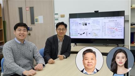 KAIST Research Team Develops an AI Framework Capable of Overcoming the Strength-Ductility Dilemma in Additive-manufactured Titanium Alloys
<(From Left) Ph.D. Student Jaejung Park and Professor Seungchul Lee of KAIST Department of Mechanical Engineering and , Professor Hyoung Seop Kim of POSTECH, and M.S.–Ph.D. Integrated Program Student Jeong Ah Lee of POSTECH. >
The KAIST research team led by Professor Seungchul Lee from Department of Mechanical Engineering, in collaboration with Professor Hyoung Seop Kim’s team at POSTECH, successfully overcame the strength–ductility dilemma of Ti 6Al 4V alloy using artificial intelligence, enabling the production of high strength, high ductility metal products. The AI developed by the team accurately predicts mechanical properties based on various 3D printing process parameters while also providing uncertainty information, and it uses both to recommend process parameters that hold high promise for 3D printing.
Among various 3D printing technologies, laser powder bed fusion is an innovative method for manufacturing Ti-6Al-4V alloy, renowned for its high strength and bio-compatibility. However, this alloy made via 3D printing has traditionally faced challenges in simultaneously achieving high strength and high ductility. Although there have been attempts to address this issue by adjusting both the printing process parameters and heat treatment conditions, the vast number of possible combinations made it difficult to explore them all through experiments and simulations alone.
The active learning framework developed by the team quickly explores a wide range of 3D printing process parameters and heat treatment conditions to recommend those expected to improve both strength and ductility of the alloy. These recommendations are based on the AI model’s predictions of ultimate tensile strength and total elongation along with associated uncertainty information for each set of process parameters and heat treatment conditions. The recommended conditions are then validated by performing 3D printing and tensile tests to obtain the true mechanical property values. These new data are incorporated into further AI model training, and through iterative exploration, the optimal process parameters and heat treatment conditions for producing high-performance alloys were determined in only five iterations. With these optimized conditions, the 3D printed Ti-6Al-4V alloy achieved an ultimate tensile strength of 1190 MPa and a total elongation of 16.5%, successfully overcoming the strength–ductility dilemma.
Professor Seungchul Lee commented, “In this study, by optimizing the 3D printing process parameters and heat treatment conditions, we were able to develop a high-strength, high-ductility Ti-6Al-4V alloy with minimal experimentation trials. Compared to previous studies, we produced an alloy with a similar ultimate tensile strength but higher total elongation, as well as that with a similar elongation but greater ultimate tensile strength.” He added, “Furthermore, if our approach is applied not only to mechanical properties but also to other properties such as thermal conductivity and thermal expansion, we anticipate that it will enable efficient exploration of 3D printing process parameters and heat treatment conditions.”
This study was published in Nature Communications on January 22 (https://doi.org/10.1038/s41467-025-56267-1), and the research was supported by the National Research Foundation of Korea’s Nano & Material Technology Development Program and the Leading Research Center Program.
2025.02.21 View 5213
KAIST Research Team Develops an AI Framework Capable of Overcoming the Strength-Ductility Dilemma in Additive-manufactured Titanium Alloys
<(From Left) Ph.D. Student Jaejung Park and Professor Seungchul Lee of KAIST Department of Mechanical Engineering and , Professor Hyoung Seop Kim of POSTECH, and M.S.–Ph.D. Integrated Program Student Jeong Ah Lee of POSTECH. >
The KAIST research team led by Professor Seungchul Lee from Department of Mechanical Engineering, in collaboration with Professor Hyoung Seop Kim’s team at POSTECH, successfully overcame the strength–ductility dilemma of Ti 6Al 4V alloy using artificial intelligence, enabling the production of high strength, high ductility metal products. The AI developed by the team accurately predicts mechanical properties based on various 3D printing process parameters while also providing uncertainty information, and it uses both to recommend process parameters that hold high promise for 3D printing.
Among various 3D printing technologies, laser powder bed fusion is an innovative method for manufacturing Ti-6Al-4V alloy, renowned for its high strength and bio-compatibility. However, this alloy made via 3D printing has traditionally faced challenges in simultaneously achieving high strength and high ductility. Although there have been attempts to address this issue by adjusting both the printing process parameters and heat treatment conditions, the vast number of possible combinations made it difficult to explore them all through experiments and simulations alone.
The active learning framework developed by the team quickly explores a wide range of 3D printing process parameters and heat treatment conditions to recommend those expected to improve both strength and ductility of the alloy. These recommendations are based on the AI model’s predictions of ultimate tensile strength and total elongation along with associated uncertainty information for each set of process parameters and heat treatment conditions. The recommended conditions are then validated by performing 3D printing and tensile tests to obtain the true mechanical property values. These new data are incorporated into further AI model training, and through iterative exploration, the optimal process parameters and heat treatment conditions for producing high-performance alloys were determined in only five iterations. With these optimized conditions, the 3D printed Ti-6Al-4V alloy achieved an ultimate tensile strength of 1190 MPa and a total elongation of 16.5%, successfully overcoming the strength–ductility dilemma.
Professor Seungchul Lee commented, “In this study, by optimizing the 3D printing process parameters and heat treatment conditions, we were able to develop a high-strength, high-ductility Ti-6Al-4V alloy with minimal experimentation trials. Compared to previous studies, we produced an alloy with a similar ultimate tensile strength but higher total elongation, as well as that with a similar elongation but greater ultimate tensile strength.” He added, “Furthermore, if our approach is applied not only to mechanical properties but also to other properties such as thermal conductivity and thermal expansion, we anticipate that it will enable efficient exploration of 3D printing process parameters and heat treatment conditions.”
This study was published in Nature Communications on January 22 (https://doi.org/10.1038/s41467-025-56267-1), and the research was supported by the National Research Foundation of Korea’s Nano & Material Technology Development Program and the Leading Research Center Program.
2025.02.21 View 5213 -
 KAIST Holds 2025 Commencement Ceremony
KAIST (President Kwang-Hyung Lee) held its 2025 Commencement Ceremony at the Lyu Keun-Chul Sports Complex on the Daejeon Main Campus at 2 p.m. on the 14th of February.
< A scene from KAIST Commencement 2025 - Guests of Honor and Administrative Professors Entering the Stage headed by the color guards of the ELKA (Encouraging Leaders of KAIST) >
At this ceremony, a total of 3,144 degrees were conferred, including 785 doctorates, 1,643 masters, and 716 bachelors. With this, KAIST has produced a total of 81,156 advanced science and technology personnel, including 17,313 doctorates, 41,566 masters, and 22,277 bachelors since its establishment in 1971.
Changyu Lee from the School of Computing received the Minister of Science and ICT Award, and the Chairman of the KAIST Board of Trustees Award went to Lance Khizner Dabu Gragasin, an international student from the Philippines of the Department of Chemical and Biological Engineering. The President’s Award was given to Seoyeong Yang of the Department of Biological Sciences, and the Alumni Association President’s Award and the Development Foundation Chairman’s Award was given to Gahyeon Bae of the Department of Industrial Design and Buyeon Kim of the Department of Mechanical Engineering, respectively.
Minister of Science and ICT Sang-Im Yoo joined the ceremony to deliver a congratulatory speech and to present the awards to outstanding graduates.
< Minister Sang-Im Yoo of the Ministry of Science, Technology and ICT giving his congratulatory message at KAIST Commencement 2025 >
The valedictorian speeches were given by Minjae Kim of the School of Computing, who has practiced the value of sharing that learning is not competition but cooperation, and Mohammed Haruna Hamza of the Department of Aerospace Engineering, a Nigerian international student. Mr. Hamza is the first foreign student to represent the graduating class as valedictorian since the founding of KAIST.
Hamza lost his home and school in his home country due to a terrorist group’s bombing and moved south, but despite the adversity, he continued his studies while pursuing his dream of becoming an aerospace engineer. As a result of his efforts, Hamza was invited by the Korean government to study at KAIST. He expressed his determination to pursue his dream by saying, “I am grateful for the people and experiences that helped me overcome my adversity. The future is the result of the decisions we make today.”
A Pakistani international student was chosen as one of this year's "Most Talked about Graduates of the Year". It is Ali Syed Sheraz who wore his doctoral cap at this year’s commencement ceremony. Ali, a single father who left his one-year-old son behind in his home country, working as a university lecturer. He joined the Ph.D. program in mechanical engineering in 2019 with a passion for mechanical energy.
Ali’s academic journey was full of challenges and growth. Due to COVID-19, his research was suspended for six months, and he had difficulty continuing his studies undergoing three surgeries after a bicycle accident, including a surgery for a fractured elbow, a nose surgery, and removal of kidney stones.
However, he accepted these failure and hardship as a process of growth and participated in the ‘Failed Project Showcase’ and ‘Failure Essay Contest’ held by the KAIST Failure Society, sharing his experiences and growing into a more solid researcher.
< Most Talked about Graduate Graduate of the Year - Syed Sheraz Ali >
Despite experiencing various hardships, he found lessons to learn from them and changed his perspective, which made him unafraid of taking on new challenges. He showed through his own example that failure is not just stumbling blocks but can be a stepping stone to success by looking at his studies and personal life positively.
Furthermore, after becoming the president of the Muslim Student Association, Ali introduced halal menus to the cafeteria on campus so that more Muslim students could eat comfortably. Thanks to this change, his time at KAIST has become an opportunity to understand and experience various cultures more.
Ali is researching artificial muscles (soft actuators) with the world's highest bending strain using MXene, an artificial muscle nanomaterial that can move smoothly, in Professor Il-kwon Oh's lab.
Ali said, "After completing my Ph.D., I plan to develop soft robots, healthcare electronics, and next-generation tactile technology based on MXene, a next-generation 2D material. It is important for my juniors not to be afraid of failure and to have a challenging attitude."
Another 'Most Talked about Graduate of the Year', Mr. Sung-Hyun Jung, who graduated with a master's degree from the Graduate School of Bio Innvation Management, is the CEO of Promedius, a medical AI startup, and has commercialized an osteoporosis diagnosis software based on chest X-rays using AI, and grown it into a leading company in the bone health field.
CEO Jung's challenge shows that KAIST's management education is not just theoretical but practical enough to be applied immediately in the field. CEO Jung, who is also the father of three daughters, experienced business failure in China during the period when the conflict between Korea and China was intensifying.
He moved to Silicon Valley in the United States to revive his business and tried to acquire even small businesses, but the reality was not easy. He worked hard, standing 14 hours a day in a kimchi factory and a restaurant kitchen to make a living. After finishing his life in the United States, CEO Jung returned to Korea and had the opportunity to join Lunit, a global medical AI leader founded by KAIST graduates. CEO Jung experienced the growth of the global medical AI market firsthand with unit Chairman Seungwook Paek.
When he entered the Master's Program at the Graduate School of Bio Innvation Management in 2023 to acquire more specialized knowledge, CEO Jung had just transferred to Promedius and was in a crisis situation with only about 6 months left before the company's funds were exhausted.
While considering a change in business direction because he judged that it would be difficult to survive with existing business items, he learned keywords and investment review perspectives that venture capital (VC) pays attention to in Professor Hoonje Cho’s ‘Bio-innovation Business Startup Strategy and Practice’ class. He attracted 11.4 billion won in investment by applying the investment proposal he wrote based on what he learned from the class to actual practice.
< Most Talked about Graduate of the Year - Sung-Hyun Jung >
In addition, he applied the innovation strategy in the medical field he learned in Professor Kihwan Park’s ‘Innovation and Marketing in Bio and Pharmaceutics’ to the field of osteoporosis, and achieved the result of being selected as the first Asian company to be a corporate advisory committee member of the International Osteoporosis Foundation (IOF). Through this, he established the company as a representative global entity in the osteoporosis field in just one year.
CEO Jung, who applied what he learned from KAIST to actual management and achieved results in the global market in a short period of time, said, “I want to prove that KAIST education is not limited to theory, but is very practical.” He said, “I want to let people know that my life, once full of hardship, got on the track toward success after encountering KAIST,” and expressed his ambition, saying, “My long-term goal is to create a world-class company that is recognized globally.”
In addition, an honorary doctorate was awarded to Chairman Joong Keun Lee of Booyoung Group at the commencement ceremony.
Chairman Joong Keun Lee, who is an entrepreneur that led Booyoung Group, a leading general construction company, received the honorary doctorate in business administration, for leading the development of domestic housing welfare, education, and culture.
KAIST Provost Gyunmin Lee said, “Chairman Joong Keun Lee spared no effort in providing dedicated support for the development of domestic science and technology and the cultivation of future talents. He is awarded the honorary doctorate in recognition of his social responsibility in various fields, including scholarships and support for educational facilities, as well as domestic and international education, culture, veterans affairs, and overseas support.”
Since founding Booyoung Group in 1983, Chairman Lee has boldly entered the rental housing business, a field that large construction companies had avoided, and has played a significant role in improving the quality of life of ordinary citizens by supplying 230,000 households out of 383 complexes and approximately 300,000 households nationwide as rental housing, thereby contributing greatly to the stability of national housing.
< Chairman Joong Keun Lee giving his acceptance speech for his honorary Doctorate >
Chairman Joong Keun Lee, who has been offering hope for a sustainable future, said, “I am honored to receive an honorary doctorate from KAIST, and I hope that KAIST students will nurture their dreams and talents and grow into global talents who will contribute to national development.”
President Kwang-Hyung Lee said, “Chairman Joong Keun Lee has been carrying out various social contribution activities, and in particular, through supporting academic infrastructure, which is the core of national competitiveness, we can see his deep interest in and sense of responsibility for the development of science and technology in our country.” He added, “I am truly delighted to have him as a member of the KAIST family, and I congratulate him on behalf of all members, including our students.”
President Kwang-Hyung Lee also delivered a message of encouragement at the ceremony to charge the graduates to, “Find and keep a dream of your own, be on the lookout for opportunities, don’t be afraid of making mistakes, and do not shy away from taking on challenging tasks.” He added, “Even if you fail, don’t give up. Keep on trying so that you will get to that stage of radiate your own light on the stages where anything is possible.” (End)
2025.02.14 View 6123
KAIST Holds 2025 Commencement Ceremony
KAIST (President Kwang-Hyung Lee) held its 2025 Commencement Ceremony at the Lyu Keun-Chul Sports Complex on the Daejeon Main Campus at 2 p.m. on the 14th of February.
< A scene from KAIST Commencement 2025 - Guests of Honor and Administrative Professors Entering the Stage headed by the color guards of the ELKA (Encouraging Leaders of KAIST) >
At this ceremony, a total of 3,144 degrees were conferred, including 785 doctorates, 1,643 masters, and 716 bachelors. With this, KAIST has produced a total of 81,156 advanced science and technology personnel, including 17,313 doctorates, 41,566 masters, and 22,277 bachelors since its establishment in 1971.
Changyu Lee from the School of Computing received the Minister of Science and ICT Award, and the Chairman of the KAIST Board of Trustees Award went to Lance Khizner Dabu Gragasin, an international student from the Philippines of the Department of Chemical and Biological Engineering. The President’s Award was given to Seoyeong Yang of the Department of Biological Sciences, and the Alumni Association President’s Award and the Development Foundation Chairman’s Award was given to Gahyeon Bae of the Department of Industrial Design and Buyeon Kim of the Department of Mechanical Engineering, respectively.
Minister of Science and ICT Sang-Im Yoo joined the ceremony to deliver a congratulatory speech and to present the awards to outstanding graduates.
< Minister Sang-Im Yoo of the Ministry of Science, Technology and ICT giving his congratulatory message at KAIST Commencement 2025 >
The valedictorian speeches were given by Minjae Kim of the School of Computing, who has practiced the value of sharing that learning is not competition but cooperation, and Mohammed Haruna Hamza of the Department of Aerospace Engineering, a Nigerian international student. Mr. Hamza is the first foreign student to represent the graduating class as valedictorian since the founding of KAIST.
Hamza lost his home and school in his home country due to a terrorist group’s bombing and moved south, but despite the adversity, he continued his studies while pursuing his dream of becoming an aerospace engineer. As a result of his efforts, Hamza was invited by the Korean government to study at KAIST. He expressed his determination to pursue his dream by saying, “I am grateful for the people and experiences that helped me overcome my adversity. The future is the result of the decisions we make today.”
A Pakistani international student was chosen as one of this year's "Most Talked about Graduates of the Year". It is Ali Syed Sheraz who wore his doctoral cap at this year’s commencement ceremony. Ali, a single father who left his one-year-old son behind in his home country, working as a university lecturer. He joined the Ph.D. program in mechanical engineering in 2019 with a passion for mechanical energy.
Ali’s academic journey was full of challenges and growth. Due to COVID-19, his research was suspended for six months, and he had difficulty continuing his studies undergoing three surgeries after a bicycle accident, including a surgery for a fractured elbow, a nose surgery, and removal of kidney stones.
However, he accepted these failure and hardship as a process of growth and participated in the ‘Failed Project Showcase’ and ‘Failure Essay Contest’ held by the KAIST Failure Society, sharing his experiences and growing into a more solid researcher.
< Most Talked about Graduate Graduate of the Year - Syed Sheraz Ali >
Despite experiencing various hardships, he found lessons to learn from them and changed his perspective, which made him unafraid of taking on new challenges. He showed through his own example that failure is not just stumbling blocks but can be a stepping stone to success by looking at his studies and personal life positively.
Furthermore, after becoming the president of the Muslim Student Association, Ali introduced halal menus to the cafeteria on campus so that more Muslim students could eat comfortably. Thanks to this change, his time at KAIST has become an opportunity to understand and experience various cultures more.
Ali is researching artificial muscles (soft actuators) with the world's highest bending strain using MXene, an artificial muscle nanomaterial that can move smoothly, in Professor Il-kwon Oh's lab.
Ali said, "After completing my Ph.D., I plan to develop soft robots, healthcare electronics, and next-generation tactile technology based on MXene, a next-generation 2D material. It is important for my juniors not to be afraid of failure and to have a challenging attitude."
Another 'Most Talked about Graduate of the Year', Mr. Sung-Hyun Jung, who graduated with a master's degree from the Graduate School of Bio Innvation Management, is the CEO of Promedius, a medical AI startup, and has commercialized an osteoporosis diagnosis software based on chest X-rays using AI, and grown it into a leading company in the bone health field.
CEO Jung's challenge shows that KAIST's management education is not just theoretical but practical enough to be applied immediately in the field. CEO Jung, who is also the father of three daughters, experienced business failure in China during the period when the conflict between Korea and China was intensifying.
He moved to Silicon Valley in the United States to revive his business and tried to acquire even small businesses, but the reality was not easy. He worked hard, standing 14 hours a day in a kimchi factory and a restaurant kitchen to make a living. After finishing his life in the United States, CEO Jung returned to Korea and had the opportunity to join Lunit, a global medical AI leader founded by KAIST graduates. CEO Jung experienced the growth of the global medical AI market firsthand with unit Chairman Seungwook Paek.
When he entered the Master's Program at the Graduate School of Bio Innvation Management in 2023 to acquire more specialized knowledge, CEO Jung had just transferred to Promedius and was in a crisis situation with only about 6 months left before the company's funds were exhausted.
While considering a change in business direction because he judged that it would be difficult to survive with existing business items, he learned keywords and investment review perspectives that venture capital (VC) pays attention to in Professor Hoonje Cho’s ‘Bio-innovation Business Startup Strategy and Practice’ class. He attracted 11.4 billion won in investment by applying the investment proposal he wrote based on what he learned from the class to actual practice.
< Most Talked about Graduate of the Year - Sung-Hyun Jung >
In addition, he applied the innovation strategy in the medical field he learned in Professor Kihwan Park’s ‘Innovation and Marketing in Bio and Pharmaceutics’ to the field of osteoporosis, and achieved the result of being selected as the first Asian company to be a corporate advisory committee member of the International Osteoporosis Foundation (IOF). Through this, he established the company as a representative global entity in the osteoporosis field in just one year.
CEO Jung, who applied what he learned from KAIST to actual management and achieved results in the global market in a short period of time, said, “I want to prove that KAIST education is not limited to theory, but is very practical.” He said, “I want to let people know that my life, once full of hardship, got on the track toward success after encountering KAIST,” and expressed his ambition, saying, “My long-term goal is to create a world-class company that is recognized globally.”
In addition, an honorary doctorate was awarded to Chairman Joong Keun Lee of Booyoung Group at the commencement ceremony.
Chairman Joong Keun Lee, who is an entrepreneur that led Booyoung Group, a leading general construction company, received the honorary doctorate in business administration, for leading the development of domestic housing welfare, education, and culture.
KAIST Provost Gyunmin Lee said, “Chairman Joong Keun Lee spared no effort in providing dedicated support for the development of domestic science and technology and the cultivation of future talents. He is awarded the honorary doctorate in recognition of his social responsibility in various fields, including scholarships and support for educational facilities, as well as domestic and international education, culture, veterans affairs, and overseas support.”
Since founding Booyoung Group in 1983, Chairman Lee has boldly entered the rental housing business, a field that large construction companies had avoided, and has played a significant role in improving the quality of life of ordinary citizens by supplying 230,000 households out of 383 complexes and approximately 300,000 households nationwide as rental housing, thereby contributing greatly to the stability of national housing.
< Chairman Joong Keun Lee giving his acceptance speech for his honorary Doctorate >
Chairman Joong Keun Lee, who has been offering hope for a sustainable future, said, “I am honored to receive an honorary doctorate from KAIST, and I hope that KAIST students will nurture their dreams and talents and grow into global talents who will contribute to national development.”
President Kwang-Hyung Lee said, “Chairman Joong Keun Lee has been carrying out various social contribution activities, and in particular, through supporting academic infrastructure, which is the core of national competitiveness, we can see his deep interest in and sense of responsibility for the development of science and technology in our country.” He added, “I am truly delighted to have him as a member of the KAIST family, and I congratulate him on behalf of all members, including our students.”
President Kwang-Hyung Lee also delivered a message of encouragement at the ceremony to charge the graduates to, “Find and keep a dream of your own, be on the lookout for opportunities, don’t be afraid of making mistakes, and do not shy away from taking on challenging tasks.” He added, “Even if you fail, don’t give up. Keep on trying so that you will get to that stage of radiate your own light on the stages where anything is possible.” (End)
2025.02.14 View 6123