CO
-
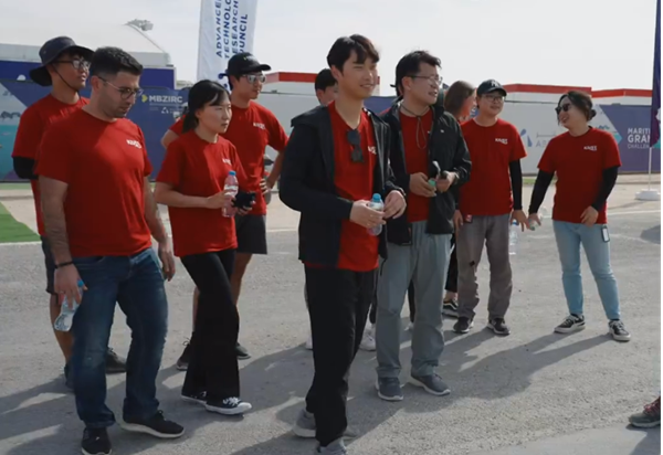 Team KAIST placed among top two at MBZIRC Maritime Grand Challenge
Representing Korean Robotics at Sea: KAIST’s 26-month strife rewarded
Team KAIST placed among top two at MBZIRC Maritime Grand Challenge
- Team KAIST, composed of students from the labs of Professor Jinwhan Kim of the Department of Mechanical Engineering and Professor Hyunchul Shim of the School of Electrical and Engineering, came through the challenge as the first runner-up winning the prize money totaling up to $650,000 (KRW 860 million).
- Successfully led the autonomous collaboration of unmanned aerial and maritime vehicles using cutting-edge robotics and AI technology through to the final round of the competition held in Abu Dhabi from January 10 to February 6, 2024.
KAIST (President Kwang-Hyung Lee), reported on the 8th that Team KAIST, led by students from the labs of Professor Jinwhan Kim of the Department of Mechanical Engineering and Professor Hyunchul Shim of the School of Electrical Engineering, with Pablo Aviation as a partner, won a total prize money of $650,000 (KRW 860 million) at the Maritime Grand Challenge by the Mohamed Bin Zayed International Robotics Challenge (MBZIRC), finishing first runner-up.
This competition, which is the largest ever robotics competition held over water, is sponsored by the government of the United Arab Emirates and organized by ASPIRE, an organization under the Abu Dhabi Ministry of Science, with a total prize money of $3 million.
In the competition, which started at the end of 2021, 52 teams from around the world participated and five teams were selected to go on to the finals in February 2023 after going through the first and second stages of screening. The final round was held from January 10 to February 6, 2024, using actual unmanned ships and drones in a secluded sea area of 10 km2 off the coast of Abu Dhabi, the capital of the United Arab Emirates. A total of 18 KAIST students and Professor Jinwhan Kim and Professor Hyunchul Shim took part in this competition at the location at Abu Dhabi.
Team KAIST will receive $500,000 in prize money for taking second place in the final, and the team’s prize money totals up to $650,000 including $150,000 that was as special midterm award for finalists.
The final mission scenario is to find the target vessel on the run carrying illegal cargoes among many ships moving within the GPS-disabled marine surface, and inspect the deck for two different types of stolen cargo to recover them using the aerial vehicle to bring the small cargo and the robot manipulator topped on an unmanned ship to retrieve the larger one. The true aim of the mission is to complete it through autonomous collaboration of the unmanned ship and the aerial vehicle without human intervention throughout the entire mission process. In particular, since GPS cannot be used in this competition due to regulations, Professor Jinwhan Kim's research team developed autonomous operation techniques for unmanned ships, including searching and navigating methods using maritime radar, and Professor Hyunchul Shim's research team developed video-based navigation and a technology to combine a small autonomous robot with a drone.
The final mission is to retrieve cargo on board a ship fleeing at sea through autonomous collaboration between unmanned ships and unmanned aerial vehicles without human intervention. The overall mission consists the first stage of conducting the inspection to find the target ship among several ships moving at sea and the second stage of conducting the intervention mission to retrieve the cargoes on the deck of the ship. Each team was given a total of three opportunities, and the team that completed the highest-level mission in the shortest time during the three attempts received the highest score.
In the first attempt, KAIST was the only team to succeed in the first stage search mission, but the competition began in earnest as the Croatian team also completed the first stage mission in the second attempt. As the competition schedule was delayed due to strong winds and high waves that continued for several days, the organizers decided to hold the finals with the three teams, including the Team KAIST and the team from Croatia’s the University of Zagreb, which completed the first stage of the mission, and Team Fly-Eagle, a team of researcher from China and UAE that partially completed the first stage. The three teams were given the chance to proceed to the finals and try for the third attempt, and in the final competition, the Croatian team won, KAIST took the second place, and the combined team of UAE-China combined team took the third place. The final prize to be given for the winning team is set at $2 million with $500,000 for the runner-up team, and $250,000 for the third-place.
Professor Jinwhan Kim of the Department of Mechanical Engineering, who served as the advisor for Team KAIST, said, “I would like to express my gratitude and congratulations to the students who put in a huge academic and physical efforts in preparing for the competition over the past two years. I feel rewarded because, regardless of the results, every bit of efforts put into this up to this point will become the base of their confidence and a valuable asset in their growth into a great researcher.” Sol Han, a doctoral student in mechanical engineering who served as the team leader, said, “I am disappointed of how narrowly we missed out on winning at the end, but I am satisfied with the significance of the output we’ve got and I am grateful to the team members who worked hard together for that.”
HD Hyundai, Rainbow Robotics, Avikus, and FIMS also participated as sponsors for Team KAIST's campaign.
2024.02.09 View 3272
Team KAIST placed among top two at MBZIRC Maritime Grand Challenge
Representing Korean Robotics at Sea: KAIST’s 26-month strife rewarded
Team KAIST placed among top two at MBZIRC Maritime Grand Challenge
- Team KAIST, composed of students from the labs of Professor Jinwhan Kim of the Department of Mechanical Engineering and Professor Hyunchul Shim of the School of Electrical and Engineering, came through the challenge as the first runner-up winning the prize money totaling up to $650,000 (KRW 860 million).
- Successfully led the autonomous collaboration of unmanned aerial and maritime vehicles using cutting-edge robotics and AI technology through to the final round of the competition held in Abu Dhabi from January 10 to February 6, 2024.
KAIST (President Kwang-Hyung Lee), reported on the 8th that Team KAIST, led by students from the labs of Professor Jinwhan Kim of the Department of Mechanical Engineering and Professor Hyunchul Shim of the School of Electrical Engineering, with Pablo Aviation as a partner, won a total prize money of $650,000 (KRW 860 million) at the Maritime Grand Challenge by the Mohamed Bin Zayed International Robotics Challenge (MBZIRC), finishing first runner-up.
This competition, which is the largest ever robotics competition held over water, is sponsored by the government of the United Arab Emirates and organized by ASPIRE, an organization under the Abu Dhabi Ministry of Science, with a total prize money of $3 million.
In the competition, which started at the end of 2021, 52 teams from around the world participated and five teams were selected to go on to the finals in February 2023 after going through the first and second stages of screening. The final round was held from January 10 to February 6, 2024, using actual unmanned ships and drones in a secluded sea area of 10 km2 off the coast of Abu Dhabi, the capital of the United Arab Emirates. A total of 18 KAIST students and Professor Jinwhan Kim and Professor Hyunchul Shim took part in this competition at the location at Abu Dhabi.
Team KAIST will receive $500,000 in prize money for taking second place in the final, and the team’s prize money totals up to $650,000 including $150,000 that was as special midterm award for finalists.
The final mission scenario is to find the target vessel on the run carrying illegal cargoes among many ships moving within the GPS-disabled marine surface, and inspect the deck for two different types of stolen cargo to recover them using the aerial vehicle to bring the small cargo and the robot manipulator topped on an unmanned ship to retrieve the larger one. The true aim of the mission is to complete it through autonomous collaboration of the unmanned ship and the aerial vehicle without human intervention throughout the entire mission process. In particular, since GPS cannot be used in this competition due to regulations, Professor Jinwhan Kim's research team developed autonomous operation techniques for unmanned ships, including searching and navigating methods using maritime radar, and Professor Hyunchul Shim's research team developed video-based navigation and a technology to combine a small autonomous robot with a drone.
The final mission is to retrieve cargo on board a ship fleeing at sea through autonomous collaboration between unmanned ships and unmanned aerial vehicles without human intervention. The overall mission consists the first stage of conducting the inspection to find the target ship among several ships moving at sea and the second stage of conducting the intervention mission to retrieve the cargoes on the deck of the ship. Each team was given a total of three opportunities, and the team that completed the highest-level mission in the shortest time during the three attempts received the highest score.
In the first attempt, KAIST was the only team to succeed in the first stage search mission, but the competition began in earnest as the Croatian team also completed the first stage mission in the second attempt. As the competition schedule was delayed due to strong winds and high waves that continued for several days, the organizers decided to hold the finals with the three teams, including the Team KAIST and the team from Croatia’s the University of Zagreb, which completed the first stage of the mission, and Team Fly-Eagle, a team of researcher from China and UAE that partially completed the first stage. The three teams were given the chance to proceed to the finals and try for the third attempt, and in the final competition, the Croatian team won, KAIST took the second place, and the combined team of UAE-China combined team took the third place. The final prize to be given for the winning team is set at $2 million with $500,000 for the runner-up team, and $250,000 for the third-place.
Professor Jinwhan Kim of the Department of Mechanical Engineering, who served as the advisor for Team KAIST, said, “I would like to express my gratitude and congratulations to the students who put in a huge academic and physical efforts in preparing for the competition over the past two years. I feel rewarded because, regardless of the results, every bit of efforts put into this up to this point will become the base of their confidence and a valuable asset in their growth into a great researcher.” Sol Han, a doctoral student in mechanical engineering who served as the team leader, said, “I am disappointed of how narrowly we missed out on winning at the end, but I am satisfied with the significance of the output we’ve got and I am grateful to the team members who worked hard together for that.”
HD Hyundai, Rainbow Robotics, Avikus, and FIMS also participated as sponsors for Team KAIST's campaign.
2024.02.09 View 3272 -
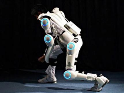 KAIST Research Team Develops Sweat-Resistant Wearable Robot Sensor
New electromyography (EMG) sensor technology that allows the long-term stable control of wearable robots and is not affected by the wearer’s sweat and dead skin has gained attention recently. Wearable robots are devices used across a variety of rehabilitation treatments for the elderly and patients recovering from stroke or trauma.
A joint research team led by Professor Jae-Woong Jung from the KAIST School of Electrical Engineering (EE) and Professor Jung Kim from the KAIST Department of Mechanical Engineering (ME) announced on January 23rd that they have successfully developed a stretchable and adhesive microneedle sensor that can electrically sense physiological signals at a high level without being affected by the state of the user’s skin.
For wearable robots to recognize the intentions behind human movement for their use in rehabilitation treatment, they require a wearable electrophysiological sensor that gives precise EMG measurements. However, existing sensors often show deteriorating signal quality over time and are greatly affected by the user’s skin conditions. Furthermore, the sensor’s higher mechanical hardness causes noise since the contact surface is unable to keep up with the deformation of the skin. These shortcomings limit the reliable, long-term control of wearable robots.
< Figure 1. Design and working concept of the Stretchable microNeedle Adhesive Patch (SNAP). (A) Schematic illustration showing the overall system configuration and application of SNAP. (B) Exploded view schematic diagram of a SNAP, consisting of stretchable serpentine interconnects, Au-coated Si microneedle, and ECA made of Ag flakes–silicone composite. (C) Optical images showing high mechanical compliance of SNAP. >
However, the recently developed technology is expected to allow long-term and high-quality EMG measurements as it uses a stretchable and adhesive conducting substrate integrated with microneedle arrays that can easily penetrate the stratum corneum without causing discomfort. Through its excellent performance, the sensor is anticipated to be able to stably control wearable robots over a long period of time regardless of the wearer’s changing skin conditions and without the need for a preparation step that removes sweat and dead cells from the surface of their skin.
The research team created a stretchable and adhesive microneedle sensor by integrating microneedles into a soft silicon polymer substrate. The hard microneedles penetrate through the stratum corneum, which has high electrical resistance. As a result, the sensor can effectively lower contact resistance with the skin and obtain high-quality electrophysiological signals regardless of contamination. At the same time, the soft and adhesive conducting substrate can adapt to the skin’s surface that stretches with the wearer’s movement, providing a comfortable fit and minimizing noise caused by movement.
< Figure 2. Demonstration of the wireless Stretchable microNeedle Adhesive Patch (SNAP) system as an Human-machine interfaces (HMI) for closed-loop control of an exoskeleton robot. (A) Illustration depicting the system architecture and control strategy of an exoskeleton robot. (B) The hardware configuration of the pneumatic back support exoskeleton system. (C) Comparison of root mean square (RMS) of electromyography (EMG) with and without robotic assistance of pretreated skin and non-pretreated skin. >
To verify the usability of the new patch, the research team conducted a motion assistance experiment using a wearable robot. They attached the microneedle patch on a user’s leg, where it could sense the electrical signals generated by the muscle. The sensor then sent the detected intention to a wearable robot, allowing the robot to help the wearer lift a heavy object more easily.
Professor Jae-Woong Jung, who led the research, said, “The developed stretchable and adhesive microneedle sensor can stability detect EMG signals without being affected by the state of a user’s skin. Through this, we will be able to control wearable robots with higher precision and stability, which will help the rehabilitation of patients who use robots.”
The results of this research, written by co-first authors Heesoo Kim and Juhyun Lee, who are both Ph.D. candidates in the KAIST School of EE, were published in Science Advances on January 17th under the title “Skin-preparation-free, stretchable microneedle adhesive patches for reliable electrophysiological sensing and exoskeleton robot control”.
This research was supported by the Bio-signal Sensor Integrated Technology Development Project by the National Research Foundation of Korea, the Electronic Medicinal Technology Development Project, and the Step 4 BK21 Project.
2024.01.30 View 2477
KAIST Research Team Develops Sweat-Resistant Wearable Robot Sensor
New electromyography (EMG) sensor technology that allows the long-term stable control of wearable robots and is not affected by the wearer’s sweat and dead skin has gained attention recently. Wearable robots are devices used across a variety of rehabilitation treatments for the elderly and patients recovering from stroke or trauma.
A joint research team led by Professor Jae-Woong Jung from the KAIST School of Electrical Engineering (EE) and Professor Jung Kim from the KAIST Department of Mechanical Engineering (ME) announced on January 23rd that they have successfully developed a stretchable and adhesive microneedle sensor that can electrically sense physiological signals at a high level without being affected by the state of the user’s skin.
For wearable robots to recognize the intentions behind human movement for their use in rehabilitation treatment, they require a wearable electrophysiological sensor that gives precise EMG measurements. However, existing sensors often show deteriorating signal quality over time and are greatly affected by the user’s skin conditions. Furthermore, the sensor’s higher mechanical hardness causes noise since the contact surface is unable to keep up with the deformation of the skin. These shortcomings limit the reliable, long-term control of wearable robots.
< Figure 1. Design and working concept of the Stretchable microNeedle Adhesive Patch (SNAP). (A) Schematic illustration showing the overall system configuration and application of SNAP. (B) Exploded view schematic diagram of a SNAP, consisting of stretchable serpentine interconnects, Au-coated Si microneedle, and ECA made of Ag flakes–silicone composite. (C) Optical images showing high mechanical compliance of SNAP. >
However, the recently developed technology is expected to allow long-term and high-quality EMG measurements as it uses a stretchable and adhesive conducting substrate integrated with microneedle arrays that can easily penetrate the stratum corneum without causing discomfort. Through its excellent performance, the sensor is anticipated to be able to stably control wearable robots over a long period of time regardless of the wearer’s changing skin conditions and without the need for a preparation step that removes sweat and dead cells from the surface of their skin.
The research team created a stretchable and adhesive microneedle sensor by integrating microneedles into a soft silicon polymer substrate. The hard microneedles penetrate through the stratum corneum, which has high electrical resistance. As a result, the sensor can effectively lower contact resistance with the skin and obtain high-quality electrophysiological signals regardless of contamination. At the same time, the soft and adhesive conducting substrate can adapt to the skin’s surface that stretches with the wearer’s movement, providing a comfortable fit and minimizing noise caused by movement.
< Figure 2. Demonstration of the wireless Stretchable microNeedle Adhesive Patch (SNAP) system as an Human-machine interfaces (HMI) for closed-loop control of an exoskeleton robot. (A) Illustration depicting the system architecture and control strategy of an exoskeleton robot. (B) The hardware configuration of the pneumatic back support exoskeleton system. (C) Comparison of root mean square (RMS) of electromyography (EMG) with and without robotic assistance of pretreated skin and non-pretreated skin. >
To verify the usability of the new patch, the research team conducted a motion assistance experiment using a wearable robot. They attached the microneedle patch on a user’s leg, where it could sense the electrical signals generated by the muscle. The sensor then sent the detected intention to a wearable robot, allowing the robot to help the wearer lift a heavy object more easily.
Professor Jae-Woong Jung, who led the research, said, “The developed stretchable and adhesive microneedle sensor can stability detect EMG signals without being affected by the state of a user’s skin. Through this, we will be able to control wearable robots with higher precision and stability, which will help the rehabilitation of patients who use robots.”
The results of this research, written by co-first authors Heesoo Kim and Juhyun Lee, who are both Ph.D. candidates in the KAIST School of EE, were published in Science Advances on January 17th under the title “Skin-preparation-free, stretchable microneedle adhesive patches for reliable electrophysiological sensing and exoskeleton robot control”.
This research was supported by the Bio-signal Sensor Integrated Technology Development Project by the National Research Foundation of Korea, the Electronic Medicinal Technology Development Project, and the Step 4 BK21 Project.
2024.01.30 View 2477 -
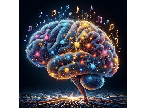 KAIST Research Team Breaks Down Musical Instincts with AI
Music, often referred to as the universal language, is known to be a common component in all cultures. Then, could ‘musical instinct’ be something that is shared to some degree despite the extensive environmental differences amongst cultures?
On January 16, a KAIST research team led by Professor Hawoong Jung from the Department of Physics announced to have identified the principle by which musical instincts emerge from the human brain without special learning using an artificial neural network model.
Previously, many researchers have attempted to identify the similarities and differences between the music that exist in various different cultures, and tried to understand the origin of the universality. A paper published in Science in 2019 had revealed that music is produced in all ethnographically distinct cultures, and that similar forms of beats and tunes are used. Neuroscientist have also previously found out that a specific part of the human brain, namely the auditory cortex, is responsible for processing musical information.
Professor Jung’s team used an artificial neural network model to show that cognitive functions for music forms spontaneously as a result of processing auditory information received from nature, without being taught music. The research team utilized AudioSet, a large-scale collection of sound data provided by Google, and taught the artificial neural network to learn the various sounds. Interestingly, the research team discovered that certain neurons within the network model would respond selectively to music. In other words, they observed the spontaneous generation of neurons that reacted minimally to various other sounds like those of animals, nature, or machines, but showed high levels of response to various forms of music including both instrumental and vocal.
The neurons in the artificial neural network model showed similar reactive behaviours to those in the auditory cortex of a real brain. For example, artificial neurons responded less to the sound of music that was cropped into short intervals and were rearranged. This indicates that the spontaneously-generated music-selective neurons encode the temporal structure of music. This property was not limited to a specific genre of music, but emerged across 25 different genres including classic, pop, rock, jazz, and electronic.
< Figure 1. Illustration of the musicality of the brain and artificial neural network (created with DALL·E3 AI based on the paper content) >
Furthermore, suppressing the activity of the music-selective neurons was found to greatly impede the cognitive accuracy for other natural sounds. That is to say, the neural function that processes musical information helps process other sounds, and that ‘musical ability’ may be an instinct formed as a result of an evolutionary adaptation acquired to better process sounds from nature.
Professor Hawoong Jung, who advised the research, said, “The results of our study imply that evolutionary pressure has contributed to forming the universal basis for processing musical information in various cultures.” As for the significance of the research, he explained, “We look forward for this artificially built model with human-like musicality to become an original model for various applications including AI music generation, musical therapy, and for research in musical cognition.” He also commented on its limitations, adding, “This research however does not take into consideration the developmental process that follows the learning of music, and it must be noted that this is a study on the foundation of processing musical information in early development.”
< Figure 2. The artificial neural network that learned to recognize non-musical natural sounds in the cyber space distinguishes between music and non-music. >
This research, conducted by first author Dr. Gwangsu Kim of the KAIST Department of Physics (current affiliation: MIT Department of Brain and Cognitive Sciences) and Dr. Dong-Kyum Kim (current affiliation: IBS) was published in Nature Communications under the title, “Spontaneous emergence of rudimentary music detectors in deep neural networks”.
This research was supported by the National Research Foundation of Korea.
2024.01.23 View 2142
KAIST Research Team Breaks Down Musical Instincts with AI
Music, often referred to as the universal language, is known to be a common component in all cultures. Then, could ‘musical instinct’ be something that is shared to some degree despite the extensive environmental differences amongst cultures?
On January 16, a KAIST research team led by Professor Hawoong Jung from the Department of Physics announced to have identified the principle by which musical instincts emerge from the human brain without special learning using an artificial neural network model.
Previously, many researchers have attempted to identify the similarities and differences between the music that exist in various different cultures, and tried to understand the origin of the universality. A paper published in Science in 2019 had revealed that music is produced in all ethnographically distinct cultures, and that similar forms of beats and tunes are used. Neuroscientist have also previously found out that a specific part of the human brain, namely the auditory cortex, is responsible for processing musical information.
Professor Jung’s team used an artificial neural network model to show that cognitive functions for music forms spontaneously as a result of processing auditory information received from nature, without being taught music. The research team utilized AudioSet, a large-scale collection of sound data provided by Google, and taught the artificial neural network to learn the various sounds. Interestingly, the research team discovered that certain neurons within the network model would respond selectively to music. In other words, they observed the spontaneous generation of neurons that reacted minimally to various other sounds like those of animals, nature, or machines, but showed high levels of response to various forms of music including both instrumental and vocal.
The neurons in the artificial neural network model showed similar reactive behaviours to those in the auditory cortex of a real brain. For example, artificial neurons responded less to the sound of music that was cropped into short intervals and were rearranged. This indicates that the spontaneously-generated music-selective neurons encode the temporal structure of music. This property was not limited to a specific genre of music, but emerged across 25 different genres including classic, pop, rock, jazz, and electronic.
< Figure 1. Illustration of the musicality of the brain and artificial neural network (created with DALL·E3 AI based on the paper content) >
Furthermore, suppressing the activity of the music-selective neurons was found to greatly impede the cognitive accuracy for other natural sounds. That is to say, the neural function that processes musical information helps process other sounds, and that ‘musical ability’ may be an instinct formed as a result of an evolutionary adaptation acquired to better process sounds from nature.
Professor Hawoong Jung, who advised the research, said, “The results of our study imply that evolutionary pressure has contributed to forming the universal basis for processing musical information in various cultures.” As for the significance of the research, he explained, “We look forward for this artificially built model with human-like musicality to become an original model for various applications including AI music generation, musical therapy, and for research in musical cognition.” He also commented on its limitations, adding, “This research however does not take into consideration the developmental process that follows the learning of music, and it must be noted that this is a study on the foundation of processing musical information in early development.”
< Figure 2. The artificial neural network that learned to recognize non-musical natural sounds in the cyber space distinguishes between music and non-music. >
This research, conducted by first author Dr. Gwangsu Kim of the KAIST Department of Physics (current affiliation: MIT Department of Brain and Cognitive Sciences) and Dr. Dong-Kyum Kim (current affiliation: IBS) was published in Nature Communications under the title, “Spontaneous emergence of rudimentary music detectors in deep neural networks”.
This research was supported by the National Research Foundation of Korea.
2024.01.23 View 2142 -
 KAIST Demonstrates AI and sustainable technologies at CES 2024
On January 2, KAIST announced it will be participating in the Consumer Electronics Show (CES) 2024, held between January 9 and 12.
CES 2024 is one of the world’s largest tech conferences to take place in Las Vegas. Under the slogan “KAIST, the Global Value Creator” for its exhibition, KAIST has submitted technologies falling under one of following themes: “Expansion of Human Intelligence, Mobility, and Reality”, and “Pursuit of Human Security and Sustainable Development”.
24 startups and pre-startups whose technologies stand out in various fields including artificial intelligence (AI), mobility, virtual reality, healthcare and human security, and sustainable development, will welcome their visitors at an exclusive booth of 232 m2 prepared for KAIST at Eureka Park in Las Vegas.
12 businesses will participate in the first category, “Expansion of Human Intelligence, Mobility, and Reality”, including MicroPix, Panmnesia, DeepAuto, MGL, Reports, Narnia Labs, EL FACTORY, Korea Position Technology, AudAi, Planby Technologies, Movin, and Studio Lab.
In the “Pursuit of Human Security and Sustainable Development” category, 12 businesses including Aldaver, ADNC, Solve, Iris, Blue Device, Barreleye, TR, A2US, Greeners, Iron Boys, Shard Partners and Kingbot, will be introduced.
In particular, Aldaver is a startup that received the Korean Business Award 2023 as well as the presidential award at the Challenge K-Startup with its biomimetic material and printing technology. It has attracted 4.5 billion KRW of investment thus far.
Narnia Labs, with its AI design solution for manufacturing, won the grand prize for K-tech Startups 2022, and has so far attracted 3.5 billion KRW of investments.
Panmnesia is a startup that won the 2024 CES Innovation Award, recognized for their fab-less AI semiconductor technology. They attracted 16 billion KRW of investment through seed round alone.
Meanwhile, student startups will also be presented during the exhibition. Studio Lab received a CES 2024 Best of Innovation Award in the AI category. The team developed the software Seller Canvas, which automatically generates a page for product details when a user uploads an image of a product.
The central stage at the KAIST exhibition booth will be used to interview members of the participating startups between Jan 9 to 11, as well as a networking site for businesses and invited investors during KAIST NIGHT on the evening of 10th, between 5 and 7 PM.
Director Sung-Yool Choi of the KAIST Institute of Technology Value Creation said, “Through CES 2024, KAIST will overcome the limits of human intelligence, mobility, and space with the deep-tech based technologies developed by its startups, and will demonstrate its achievements for realizing its vision as a global value-creating university through the solutions for human security and sustainable development.”
2024.01.05 View 3346
KAIST Demonstrates AI and sustainable technologies at CES 2024
On January 2, KAIST announced it will be participating in the Consumer Electronics Show (CES) 2024, held between January 9 and 12.
CES 2024 is one of the world’s largest tech conferences to take place in Las Vegas. Under the slogan “KAIST, the Global Value Creator” for its exhibition, KAIST has submitted technologies falling under one of following themes: “Expansion of Human Intelligence, Mobility, and Reality”, and “Pursuit of Human Security and Sustainable Development”.
24 startups and pre-startups whose technologies stand out in various fields including artificial intelligence (AI), mobility, virtual reality, healthcare and human security, and sustainable development, will welcome their visitors at an exclusive booth of 232 m2 prepared for KAIST at Eureka Park in Las Vegas.
12 businesses will participate in the first category, “Expansion of Human Intelligence, Mobility, and Reality”, including MicroPix, Panmnesia, DeepAuto, MGL, Reports, Narnia Labs, EL FACTORY, Korea Position Technology, AudAi, Planby Technologies, Movin, and Studio Lab.
In the “Pursuit of Human Security and Sustainable Development” category, 12 businesses including Aldaver, ADNC, Solve, Iris, Blue Device, Barreleye, TR, A2US, Greeners, Iron Boys, Shard Partners and Kingbot, will be introduced.
In particular, Aldaver is a startup that received the Korean Business Award 2023 as well as the presidential award at the Challenge K-Startup with its biomimetic material and printing technology. It has attracted 4.5 billion KRW of investment thus far.
Narnia Labs, with its AI design solution for manufacturing, won the grand prize for K-tech Startups 2022, and has so far attracted 3.5 billion KRW of investments.
Panmnesia is a startup that won the 2024 CES Innovation Award, recognized for their fab-less AI semiconductor technology. They attracted 16 billion KRW of investment through seed round alone.
Meanwhile, student startups will also be presented during the exhibition. Studio Lab received a CES 2024 Best of Innovation Award in the AI category. The team developed the software Seller Canvas, which automatically generates a page for product details when a user uploads an image of a product.
The central stage at the KAIST exhibition booth will be used to interview members of the participating startups between Jan 9 to 11, as well as a networking site for businesses and invited investors during KAIST NIGHT on the evening of 10th, between 5 and 7 PM.
Director Sung-Yool Choi of the KAIST Institute of Technology Value Creation said, “Through CES 2024, KAIST will overcome the limits of human intelligence, mobility, and space with the deep-tech based technologies developed by its startups, and will demonstrate its achievements for realizing its vision as a global value-creating university through the solutions for human security and sustainable development.”
2024.01.05 View 3346 -
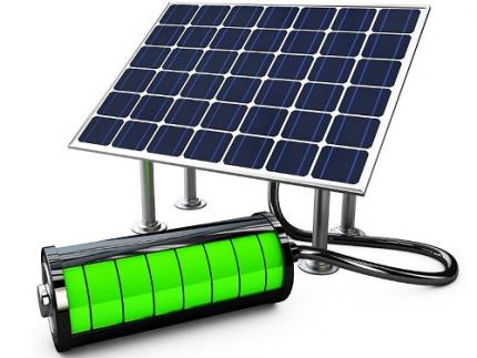 A KAIST Research Team Develops High-Performance Stretchable Solar Cells
With the market for wearable electric devices growing rapidly, stretchable solar cells that can function under strain have received considerable attention as an energy source. To build such solar cells, it is necessary that their photoactive layer, which converts light into electricity, shows high electrical performance while possessing mechanical elasticity. However, satisfying both of these two requirements is challenging, making stretchable solar cells difficult to develop.
On December 26, a KAIST research team from the Department of Chemical and Biomolecular Engineering (CBE) led by Professor Bumjoon Kim announced the development of a new conductive polymer material that achieved both high electrical performance and elasticity while introducing the world’s highest-performing stretchable organic solar cell.
Organic solar cells are devices whose photoactive layer, which is responsible for the conversion of light into electricity, is composed of organic materials. Compared to existing non-organic material-based solar cells, they are lighter and flexible, making them highly applicable for wearable electrical devices. Solar cells as an energy source are particularly important for building electrical devices, but high-efficiency solar cells often lack flexibility, and their application in wearable devices have therefore been limited to this point.
The team led by Professor Kim conjugated a highly stretchable polymer to an electrically conductive polymer with excellent electrical properties through chemical bonding, and developed a new conductive polymer with both electrical conductivity and mechanical stretchability. This polymer meets the highest reported level of photovoltaic conversion efficiency (19%) using organic solar cells, while also showing 10 times the stretchability of existing devices. The team thereby built the world’s highest performing stretchable solar cell that can be stretched up to 40% during operation, and demonstrated its applicability for wearable devices.
< Figure 1. Chemical structure of the newly developed conductive polymer and performance of stretchable organic solar cells using the material. >
Professor Kim said, “Through this research, we not only developed the world’s best performing stretchable organic solar cell, but it is also significant that we developed a new polymer that can be applicable as a base material for various electronic devices that needs to be malleable and/or elastic.”
< Figure 2. Photovoltaic efficiency and mechanical stretchability of newly developed polymers compared to existing polymers. >
This research, conducted by KAIST researchers Jin-Woo Lee and Heung-Goo Lee as first co-authors in cooperation with teams led by Professor Taek-Soo Kim from the Department of Mechanical Engineering and Professor Sheng Li from the Department of CBE, was published in Joule on December 1 (Paper Title: Rigid and Soft Block-Copolymerized Conjugated Polymers Enable High-Performance Intrinsically-Stretchable Organic Solar Cells).
This research was supported by the National Research Foundation of Korea.
2024.01.04 View 3457
A KAIST Research Team Develops High-Performance Stretchable Solar Cells
With the market for wearable electric devices growing rapidly, stretchable solar cells that can function under strain have received considerable attention as an energy source. To build such solar cells, it is necessary that their photoactive layer, which converts light into electricity, shows high electrical performance while possessing mechanical elasticity. However, satisfying both of these two requirements is challenging, making stretchable solar cells difficult to develop.
On December 26, a KAIST research team from the Department of Chemical and Biomolecular Engineering (CBE) led by Professor Bumjoon Kim announced the development of a new conductive polymer material that achieved both high electrical performance and elasticity while introducing the world’s highest-performing stretchable organic solar cell.
Organic solar cells are devices whose photoactive layer, which is responsible for the conversion of light into electricity, is composed of organic materials. Compared to existing non-organic material-based solar cells, they are lighter and flexible, making them highly applicable for wearable electrical devices. Solar cells as an energy source are particularly important for building electrical devices, but high-efficiency solar cells often lack flexibility, and their application in wearable devices have therefore been limited to this point.
The team led by Professor Kim conjugated a highly stretchable polymer to an electrically conductive polymer with excellent electrical properties through chemical bonding, and developed a new conductive polymer with both electrical conductivity and mechanical stretchability. This polymer meets the highest reported level of photovoltaic conversion efficiency (19%) using organic solar cells, while also showing 10 times the stretchability of existing devices. The team thereby built the world’s highest performing stretchable solar cell that can be stretched up to 40% during operation, and demonstrated its applicability for wearable devices.
< Figure 1. Chemical structure of the newly developed conductive polymer and performance of stretchable organic solar cells using the material. >
Professor Kim said, “Through this research, we not only developed the world’s best performing stretchable organic solar cell, but it is also significant that we developed a new polymer that can be applicable as a base material for various electronic devices that needs to be malleable and/or elastic.”
< Figure 2. Photovoltaic efficiency and mechanical stretchability of newly developed polymers compared to existing polymers. >
This research, conducted by KAIST researchers Jin-Woo Lee and Heung-Goo Lee as first co-authors in cooperation with teams led by Professor Taek-Soo Kim from the Department of Mechanical Engineering and Professor Sheng Li from the Department of CBE, was published in Joule on December 1 (Paper Title: Rigid and Soft Block-Copolymerized Conjugated Polymers Enable High-Performance Intrinsically-Stretchable Organic Solar Cells).
This research was supported by the National Research Foundation of Korea.
2024.01.04 View 3457 -
 KAIST introduces eco-friendly technologies for plastic production and biodegradation
- A research team under Distinguished Professor Sang Yup Lee of the Department of Chemical and Biomolecular Engineering published a paper in Nature Microbiology on the overview and trends of plastic production and degradation technology using microorganisms.
- Eco-friendly and sustainable plastic production and degradation technology using microorganisms as a core technology to achieve a plastic circular economy was presented.
Plastic is one of the important materials in modern society, with approximately 460 million tons produced annually and with expected production reaching approximately 1.23 billion tons in 2060. However, since 1950, plastic waste totaling more than 6.3 billion tons has been generated, and it is believed that more than 140 million tons of plastic waste has accumulated in the aquatic environment. Recently, the seriousness of microplastic pollution has emerged, not only posing a risk to the marine ecosystem and human health, but also worsening global warming by inhibiting the activity of marine plankton, which play an important role in lowering the Earth's carbon dioxide concentration.
KAIST President Kwang-Hyung Lee announced on December 11 that a research team under Distinguished Professor Sang Yup Lee of the Department of Chemical and Biomolecular Engineering had published a paper titled 'Sustainable production and degradation of plastics using microbes', which covers the latest technologies for producing plastics and processing waste plastics in an eco-friendly manner using microorganisms.
As the international community moves to solve this plastic problem, various efforts are being made, including 175 countries participating to conclude a legally binding agreement with the goal of ending plastic pollution by 2024. Various technologies are being developed for sustainable plastic production and processing, and among them, biotechnology using microorganisms is attracting attention.
Microorganisms have the ability to naturally produce or decompose certain compounds, and this ability is maximized through biotechnologies such as metabolic engineering and enzyme engineering to produce plastics from renewable biomass resources instead of fossil raw materials and to decompose waste plastics.
Accordingly, the research team comprehensively analyzed the latest microorganism-based technologies for the sustainable production and decomposition of plastics and presented how they actually contribute to solving the plastic problem. Based on this, they presented limitations, prospects, and research directions of the technologies for achieving a circular economy for plastics.
Microorganism-based technologies for various plastics range from widely used synthetic plastics such as polyethylene (PE) to promising bioplastics such as natural polymers derived from microorganisms (polyhydroxyalkanoate (PHA)) that are completely biodegradable in the natural environment and do not pose a risk of microplastic generation. Commercialization statuses and latest technologies were also discussed. In addition, the technology to decompose these plastics using microorganisms and their enzymes and the upcycling technology to convert them into other useful compounds after decomposition were introduced, highlighting the competitiveness and potential of technology using microorganisms.
First author So Young Choi, a research assistant professor in the Department of Chemical and Biomolecular Engineering at KAIST, said, “In the future, we will be able to easily find eco-friendly plastics made using microorganisms all around us,” and corresponding author Distinguished Professor Sang Yup Lee said, “Plastic can be made more sustainable. It is important to use plastics responsibly to protect the environment and simultaneously achieve economic and social development through the new plastics industry, and we look forward to the improved performance of microbial metabolic engineering technology.”
This paper was published on November 30th in the online edition of Nature Microbiology.
※ Paper Title : Sustainable production and degradation of plastics using microbes
Authors: So Young Choi, Youngjoon Lee, Hye Eun Yu, In Jin Cho, Minju Kang & Sang Yup Lee
2023.12.11 View 2504
KAIST introduces eco-friendly technologies for plastic production and biodegradation
- A research team under Distinguished Professor Sang Yup Lee of the Department of Chemical and Biomolecular Engineering published a paper in Nature Microbiology on the overview and trends of plastic production and degradation technology using microorganisms.
- Eco-friendly and sustainable plastic production and degradation technology using microorganisms as a core technology to achieve a plastic circular economy was presented.
Plastic is one of the important materials in modern society, with approximately 460 million tons produced annually and with expected production reaching approximately 1.23 billion tons in 2060. However, since 1950, plastic waste totaling more than 6.3 billion tons has been generated, and it is believed that more than 140 million tons of plastic waste has accumulated in the aquatic environment. Recently, the seriousness of microplastic pollution has emerged, not only posing a risk to the marine ecosystem and human health, but also worsening global warming by inhibiting the activity of marine plankton, which play an important role in lowering the Earth's carbon dioxide concentration.
KAIST President Kwang-Hyung Lee announced on December 11 that a research team under Distinguished Professor Sang Yup Lee of the Department of Chemical and Biomolecular Engineering had published a paper titled 'Sustainable production and degradation of plastics using microbes', which covers the latest technologies for producing plastics and processing waste plastics in an eco-friendly manner using microorganisms.
As the international community moves to solve this plastic problem, various efforts are being made, including 175 countries participating to conclude a legally binding agreement with the goal of ending plastic pollution by 2024. Various technologies are being developed for sustainable plastic production and processing, and among them, biotechnology using microorganisms is attracting attention.
Microorganisms have the ability to naturally produce or decompose certain compounds, and this ability is maximized through biotechnologies such as metabolic engineering and enzyme engineering to produce plastics from renewable biomass resources instead of fossil raw materials and to decompose waste plastics.
Accordingly, the research team comprehensively analyzed the latest microorganism-based technologies for the sustainable production and decomposition of plastics and presented how they actually contribute to solving the plastic problem. Based on this, they presented limitations, prospects, and research directions of the technologies for achieving a circular economy for plastics.
Microorganism-based technologies for various plastics range from widely used synthetic plastics such as polyethylene (PE) to promising bioplastics such as natural polymers derived from microorganisms (polyhydroxyalkanoate (PHA)) that are completely biodegradable in the natural environment and do not pose a risk of microplastic generation. Commercialization statuses and latest technologies were also discussed. In addition, the technology to decompose these plastics using microorganisms and their enzymes and the upcycling technology to convert them into other useful compounds after decomposition were introduced, highlighting the competitiveness and potential of technology using microorganisms.
First author So Young Choi, a research assistant professor in the Department of Chemical and Biomolecular Engineering at KAIST, said, “In the future, we will be able to easily find eco-friendly plastics made using microorganisms all around us,” and corresponding author Distinguished Professor Sang Yup Lee said, “Plastic can be made more sustainable. It is important to use plastics responsibly to protect the environment and simultaneously achieve economic and social development through the new plastics industry, and we look forward to the improved performance of microbial metabolic engineering technology.”
This paper was published on November 30th in the online edition of Nature Microbiology.
※ Paper Title : Sustainable production and degradation of plastics using microbes
Authors: So Young Choi, Youngjoon Lee, Hye Eun Yu, In Jin Cho, Minju Kang & Sang Yup Lee
2023.12.11 View 2504 -
 Center for Global Strategies and Planning Hosts Successful Virtual KAIST U.S. Alumni Connection Event
< Screen capture of the KAIST U.S. Alumni meeting held online on December 8 >
On December 8th, the Center for Global Strategies and Planning at KAIST, led by Vice President Man-Sung Yim of the International Office, conducted a virtual event to bring together KAIST alumni in the United States. The purpose of this event was to showcase KAIST's current initiatives in the U.S., facilitate information exchanges among U.S. alumni, and foster networking opportunities. Over 130 KAIST alumni based in the U.S. registered and attended the event.
The event began with a warm welcome from President Kwang-Hyung Lee, followed by a presentation from Vice President Man-Sung Yim on the current status and vision of KAIST's U.S. collaboration project as well as that of KAIST U.S. Foundation, Inc. Additionally, a distinguished KAIST alumnus, Seok-Hyun Yun, a professor from Harvard Medical School, delivered a keynote speech that highlighted the development of collaborative projects between KAIST and the United States. Alumni Hyun Gook Yoon, a manager at Ford Motor Company, and Eunkwang Joo, CEO of Wasder, also presented recent technological trends in the fields of batteries and blockchain, respectively.
President Kwang-Hyung Lee said, "This event serves as a crucial opportunity to enhance exchanges between KAIST and the U.S., playing a pivotal role in expanding KAIST's global presence." The event also featured small group discussions and networking sessions focusing on revitalizing collaborative efforts between KAIST and the United States.
After the small group discussions, a KAIST alumna and the current president of the Boston KAIST Alumni Association, Jiyoung Lee, shared her belief that the event will provide a meaningful opportunity for KAIST alumni from across the U.S. to come together and build a strong alumni community. Vice President Man-Sung Yim said, "Because collaboration with KAIST alumni in the U.S. is essential for the development of KAIST and innovative science and technology at the global level, we are committed to sustainably organizing meaningful events."
This virtual event for KAIST U.S. alumni has set a new milestone for global networking, marking the beginning of future collaborations and development.
2023.12.08 View 2427
Center for Global Strategies and Planning Hosts Successful Virtual KAIST U.S. Alumni Connection Event
< Screen capture of the KAIST U.S. Alumni meeting held online on December 8 >
On December 8th, the Center for Global Strategies and Planning at KAIST, led by Vice President Man-Sung Yim of the International Office, conducted a virtual event to bring together KAIST alumni in the United States. The purpose of this event was to showcase KAIST's current initiatives in the U.S., facilitate information exchanges among U.S. alumni, and foster networking opportunities. Over 130 KAIST alumni based in the U.S. registered and attended the event.
The event began with a warm welcome from President Kwang-Hyung Lee, followed by a presentation from Vice President Man-Sung Yim on the current status and vision of KAIST's U.S. collaboration project as well as that of KAIST U.S. Foundation, Inc. Additionally, a distinguished KAIST alumnus, Seok-Hyun Yun, a professor from Harvard Medical School, delivered a keynote speech that highlighted the development of collaborative projects between KAIST and the United States. Alumni Hyun Gook Yoon, a manager at Ford Motor Company, and Eunkwang Joo, CEO of Wasder, also presented recent technological trends in the fields of batteries and blockchain, respectively.
President Kwang-Hyung Lee said, "This event serves as a crucial opportunity to enhance exchanges between KAIST and the U.S., playing a pivotal role in expanding KAIST's global presence." The event also featured small group discussions and networking sessions focusing on revitalizing collaborative efforts between KAIST and the United States.
After the small group discussions, a KAIST alumna and the current president of the Boston KAIST Alumni Association, Jiyoung Lee, shared her belief that the event will provide a meaningful opportunity for KAIST alumni from across the U.S. to come together and build a strong alumni community. Vice President Man-Sung Yim said, "Because collaboration with KAIST alumni in the U.S. is essential for the development of KAIST and innovative science and technology at the global level, we are committed to sustainably organizing meaningful events."
This virtual event for KAIST U.S. alumni has set a new milestone for global networking, marking the beginning of future collaborations and development.
2023.12.08 View 2427 -
 North Korea and Beyond: AI-Powered Satellite Analysis Reveals the Unseen Economic Landscape of Underdeveloped Nations
- A joint research team in computer science, economics, and geography has developed an artificial intelligence (AI) technology to measure grid-level economic development within six-square-kilometer regions.
- This AI technology is applicable in regions with limited statistical data (e.g., North Korea), supporting international efforts to propose policies for economic growth and poverty reduction in underdeveloped countries.
- The research team plans to make this technology freely available for use to contribute to the United Nations' Sustainable Development Goals (SDGs).
The United Nations reports that more than 700 million people are in extreme poverty, earning less than two dollars a day. However, an accurate assessment of poverty remains a global challenge. For example, 53 countries have not conducted agricultural surveys in the past 15 years, and 17 countries have not published a population census. To fill this data gap, new technologies are being explored to estimate poverty using alternative sources such as street views, aerial photos, and satellite images.
The paper published in Nature Communications demonstrates how artificial intelligence (AI) can help analyze economic conditions from daytime satellite imagery. This new technology can even apply to the least developed countries - such as North Korea - that do not have reliable statistical data for typical machine learning training.
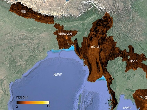
The researchers used Sentinel-2 satellite images from the European Space Agency (ESA) that are publicly available. They split these images into small six-square-kilometer grids. At this zoom level, visual information such as buildings, roads, and greenery can be used to quantify economic indicators. As a result, the team obtained the first ever fine-grained economic map of regions like North Korea. The same algorithm was applied to other underdeveloped countries in Asia: North Korea, Nepal, Laos, Myanmar, Bangladesh, and Cambodia (see Image 1).
The key feature of their research model is the "human-machine collaborative approach," which lets researchers combine human input with AI predictions for areas with scarce data. In this research, ten human experts compared satellite images and judged the economic conditions in the area, with the AI learning from this human data and giving economic scores to each image. The results showed that the Human-AI collaborative approach outperformed machine-only learning algorithms.
< Image 1. Nightlight satellite images of North Korea (Top-left: Background photo provided by NASA's Earth Observatory). South Korea appears brightly lit compared to North Korea, which is mostly dark except for Pyongyang. In contrast, the model developed by the research team uses daytime satellite imagery to predict more detailed economic predictions for North Korea (top-right) and five Asian countries (Bottom: Background photo from Google Earth). >
The research was led by an interdisciplinary team of computer scientists, economists, and a geographer from KAIST & IBS (Donghyun Ahn, Meeyoung Cha, Jihee Kim), Sogang University (Hyunjoo Yang), HKUST (Sangyoon Park), and NUS (Jeasurk Yang). Dr Charles Axelsson, Associate Editor at Nature Communications, handled this paper during the peer review process at the journal.
The research team found that the scores showed a strong correlation with traditional socio-economic metrics such as population density, employment, and number of businesses. This demonstrates the wide applicability and scalability of the approach, particularly in data-scarce countries. Furthermore, the model's strength lies in its ability to detect annual changes in economic conditions at a more detailed geospatial level without using any survey data (see Image 2).
< Image 2. Differences in satellite imagery and economic scores in North Korea between 2016 and 2019. Significant development was found in the Wonsan Kalma area (top), one of the tourist development zones, but no changes were observed in the Wiwon Industrial Development Zone (bottom). (Background photo: Sentinel-2 satellite imagery provided by the European Space Agency (ESA)). >
This model would be especially valuable for rapidly monitoring the progress of Sustainable Development Goals such as reducing poverty and promoting more equitable and sustainable growth on an international scale. The model can also be adapted to measure various social and environmental indicators. For example, it can be trained to identify regions with high vulnerability to climate change and disasters to provide timely guidance on disaster relief efforts.
As an example, the researchers explored how North Korea changed before and after the United Nations sanctions against the country. By applying the model to satellite images of North Korea both in 2016 and in 2019, the researchers discovered three key trends in the country's economic development between 2016 and 2019. First, economic growth in North Korea became more concentrated in Pyongyang and major cities, exacerbating the urban-rural divide. Second, satellite imagery revealed significant changes in areas designated for tourism and economic development, such as new building construction and other meaningful alterations. Third, traditional industrial and export development zones showed relatively minor changes.
Meeyoung Cha, a data scientist in the team explained, "This is an important interdisciplinary effort to address global challenges like poverty. We plan to apply our AI algorithm to other international issues, such as monitoring carbon emissions, disaster damage detection, and the impact of climate change."
An economist on the research team, Jihee Kim, commented that this approach would enable detailed examinations of economic conditions in the developing world at a low cost, reducing data disparities between developed and developing nations. She further emphasized that this is most essential because many public policies require economic measurements to achieve their goals, whether they are for growth, equality, or sustainability.
The research team has made the source code publicly available via GitHub and plans to continue improving the technology, applying it to new satellite images updated annually. The results of this study, with Ph.D. candidate Donghyun Ahn at KAIST and Ph.D. candidate Jeasurk Yang at NUS as joint first authors, were published in Nature Communications under the title "A human-machine collaborative approach measures economic development using satellite imagery."
< Photos of the main authors. 1. Donghyun Ahn, PhD candidate at KAIST School of Computing 2. Jeasurk Yang, PhD candidate at the Department of Geography of National University of Singapore 3. Meeyoung Cha, Professor of KAIST School of Computing and CI at IBS 4. Jihee Kim, Professor of KAIST School of Business and Technology Management 5. Sangyoon Park, Professor of the Division of Social Science at Hong Kong University of Science and Technology 6. Hyunjoo Yang, Professor of the Department of Economics at Sogang University >
2023.12.07 View 2628
North Korea and Beyond: AI-Powered Satellite Analysis Reveals the Unseen Economic Landscape of Underdeveloped Nations
- A joint research team in computer science, economics, and geography has developed an artificial intelligence (AI) technology to measure grid-level economic development within six-square-kilometer regions.
- This AI technology is applicable in regions with limited statistical data (e.g., North Korea), supporting international efforts to propose policies for economic growth and poverty reduction in underdeveloped countries.
- The research team plans to make this technology freely available for use to contribute to the United Nations' Sustainable Development Goals (SDGs).
The United Nations reports that more than 700 million people are in extreme poverty, earning less than two dollars a day. However, an accurate assessment of poverty remains a global challenge. For example, 53 countries have not conducted agricultural surveys in the past 15 years, and 17 countries have not published a population census. To fill this data gap, new technologies are being explored to estimate poverty using alternative sources such as street views, aerial photos, and satellite images.
The paper published in Nature Communications demonstrates how artificial intelligence (AI) can help analyze economic conditions from daytime satellite imagery. This new technology can even apply to the least developed countries - such as North Korea - that do not have reliable statistical data for typical machine learning training.
The researchers used Sentinel-2 satellite images from the European Space Agency (ESA) that are publicly available. They split these images into small six-square-kilometer grids. At this zoom level, visual information such as buildings, roads, and greenery can be used to quantify economic indicators. As a result, the team obtained the first ever fine-grained economic map of regions like North Korea. The same algorithm was applied to other underdeveloped countries in Asia: North Korea, Nepal, Laos, Myanmar, Bangladesh, and Cambodia (see Image 1).
The key feature of their research model is the "human-machine collaborative approach," which lets researchers combine human input with AI predictions for areas with scarce data. In this research, ten human experts compared satellite images and judged the economic conditions in the area, with the AI learning from this human data and giving economic scores to each image. The results showed that the Human-AI collaborative approach outperformed machine-only learning algorithms.
< Image 1. Nightlight satellite images of North Korea (Top-left: Background photo provided by NASA's Earth Observatory). South Korea appears brightly lit compared to North Korea, which is mostly dark except for Pyongyang. In contrast, the model developed by the research team uses daytime satellite imagery to predict more detailed economic predictions for North Korea (top-right) and five Asian countries (Bottom: Background photo from Google Earth). >
The research was led by an interdisciplinary team of computer scientists, economists, and a geographer from KAIST & IBS (Donghyun Ahn, Meeyoung Cha, Jihee Kim), Sogang University (Hyunjoo Yang), HKUST (Sangyoon Park), and NUS (Jeasurk Yang). Dr Charles Axelsson, Associate Editor at Nature Communications, handled this paper during the peer review process at the journal.
The research team found that the scores showed a strong correlation with traditional socio-economic metrics such as population density, employment, and number of businesses. This demonstrates the wide applicability and scalability of the approach, particularly in data-scarce countries. Furthermore, the model's strength lies in its ability to detect annual changes in economic conditions at a more detailed geospatial level without using any survey data (see Image 2).
< Image 2. Differences in satellite imagery and economic scores in North Korea between 2016 and 2019. Significant development was found in the Wonsan Kalma area (top), one of the tourist development zones, but no changes were observed in the Wiwon Industrial Development Zone (bottom). (Background photo: Sentinel-2 satellite imagery provided by the European Space Agency (ESA)). >
This model would be especially valuable for rapidly monitoring the progress of Sustainable Development Goals such as reducing poverty and promoting more equitable and sustainable growth on an international scale. The model can also be adapted to measure various social and environmental indicators. For example, it can be trained to identify regions with high vulnerability to climate change and disasters to provide timely guidance on disaster relief efforts.
As an example, the researchers explored how North Korea changed before and after the United Nations sanctions against the country. By applying the model to satellite images of North Korea both in 2016 and in 2019, the researchers discovered three key trends in the country's economic development between 2016 and 2019. First, economic growth in North Korea became more concentrated in Pyongyang and major cities, exacerbating the urban-rural divide. Second, satellite imagery revealed significant changes in areas designated for tourism and economic development, such as new building construction and other meaningful alterations. Third, traditional industrial and export development zones showed relatively minor changes.
Meeyoung Cha, a data scientist in the team explained, "This is an important interdisciplinary effort to address global challenges like poverty. We plan to apply our AI algorithm to other international issues, such as monitoring carbon emissions, disaster damage detection, and the impact of climate change."
An economist on the research team, Jihee Kim, commented that this approach would enable detailed examinations of economic conditions in the developing world at a low cost, reducing data disparities between developed and developing nations. She further emphasized that this is most essential because many public policies require economic measurements to achieve their goals, whether they are for growth, equality, or sustainability.
The research team has made the source code publicly available via GitHub and plans to continue improving the technology, applying it to new satellite images updated annually. The results of this study, with Ph.D. candidate Donghyun Ahn at KAIST and Ph.D. candidate Jeasurk Yang at NUS as joint first authors, were published in Nature Communications under the title "A human-machine collaborative approach measures economic development using satellite imagery."
< Photos of the main authors. 1. Donghyun Ahn, PhD candidate at KAIST School of Computing 2. Jeasurk Yang, PhD candidate at the Department of Geography of National University of Singapore 3. Meeyoung Cha, Professor of KAIST School of Computing and CI at IBS 4. Jihee Kim, Professor of KAIST School of Business and Technology Management 5. Sangyoon Park, Professor of the Division of Social Science at Hong Kong University of Science and Technology 6. Hyunjoo Yang, Professor of the Department of Economics at Sogang University >
2023.12.07 View 2628 -
 KAIST-UCSD researchers build an enzyme discovering AI
- A joint research team led by Distinguished Professor Sang Yup Lee of the Department of Chemical and Biomolecular Engineering and Bernhard Palsson of UCSD developed ‘DeepECtransformer’, an artificial intelligence that can predict Enzyme Commission (EC) number of proteins.
- The AI is tasked to discover new enzymes that have not been discovered yet, which would allow prediction for a total of 5,360 types of Enzyme Commission (EC) numbers
- It is expected to be used in the development of microbial cell factories that produce environmentally friendly chemicals as a core technology for analyzing the metabolic network of a genome.
While E. coli is one of the most studied organisms, the function of 30% of proteins that make up E. coli has not yet been clearly revealed. For this, an artificial intelligence was used to discover 464 types of enzymes from the proteins that were unknown, and the researchers went on to verify the predictions of 3 types of proteins were successfully identified through in vitro enzyme assay.
KAIST (President Kwang-Hyung Lee) announced on the 24th that a joint research team comprised of Gi Bae Kim, Ji Yeon Kim, Dr. Jong An Lee and Distinguished Professor Sang Yup Lee of the Department of Chemical and Biomolecular Engineering at KAIST, and Dr. Charles J. Norsigian and Professor Bernhard O. Palsson of the Department of Bioengineering at UCSD has developed DeepECtransformer, an artificial intelligence that can predict the enzyme functions from the protein sequence, and has established a prediction system by utilizing the AI to quickly and accurately identify the enzyme function.
Enzymes are proteins that catalyze biological reactions, and identifying the function of each enzyme is essential to understanding the various chemical reactions that exist in living organisms and the metabolic characteristics of those organisms. Enzyme Commission (EC) number is an enzyme function classification system designed by the International Union of Biochemistry and Molecular Biology, and in order to understand the metabolic characteristics of various organisms, it is necessary to develop a technology that can quickly analyze enzymes and EC numbers of the enzymes present in the genome.
Various methodologies based on deep learning have been developed to analyze the features of biological sequences, including protein function prediction, but most of them have a problem of a black box, where the inference process of AI cannot be interpreted. Various prediction systems that utilize AI for enzyme function prediction have also been reported, but they do not solve this black box problem, or cannot interpret the reasoning process in fine-grained level (e.g., the level of amino acid residues in the enzyme sequence).
The joint team developed DeepECtransformer, an AI that utilizes deep learning and a protein homology analysis module to predict the enzyme function of a given protein sequence. To better understand the features of protein sequences, the transformer architecture, which is commonly used in natural language processing, was additionally used to extract important features about enzyme functions in the context of the entire protein sequence, which enabled the team to accurately predict the EC number of the enzyme. The developed DeepECtransformer can predict a total of 5360 EC numbers.
The joint team further analyzed the transformer architecture to understand the inference process of DeepECtransformer, and found that in the inference process, the AI utilizes information on catalytic active sites and/or the cofactor binding sites which are important for enzyme function. By analyzing the black box of DeepECtransformer, it was confirmed that the AI was able to identify the features that are important for enzyme function on its own during the learning process.
"By utilizing the prediction system we developed, we were able to predict the functions of enzymes that had not yet been identified and verify them experimentally," said Gi Bae Kim, the first author of the paper. "By using DeepECtransformer to identify previously unknown enzymes in living organisms, we will be able to more accurately analyze various facets involved in the metabolic processes of organisms, such as the enzymes needed to biosynthesize various useful compounds or the enzymes needed to biodegrade plastics." he added.
"DeepECtransformer, which quickly and accurately predicts enzyme functions, is a key technology in functional genomics, enabling us to analyze the function of entire enzymes at the systems level," said Professor Sang Yup Lee. He added, “We will be able to use it to develop eco-friendly microbial factories based on comprehensive genome-scale metabolic models, potentially minimizing missing information of metabolism.”
The joint team’s work on DeepECtransformer is described in the paper titled "Functional annotation of enzyme-encoding genes using deep learning with transformer layers" written by Gi Bae Kim, Professor Sang Yup Lee of the Department of Chemical and Biomolecular Engineering of KAIST and their colleagues. The paper was published via peer-review on the 14th of November on “Nature Communications”.
This research was conducted with the support by “the Development of next-generation biorefinery platform technologies for leading bio-based chemicals industry project (2022M3J5A1056072)” and by “Development of platform technologies of microbial cell factories for the next-generation biorefineries project (2022M3J5A1056117)” from National Research Foundation supported by the Korean Ministry of Science and ICT (Project Leader: Distinguished Professor Sang Yup Lee, KAIST).
< Figure 1. The structure of DeepECtransformer's artificial neural network >
2023.11.24 View 1889
KAIST-UCSD researchers build an enzyme discovering AI
- A joint research team led by Distinguished Professor Sang Yup Lee of the Department of Chemical and Biomolecular Engineering and Bernhard Palsson of UCSD developed ‘DeepECtransformer’, an artificial intelligence that can predict Enzyme Commission (EC) number of proteins.
- The AI is tasked to discover new enzymes that have not been discovered yet, which would allow prediction for a total of 5,360 types of Enzyme Commission (EC) numbers
- It is expected to be used in the development of microbial cell factories that produce environmentally friendly chemicals as a core technology for analyzing the metabolic network of a genome.
While E. coli is one of the most studied organisms, the function of 30% of proteins that make up E. coli has not yet been clearly revealed. For this, an artificial intelligence was used to discover 464 types of enzymes from the proteins that were unknown, and the researchers went on to verify the predictions of 3 types of proteins were successfully identified through in vitro enzyme assay.
KAIST (President Kwang-Hyung Lee) announced on the 24th that a joint research team comprised of Gi Bae Kim, Ji Yeon Kim, Dr. Jong An Lee and Distinguished Professor Sang Yup Lee of the Department of Chemical and Biomolecular Engineering at KAIST, and Dr. Charles J. Norsigian and Professor Bernhard O. Palsson of the Department of Bioengineering at UCSD has developed DeepECtransformer, an artificial intelligence that can predict the enzyme functions from the protein sequence, and has established a prediction system by utilizing the AI to quickly and accurately identify the enzyme function.
Enzymes are proteins that catalyze biological reactions, and identifying the function of each enzyme is essential to understanding the various chemical reactions that exist in living organisms and the metabolic characteristics of those organisms. Enzyme Commission (EC) number is an enzyme function classification system designed by the International Union of Biochemistry and Molecular Biology, and in order to understand the metabolic characteristics of various organisms, it is necessary to develop a technology that can quickly analyze enzymes and EC numbers of the enzymes present in the genome.
Various methodologies based on deep learning have been developed to analyze the features of biological sequences, including protein function prediction, but most of them have a problem of a black box, where the inference process of AI cannot be interpreted. Various prediction systems that utilize AI for enzyme function prediction have also been reported, but they do not solve this black box problem, or cannot interpret the reasoning process in fine-grained level (e.g., the level of amino acid residues in the enzyme sequence).
The joint team developed DeepECtransformer, an AI that utilizes deep learning and a protein homology analysis module to predict the enzyme function of a given protein sequence. To better understand the features of protein sequences, the transformer architecture, which is commonly used in natural language processing, was additionally used to extract important features about enzyme functions in the context of the entire protein sequence, which enabled the team to accurately predict the EC number of the enzyme. The developed DeepECtransformer can predict a total of 5360 EC numbers.
The joint team further analyzed the transformer architecture to understand the inference process of DeepECtransformer, and found that in the inference process, the AI utilizes information on catalytic active sites and/or the cofactor binding sites which are important for enzyme function. By analyzing the black box of DeepECtransformer, it was confirmed that the AI was able to identify the features that are important for enzyme function on its own during the learning process.
"By utilizing the prediction system we developed, we were able to predict the functions of enzymes that had not yet been identified and verify them experimentally," said Gi Bae Kim, the first author of the paper. "By using DeepECtransformer to identify previously unknown enzymes in living organisms, we will be able to more accurately analyze various facets involved in the metabolic processes of organisms, such as the enzymes needed to biosynthesize various useful compounds or the enzymes needed to biodegrade plastics." he added.
"DeepECtransformer, which quickly and accurately predicts enzyme functions, is a key technology in functional genomics, enabling us to analyze the function of entire enzymes at the systems level," said Professor Sang Yup Lee. He added, “We will be able to use it to develop eco-friendly microbial factories based on comprehensive genome-scale metabolic models, potentially minimizing missing information of metabolism.”
The joint team’s work on DeepECtransformer is described in the paper titled "Functional annotation of enzyme-encoding genes using deep learning with transformer layers" written by Gi Bae Kim, Professor Sang Yup Lee of the Department of Chemical and Biomolecular Engineering of KAIST and their colleagues. The paper was published via peer-review on the 14th of November on “Nature Communications”.
This research was conducted with the support by “the Development of next-generation biorefinery platform technologies for leading bio-based chemicals industry project (2022M3J5A1056072)” and by “Development of platform technologies of microbial cell factories for the next-generation biorefineries project (2022M3J5A1056117)” from National Research Foundation supported by the Korean Ministry of Science and ICT (Project Leader: Distinguished Professor Sang Yup Lee, KAIST).
< Figure 1. The structure of DeepECtransformer's artificial neural network >
2023.11.24 View 1889 -
 NYU-KAIST Global AI & Digital Governance Conference Held
< Photo 1. Opening of NYU-KAIST Global AI & Digital Governance Conference >
In attendance of the Minister of Science and ICT Jong-ho Lee, NYU President Linda G. Mills, and KAIST President Kwang Hyung Lee, KAIST co-hosted the NYU-KAIST Global AI & Digital Governance Conference at the Paulson Center of New York University (NYU) in New York City, USA on September 21st, 9:30 pm.
At the conference, KAIST and NYU discussed the direction and policies for ‘global AI and digital governance’ with participants of upto 300 people which includes scholars, professors, and students involved in the academic field of AI and digitalization from both Korea and the United States and other international backgrounds. This conference was a forum of an international discussion that sought new directions for AI and digital technology take in the future and gathered consensus on regulations.
Following a welcoming address by KAIST President, Kwang Hyung Lee and a congratulatory message from the Minister of Science and ICT, Jong-ho Lee, a panel discussion was held, moderated by Professor Matthew Liao, a graduate of Princeton and Oxford University, currently serving as a professor at NYU and the director at the Center for Bioethics of the NYU School of Global Public Health.
Six prominent scholars took part in the panel discussion. Prof. Kyung-hyun Cho of NYU Applied Mathematics and Data Science Center, a KAIST graduate who has joined the ranks of the world-class in AI language models and Professor Jong Chul Ye, the Director of Promotion Council for Digital Health at KAIST, who is leading innovative research in the field of medical AI working in collaboration with major hospitals at home and abroad was on the panel. Additionally, Professor Luciano Floridi, a founding member of the Yale University Center for Digital Ethics, Professor Shannon Vallor, the Baillie Gifford Professor in the Ethics of Data and Artificial Intelligence at the University of Edinburgh of the UK, Professor Stefaan Verhulst, a Co-Founder and the DIrector of GovLab‘s Data Program at NYU’s Tandon School of Engineering, and Professor Urs Gasser, who is in charge of public policy, governance and innovative technology at the Technical University of Munich, also participated.
Professor Matthew Liao from NYU led the discussion on various topics such as the ways to to regulate AI and digital technologies; the concerns about how deep learning technology being developed in medicinal purposes could be used in warfare; the scope of responsibilities Al scientists' responsibility should carry in ensuring the usage of AI are limited to benign purposes only; the effects of external regulation on the AI model developers and the research they pursue; and on the lessons that can be learned from the regulations in other fields.
During the panel discussion, there was an exchange of ideas about a system of standards that could harmonize digital development and regulatory and social ethics in today’s situation in which digital transformation accelerates technological development at a global level, there is a looming concern that while such advancements are bringing economic vitality it may create digital divides and probles like manipulation of public opinion. Professor Jong-cheol Ye of KAIST (Director of the Promotion Council for Digital Health), in particular, emphasized that it is important to find a point of balance that does not hinder the advancements rather than opting to enforcing strict regulations.
< Photo 2. Panel Discussion in Session at NYU-KAIST Global AI & Digital Governance Conference >
KAIST President Kwang Hyung Lee explained, “At the Digital Governance Forum we had last October, we focused on exploring new governance to solve digital challenges in the time of global digital transition, and this year’s main focus was on regulations.”
“This conference served as an opportunity of immense value as we came to understand that appropriate regulations can be a motivation to spur further developments rather than a hurdle when it comes to technological advancements, and that it is important for us to clearly understand artificial intelligence and consider what should and can be regulated when we are to set regulations on artificial intelligence,” he continued.
Earlier, KAIST signed a cooperation agreement with NYU to build a joint campus, June last year and held a plaque presentation ceremony for the KAIST NYU Joint Campus last September to promote joint research between the two universities. KAIST is currently conducting joint research with NYU in nine fields, including AI and digital research. The KAIST-NYU Joint Campus was conceived with the goal of building an innovative sandbox campus centering aroung science, technology, engineering, and mathematics (STEM) combining NYU's excellent humanities and arts as well as basic science and convergence research capabilities with KAIST's science and technology.
KAIST has contributed to the development of Korea's industry and economy through technological innovation aiding in the nation’s transformation into an innovative nation with scientific and technological prowess. KAIST will now pursue an anchor/base strategy to raise KAIST's awareness in New York through the NYU Joint Campus by establishing a KAIST campus within the campus of NYU, the heart of New York.
2023.09.22 View 3700
NYU-KAIST Global AI & Digital Governance Conference Held
< Photo 1. Opening of NYU-KAIST Global AI & Digital Governance Conference >
In attendance of the Minister of Science and ICT Jong-ho Lee, NYU President Linda G. Mills, and KAIST President Kwang Hyung Lee, KAIST co-hosted the NYU-KAIST Global AI & Digital Governance Conference at the Paulson Center of New York University (NYU) in New York City, USA on September 21st, 9:30 pm.
At the conference, KAIST and NYU discussed the direction and policies for ‘global AI and digital governance’ with participants of upto 300 people which includes scholars, professors, and students involved in the academic field of AI and digitalization from both Korea and the United States and other international backgrounds. This conference was a forum of an international discussion that sought new directions for AI and digital technology take in the future and gathered consensus on regulations.
Following a welcoming address by KAIST President, Kwang Hyung Lee and a congratulatory message from the Minister of Science and ICT, Jong-ho Lee, a panel discussion was held, moderated by Professor Matthew Liao, a graduate of Princeton and Oxford University, currently serving as a professor at NYU and the director at the Center for Bioethics of the NYU School of Global Public Health.
Six prominent scholars took part in the panel discussion. Prof. Kyung-hyun Cho of NYU Applied Mathematics and Data Science Center, a KAIST graduate who has joined the ranks of the world-class in AI language models and Professor Jong Chul Ye, the Director of Promotion Council for Digital Health at KAIST, who is leading innovative research in the field of medical AI working in collaboration with major hospitals at home and abroad was on the panel. Additionally, Professor Luciano Floridi, a founding member of the Yale University Center for Digital Ethics, Professor Shannon Vallor, the Baillie Gifford Professor in the Ethics of Data and Artificial Intelligence at the University of Edinburgh of the UK, Professor Stefaan Verhulst, a Co-Founder and the DIrector of GovLab‘s Data Program at NYU’s Tandon School of Engineering, and Professor Urs Gasser, who is in charge of public policy, governance and innovative technology at the Technical University of Munich, also participated.
Professor Matthew Liao from NYU led the discussion on various topics such as the ways to to regulate AI and digital technologies; the concerns about how deep learning technology being developed in medicinal purposes could be used in warfare; the scope of responsibilities Al scientists' responsibility should carry in ensuring the usage of AI are limited to benign purposes only; the effects of external regulation on the AI model developers and the research they pursue; and on the lessons that can be learned from the regulations in other fields.
During the panel discussion, there was an exchange of ideas about a system of standards that could harmonize digital development and regulatory and social ethics in today’s situation in which digital transformation accelerates technological development at a global level, there is a looming concern that while such advancements are bringing economic vitality it may create digital divides and probles like manipulation of public opinion. Professor Jong-cheol Ye of KAIST (Director of the Promotion Council for Digital Health), in particular, emphasized that it is important to find a point of balance that does not hinder the advancements rather than opting to enforcing strict regulations.
< Photo 2. Panel Discussion in Session at NYU-KAIST Global AI & Digital Governance Conference >
KAIST President Kwang Hyung Lee explained, “At the Digital Governance Forum we had last October, we focused on exploring new governance to solve digital challenges in the time of global digital transition, and this year’s main focus was on regulations.”
“This conference served as an opportunity of immense value as we came to understand that appropriate regulations can be a motivation to spur further developments rather than a hurdle when it comes to technological advancements, and that it is important for us to clearly understand artificial intelligence and consider what should and can be regulated when we are to set regulations on artificial intelligence,” he continued.
Earlier, KAIST signed a cooperation agreement with NYU to build a joint campus, June last year and held a plaque presentation ceremony for the KAIST NYU Joint Campus last September to promote joint research between the two universities. KAIST is currently conducting joint research with NYU in nine fields, including AI and digital research. The KAIST-NYU Joint Campus was conceived with the goal of building an innovative sandbox campus centering aroung science, technology, engineering, and mathematics (STEM) combining NYU's excellent humanities and arts as well as basic science and convergence research capabilities with KAIST's science and technology.
KAIST has contributed to the development of Korea's industry and economy through technological innovation aiding in the nation’s transformation into an innovative nation with scientific and technological prowess. KAIST will now pursue an anchor/base strategy to raise KAIST's awareness in New York through the NYU Joint Campus by establishing a KAIST campus within the campus of NYU, the heart of New York.
2023.09.22 View 3700 -
 KAIST holds its first ‘KAIST Tech Fair’ in New York, USA
< Photo 1. 2023 KAIST Tech Fair in New York >
KAIST (President Kwang-Hyung Lee) announced on the 11th that it will hold the ‘2023 KAIST Tech Fair in New York’ at the Kimmel Center at New York University in Manhattan, USA, on the 22nd of this month. It is an event designed to be the starting point for KAIST to expand its startup ecosystem into the global stage, and it is to attract investments and secure global customers in New York by demonstrating the technological value of KAIST startup companies directly at location.
< Photo 2. President Kwang Hyung Lee at the 2023 KAIST Tech Fair in New York >
KAIST has been holding briefing sessions for technology transfer in Korea every year since 2018, and this year is the first time to hold a tech fair overseas for global companies.
KAIST Institute of Technology Value Creation (Director Sung-Yool Choi) has prepared for this event over the past six months with the Korea International Trade Association (hereinafter KITA, CEO Christopher Koo) to survey customer base and investment companies to conduct market analysis.
Among the companies founded with the technologies developed by the faculty and students of KAIST and their partners, 7 companies were selected to be matched with companies overseas that expressed interests in these technologies. Global multinational companies in the fields of IT, artificial intelligence, environment, logistics, distribution, and retail are participating as demand agencies and are testing the marketability of the start-up's technology as of September.
Daim Research, founded by Professor Young Jae Jang of the Department of Industrial and Systems Engineering, is a company specializing in smart factory automation solutions and is knocking on the door of the global market with a platform technology optimized for automated logistics systems.
< Photo 3. Presentation by Professor Young Jae Jang for DAIM Research >
It is a ‘collaborative intelligence’ solution that maximizes work productivity by having a number of robots used in industrial settings collaborate with one another. The strength of their solution is that logistics robots equipped with AI reinforced learning technology can respond to processes and environmental changes on their own, minimizing maintenance costs and the system can achieve excellent performance even with a small amount of data when it is combined with the digital twin technology the company has developed on its own.
A student startup, ‘Aniai’, is entering the US market, the home of hamburgers, with hamburger patty automation equipments and solutions. This is a robot kitchen startup founded by its CEO Gunpil Hwang, a graduate of KAIST’s School of Electrical Engineering which gathered together the experts in the fields of robot control, design, and artificial intelligence and cognitive technology to develop technology to automatically cook hamburger patties.
At the touch of a button, both sides of the patty are cooked simultaneously for consistent taste and quality according to the set condition. Since it can cook about 200 dishes in an hour, it is attracting attention as a technology that can not only solve manpower shortages but also accelerate the digital transformation of the restaurant industry.
Also, at the tech fair to be held at the Kimmel Center of New York University on the 22nd, the following startups who are currently under market verification in the U.S. will be participating: ▴'TheWaveTalk', which developed a water quality management system that can measure external substances and metal ions by transferring original technology from KAIST; ▴‘VIRNECT’, which helps workers improve their skills by remotely managing industrial sites using XR*; ▴‘Datumo’, a solution that helps process and analyze artificial intelligence big data, ▴‘VESSL AI’, the provider of a solution to eliminate the overhead** of machine learning systems; and ▴ ‘DolbomDream’, which developed an inflatable vest that helps the psychological stability of people with developmental disabilities.
* XR (eXtended Reality): Ultra-realistic technology that enhances immersion by utilizing augmented reality, virtual reality, and mixed reality technologies
** Overhead: Additional time required for stable processing of the program
In addition, two companies (Plasmapp and NotaAI) that are participating in the D-Unicorn program with the support of the Daejeon City and two companies (Enget and ILIAS Biologics) that are receiving support from the Scale Up Tips of the Ministry of SMEs and Startups, three companies (WiPowerOne, IDK Lab, and Artificial Photosynthesis Lab) that are continuing to realize the sustainable development goals for a total of 14 KAIST startups, will hold a corporate information session with about 100 invited guests from global companies and venture capital.
< Photo 4. Presentation for AP Lab >
Prior to this event, participating startups will be visiting the New York Economic Development Corporation and large law firms to receive advice on U.S. government support programs and on their attemps to enter the U.S. market. In addition, the participating companies plan to visit a startup support investment institution pursuing sustainable development goals and the Leslie eLab, New York University's one-stop startup support space, to lay the foundation for KAIST's leap forward in global technology commercialization.
< Photo 5. Sung-Yool Choi, the Director of KAIST Institute of Technology Value Creation (left) at the 2023 KAIST Tech Fair in New York with the key participants >
Sung-Yool Choi, the Director of KAIST Institute of Technology Value Creation, said, “KAIST prepared this event to realize its vision of being a leading university in creating global value.” He added, “We hope that our startups founded with KAIST technology would successfully completed market verification to be successful in securing global demands and in attracting investments for their endeavors.”
2023.09.11 View 6701
KAIST holds its first ‘KAIST Tech Fair’ in New York, USA
< Photo 1. 2023 KAIST Tech Fair in New York >
KAIST (President Kwang-Hyung Lee) announced on the 11th that it will hold the ‘2023 KAIST Tech Fair in New York’ at the Kimmel Center at New York University in Manhattan, USA, on the 22nd of this month. It is an event designed to be the starting point for KAIST to expand its startup ecosystem into the global stage, and it is to attract investments and secure global customers in New York by demonstrating the technological value of KAIST startup companies directly at location.
< Photo 2. President Kwang Hyung Lee at the 2023 KAIST Tech Fair in New York >
KAIST has been holding briefing sessions for technology transfer in Korea every year since 2018, and this year is the first time to hold a tech fair overseas for global companies.
KAIST Institute of Technology Value Creation (Director Sung-Yool Choi) has prepared for this event over the past six months with the Korea International Trade Association (hereinafter KITA, CEO Christopher Koo) to survey customer base and investment companies to conduct market analysis.
Among the companies founded with the technologies developed by the faculty and students of KAIST and their partners, 7 companies were selected to be matched with companies overseas that expressed interests in these technologies. Global multinational companies in the fields of IT, artificial intelligence, environment, logistics, distribution, and retail are participating as demand agencies and are testing the marketability of the start-up's technology as of September.
Daim Research, founded by Professor Young Jae Jang of the Department of Industrial and Systems Engineering, is a company specializing in smart factory automation solutions and is knocking on the door of the global market with a platform technology optimized for automated logistics systems.
< Photo 3. Presentation by Professor Young Jae Jang for DAIM Research >
It is a ‘collaborative intelligence’ solution that maximizes work productivity by having a number of robots used in industrial settings collaborate with one another. The strength of their solution is that logistics robots equipped with AI reinforced learning technology can respond to processes and environmental changes on their own, minimizing maintenance costs and the system can achieve excellent performance even with a small amount of data when it is combined with the digital twin technology the company has developed on its own.
A student startup, ‘Aniai’, is entering the US market, the home of hamburgers, with hamburger patty automation equipments and solutions. This is a robot kitchen startup founded by its CEO Gunpil Hwang, a graduate of KAIST’s School of Electrical Engineering which gathered together the experts in the fields of robot control, design, and artificial intelligence and cognitive technology to develop technology to automatically cook hamburger patties.
At the touch of a button, both sides of the patty are cooked simultaneously for consistent taste and quality according to the set condition. Since it can cook about 200 dishes in an hour, it is attracting attention as a technology that can not only solve manpower shortages but also accelerate the digital transformation of the restaurant industry.
Also, at the tech fair to be held at the Kimmel Center of New York University on the 22nd, the following startups who are currently under market verification in the U.S. will be participating: ▴'TheWaveTalk', which developed a water quality management system that can measure external substances and metal ions by transferring original technology from KAIST; ▴‘VIRNECT’, which helps workers improve their skills by remotely managing industrial sites using XR*; ▴‘Datumo’, a solution that helps process and analyze artificial intelligence big data, ▴‘VESSL AI’, the provider of a solution to eliminate the overhead** of machine learning systems; and ▴ ‘DolbomDream’, which developed an inflatable vest that helps the psychological stability of people with developmental disabilities.
* XR (eXtended Reality): Ultra-realistic technology that enhances immersion by utilizing augmented reality, virtual reality, and mixed reality technologies
** Overhead: Additional time required for stable processing of the program
In addition, two companies (Plasmapp and NotaAI) that are participating in the D-Unicorn program with the support of the Daejeon City and two companies (Enget and ILIAS Biologics) that are receiving support from the Scale Up Tips of the Ministry of SMEs and Startups, three companies (WiPowerOne, IDK Lab, and Artificial Photosynthesis Lab) that are continuing to realize the sustainable development goals for a total of 14 KAIST startups, will hold a corporate information session with about 100 invited guests from global companies and venture capital.
< Photo 4. Presentation for AP Lab >
Prior to this event, participating startups will be visiting the New York Economic Development Corporation and large law firms to receive advice on U.S. government support programs and on their attemps to enter the U.S. market. In addition, the participating companies plan to visit a startup support investment institution pursuing sustainable development goals and the Leslie eLab, New York University's one-stop startup support space, to lay the foundation for KAIST's leap forward in global technology commercialization.
< Photo 5. Sung-Yool Choi, the Director of KAIST Institute of Technology Value Creation (left) at the 2023 KAIST Tech Fair in New York with the key participants >
Sung-Yool Choi, the Director of KAIST Institute of Technology Value Creation, said, “KAIST prepared this event to realize its vision of being a leading university in creating global value.” He added, “We hope that our startups founded with KAIST technology would successfully completed market verification to be successful in securing global demands and in attracting investments for their endeavors.”
2023.09.11 View 6701 -
 KAIST builds a high-resolution 3D holographic sensor using a single mask
Holographic cameras can provide more realistic images than ordinary cameras thanks to their ability to acquire 3D information about objects. However, existing holographic cameras use interferometers that measure the wavelength and refraction of light through the interference of light waves, which makes them complex and sensitive to their surrounding environment.
On August 23, a KAIST research team led by Professor YongKeun Park from the Department of Physics announced a new leap forward in 3D holographic imaging sensor technology.
The team proposed an innovative holographic camera technology that does not use complex interferometry. Instead, it uses a mask to precisely measure the phase information of light and reconstruct the 3D information of an object with higher accuracy.
< Figure 1. Structure and principle of the proposed holographic camera. The amplitude and phase information of light scattered from a holographic camera can be measured. >
The team used a mask that fulfills certain mathematical conditions and incorporated it into an ordinary camera, and the light scattered from a laser is measured through the mask and analyzed using a computer. This does not require a complex interferometer and allows the phase information of light to be collected through a simplified optical system. With this technique, the mask that is placed between the two lenses and behind an object plays an important role. The mask selectively filters specific parts of light,, and the intensity of the light passing through the lens can be measured using an ordinary commercial camera. This technique combines the image data received from the camera with the unique pattern received from the mask and reconstructs an object’s precise 3D information using an algorithm.
This method allows a high-resolution 3D image of an object to be captured in any position. In practical situations, one can construct a laser-based holographic 3D image sensor by adding a mask with a simple design to a general image sensor. This makes the design and construction of the optical system much easier. In particular, this novel technology can capture high-resolution holographic images of objects moving at high speeds, which widens its potential field of application.
< Figure 2. A moving doll captured by a conventional camera and the proposed holographic camera. When taking a picture without focusing on the object, only a blurred image of the doll can be obtained from a general camera, but the proposed holographic camera can restore the blurred image of the doll into a clear image. >
The results of this study, conducted by Dr. Jeonghun Oh from the KAIST Department of Physics as the first author, were published in Nature Communications on August 12 under the title, "Non-interferometric stand-alone single-shot holographic camera using reciprocal diffractive imaging".
Dr. Oh said, “The holographic camera module we are suggesting can be built by adding a filter to an ordinary camera, which would allow even non-experts to handle it easily in everyday life if it were to be commercialized.” He added, “In particular, it is a promising candidate with the potential to replace existing remote sensing technologies.”
This research was supported by the National Research Foundation’s Leader Research Project, the Korean Ministry of Science and ICT’s Core Hologram Technology Support Project, and the Nano and Material Technology Development Project.
2023.09.05 View 2828
KAIST builds a high-resolution 3D holographic sensor using a single mask
Holographic cameras can provide more realistic images than ordinary cameras thanks to their ability to acquire 3D information about objects. However, existing holographic cameras use interferometers that measure the wavelength and refraction of light through the interference of light waves, which makes them complex and sensitive to their surrounding environment.
On August 23, a KAIST research team led by Professor YongKeun Park from the Department of Physics announced a new leap forward in 3D holographic imaging sensor technology.
The team proposed an innovative holographic camera technology that does not use complex interferometry. Instead, it uses a mask to precisely measure the phase information of light and reconstruct the 3D information of an object with higher accuracy.
< Figure 1. Structure and principle of the proposed holographic camera. The amplitude and phase information of light scattered from a holographic camera can be measured. >
The team used a mask that fulfills certain mathematical conditions and incorporated it into an ordinary camera, and the light scattered from a laser is measured through the mask and analyzed using a computer. This does not require a complex interferometer and allows the phase information of light to be collected through a simplified optical system. With this technique, the mask that is placed between the two lenses and behind an object plays an important role. The mask selectively filters specific parts of light,, and the intensity of the light passing through the lens can be measured using an ordinary commercial camera. This technique combines the image data received from the camera with the unique pattern received from the mask and reconstructs an object’s precise 3D information using an algorithm.
This method allows a high-resolution 3D image of an object to be captured in any position. In practical situations, one can construct a laser-based holographic 3D image sensor by adding a mask with a simple design to a general image sensor. This makes the design and construction of the optical system much easier. In particular, this novel technology can capture high-resolution holographic images of objects moving at high speeds, which widens its potential field of application.
< Figure 2. A moving doll captured by a conventional camera and the proposed holographic camera. When taking a picture without focusing on the object, only a blurred image of the doll can be obtained from a general camera, but the proposed holographic camera can restore the blurred image of the doll into a clear image. >
The results of this study, conducted by Dr. Jeonghun Oh from the KAIST Department of Physics as the first author, were published in Nature Communications on August 12 under the title, "Non-interferometric stand-alone single-shot holographic camera using reciprocal diffractive imaging".
Dr. Oh said, “The holographic camera module we are suggesting can be built by adding a filter to an ordinary camera, which would allow even non-experts to handle it easily in everyday life if it were to be commercialized.” He added, “In particular, it is a promising candidate with the potential to replace existing remote sensing technologies.”
This research was supported by the National Research Foundation’s Leader Research Project, the Korean Ministry of Science and ICT’s Core Hologram Technology Support Project, and the Nano and Material Technology Development Project.
2023.09.05 View 2828