CES
-
 KAIST's Doctoral Student Receives a Hoffman Scholarship Award
Hyo-Sun Lee, a doctoral student at the Graduate School of EEWS (Environment, Energy, Water and Sustainability), KAIST, is a recipient of the 2016 Dorothy M. and Earl S. Hoffman Scholarships presented by the American Vacuum Society (AVS). The award ceremony took place during the Society’s 63rd International Symposium and Exhibition on November 6-11, 2016 in Nashville, Tennessee.
Lee is the first Korean and foreign student to receive this scholarship.
The Hoffman Scholarships were established in 2002 to recognize and encourage excellence in graduate studies in the sciences and technologies of interest to AVS. The scholarships are funded by a bequest from Dorothy M. Hoffman, who was a pioneering member of the Society of Women Engineers and served as the president of AVS in 1974.
Lee received the scholarship for her research that detects hot electrons from chemical reactions on catalytic surface using nanodevices. Nano Letters, an academic journal published by the American Chemical Society, described her work in its February 2016 issue as a technology that allows quantitative analysis of hot electrons by employing a new nanodevice and therefore helps researchers understand better the mechanism of chemical reactions on nanocatalytic surface. She also published her work to detect the flow of hot electrons that occur on metal nanocatalytic surface during hydrogen oxidation reactions in Angewandte Chemie.
Lee said, “I am pleased to receive this honor from such a world-renowned academic society. Certainly, this will be a great support for my future study and research.”
Founded in 1953, AVS is an interdisciplinary, professional society composed of approximately 4,500 members worldwide. It supports networking among academic, industrial, government, and consulting professionals involved in a range of established and emerging science and technology areas such as chemistry, physics, engineering, business, and technology development.
2016.11.17 View 11116
KAIST's Doctoral Student Receives a Hoffman Scholarship Award
Hyo-Sun Lee, a doctoral student at the Graduate School of EEWS (Environment, Energy, Water and Sustainability), KAIST, is a recipient of the 2016 Dorothy M. and Earl S. Hoffman Scholarships presented by the American Vacuum Society (AVS). The award ceremony took place during the Society’s 63rd International Symposium and Exhibition on November 6-11, 2016 in Nashville, Tennessee.
Lee is the first Korean and foreign student to receive this scholarship.
The Hoffman Scholarships were established in 2002 to recognize and encourage excellence in graduate studies in the sciences and technologies of interest to AVS. The scholarships are funded by a bequest from Dorothy M. Hoffman, who was a pioneering member of the Society of Women Engineers and served as the president of AVS in 1974.
Lee received the scholarship for her research that detects hot electrons from chemical reactions on catalytic surface using nanodevices. Nano Letters, an academic journal published by the American Chemical Society, described her work in its February 2016 issue as a technology that allows quantitative analysis of hot electrons by employing a new nanodevice and therefore helps researchers understand better the mechanism of chemical reactions on nanocatalytic surface. She also published her work to detect the flow of hot electrons that occur on metal nanocatalytic surface during hydrogen oxidation reactions in Angewandte Chemie.
Lee said, “I am pleased to receive this honor from such a world-renowned academic society. Certainly, this will be a great support for my future study and research.”
Founded in 1953, AVS is an interdisciplinary, professional society composed of approximately 4,500 members worldwide. It supports networking among academic, industrial, government, and consulting professionals involved in a range of established and emerging science and technology areas such as chemistry, physics, engineering, business, and technology development.
2016.11.17 View 11116 -
 Key Interaction between the Circadian Clock and Cancer Identified
Professor Jae Kyoung Kim and his research team from the Department of Mathematical Sciences at KAIST found that the circadian clock drives changes in circadian rhythms of p53 which functions as a tumor suppressor. Using a differential equation, he applied a model-driven mathematical approach to learn the mechanism and role of p53.
Kim’s mathematical modeling has been validated by experimental studies conducted by a research team at Virginia Polytechnic Institute and State University (Virginia Tech) in the United State, which is led by Professor Carla Finkielstein. As a result, the researchers revealed that there is an important link existed between the circadian clock and cancer.
The findings of this research were published online in Proceedings of the National Academy of Sciences of the United States of the America (PNAS) on November 9, 2016.
The circadian clock in our brain controls behavioral and physiological processes within a period of 24 hours, including making us fall asleep at a certain time by triggering the release of the sleep hormone melatonin in our brain, for example, around 9 pm. The clock is also involved in various physiological processes such as cell division, movement, and development.
Disruptions caused by the mismatch of the circadian clock and real time due to chronic late night work, shiftwork, and other similar issues may lead to various diseases such as diabetes, cancer, and heart disease.
In 2014, when Kim met with Finkielstein, her research team succeeded in observing the changes of p53 over a period of 24 hours, but could not understand how the circadian clock controls the 24-hour rhythm of p53. It was difficult to determine p53’s mechanism since its cell regulation system is far more complex than other cells
To solve the problem, Kim set up a computer simulation using mathematical modeling and ran millions of simulations. Instead of the traditional method based on trial and error experiments, mathematical modeling allowed to save a great deal of time, cost, and manpower.
During this process, Kim proved that the biorhythm of p53 and Period2, an important protein in the circadian clock, are closely related. Cells usually consist of a cell nucleus and cytoplasm. While p53 exists in both nucleus and cytoplasm, it becomes more stable and its degradation slows down when it is in the nucleus.
Kim predicted that the Period2 protein, which plays a key role in the functioning of the circadian clock, could influence the nucleus entry of the p53 protein.
Kim’s predictions based on mathematical modeling have been validated by the Virginia team, thereby revealing a strong connection between the circadian clock and cancer.
Researchers said that this research will help explain the cause of different results from numerous anticancer drugs, which are used to normalize the level of p53, when they are administrated at different times and find the most effective dosing times for the drugs.
They also believe that this study will play an important role in identifying the cause of increasing cancer rates in shift-workers whose circadian clocks are unstable and will contribute to the development of more effective treatments for cancer.
Professor Kim said, “This is an exciting thing that my research can contribute to improving the healthy lives of nurses, police officers, firefighters, and the like, who work in shifts against their circadian rhythms. Taking these findings as an opportunity, I hope to see more active interchanges of ideas between biological sciences and mathematical science in Korea.”
This research has been jointly conducted between KAIST and Virginia Tech and supported by the T. J. Park Science Fellowship of POSCO, the National Science Foundation of the United States, and the Young Researcher Program of the National Research Foundation of Korea.
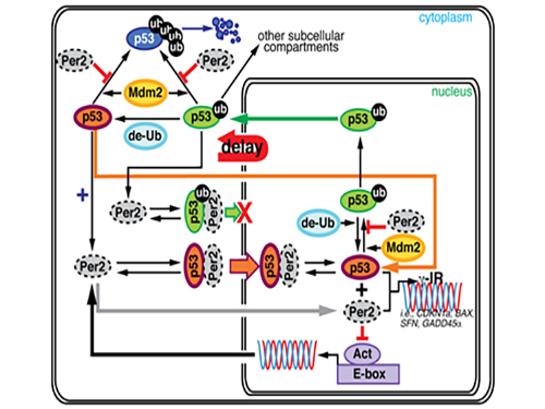
Picture 1. The complex interaction between tumor antigen p53 and Period2 (Per2) which plays a major role in the circadian clock as revealed by mathematical simulations and experiments
Picture 2. A portion of the mathematical model used in the research
Picture 3. Professor Jae Kyoung Kim (third from left) and the Virginia Tech Research Team
2016.11.17 View 8358
Key Interaction between the Circadian Clock and Cancer Identified
Professor Jae Kyoung Kim and his research team from the Department of Mathematical Sciences at KAIST found that the circadian clock drives changes in circadian rhythms of p53 which functions as a tumor suppressor. Using a differential equation, he applied a model-driven mathematical approach to learn the mechanism and role of p53.
Kim’s mathematical modeling has been validated by experimental studies conducted by a research team at Virginia Polytechnic Institute and State University (Virginia Tech) in the United State, which is led by Professor Carla Finkielstein. As a result, the researchers revealed that there is an important link existed between the circadian clock and cancer.
The findings of this research were published online in Proceedings of the National Academy of Sciences of the United States of the America (PNAS) on November 9, 2016.
The circadian clock in our brain controls behavioral and physiological processes within a period of 24 hours, including making us fall asleep at a certain time by triggering the release of the sleep hormone melatonin in our brain, for example, around 9 pm. The clock is also involved in various physiological processes such as cell division, movement, and development.
Disruptions caused by the mismatch of the circadian clock and real time due to chronic late night work, shiftwork, and other similar issues may lead to various diseases such as diabetes, cancer, and heart disease.
In 2014, when Kim met with Finkielstein, her research team succeeded in observing the changes of p53 over a period of 24 hours, but could not understand how the circadian clock controls the 24-hour rhythm of p53. It was difficult to determine p53’s mechanism since its cell regulation system is far more complex than other cells
To solve the problem, Kim set up a computer simulation using mathematical modeling and ran millions of simulations. Instead of the traditional method based on trial and error experiments, mathematical modeling allowed to save a great deal of time, cost, and manpower.
During this process, Kim proved that the biorhythm of p53 and Period2, an important protein in the circadian clock, are closely related. Cells usually consist of a cell nucleus and cytoplasm. While p53 exists in both nucleus and cytoplasm, it becomes more stable and its degradation slows down when it is in the nucleus.
Kim predicted that the Period2 protein, which plays a key role in the functioning of the circadian clock, could influence the nucleus entry of the p53 protein.
Kim’s predictions based on mathematical modeling have been validated by the Virginia team, thereby revealing a strong connection between the circadian clock and cancer.
Researchers said that this research will help explain the cause of different results from numerous anticancer drugs, which are used to normalize the level of p53, when they are administrated at different times and find the most effective dosing times for the drugs.
They also believe that this study will play an important role in identifying the cause of increasing cancer rates in shift-workers whose circadian clocks are unstable and will contribute to the development of more effective treatments for cancer.
Professor Kim said, “This is an exciting thing that my research can contribute to improving the healthy lives of nurses, police officers, firefighters, and the like, who work in shifts against their circadian rhythms. Taking these findings as an opportunity, I hope to see more active interchanges of ideas between biological sciences and mathematical science in Korea.”
This research has been jointly conducted between KAIST and Virginia Tech and supported by the T. J. Park Science Fellowship of POSCO, the National Science Foundation of the United States, and the Young Researcher Program of the National Research Foundation of Korea.
Picture 1. The complex interaction between tumor antigen p53 and Period2 (Per2) which plays a major role in the circadian clock as revealed by mathematical simulations and experiments
Picture 2. A portion of the mathematical model used in the research
Picture 3. Professor Jae Kyoung Kim (third from left) and the Virginia Tech Research Team
2016.11.17 View 8358 -
 Extremely Thin and Highly Flexible Graphene-Based Thermoacoustic Speakers
A joint research team led by Professors Jung-Woo Choi and Byung Jin Cho of the School of Electrical Engineering and Professor Sang Ouk Kim of the Material Science and Engineering Department, all on the faculty of the Korea Advanced Institute of Science and Technology (KAIST), has developed a simpler way to mass-produce ultra-thin graphene thermosacoustic speakers.
Their research results were published online on August 17, 2016 in a journal called Applied Materials & Interfaces. The IEEE Spectrum, a monthly magazine published by the Institute of Electrical and Electronics Engineers, reported on the research on September 9, 2016, in an article titled, “Graphene Enables Flat Speakers for Mobile Audio Systems.” The American Chemical Society also drew attention to the team’s work in its article dated September 7, 2016, “Bringing Graphene Speakers to the Mobile Market.”
Thermoacoustic speakers generate sound waves from temperature fluctuations by rapidly heating and cooling conducting materials. Unlike conventional voice-coil speakers, thermoacoustic speakers do not rely on vibrations to produce sound, and thus do not need bulky acoustic boxes to keep complicated mechanical parts for sound production. They also generate good quality sound in all directions, enabling them to be placed on any surface including curved ones without canceling out sounds generated from opposite sides.
Based on a two-step, template-free fabrication method that involved freeze-drying a solution of graphene oxide flakes and the reduction/doping of oxidized graphene to improve electrical properties, the research team produced a N-doped, three-dimensional (3D), reduced graphene oxide aerogel (N-rGOA) with a porous macroscopic structure that permitted easy modulation for many potential applications.
Using 3D graphene aerogels, the team succeeded in fabricating an array of loudspeakers that were able to withstand over 40 W input power and that showed excellent sound pressure level (SPL), comparable to those of previously reported 2D and 3D graphene loudspeakers.
Choong Sun Kim, the lead author of the research paper and a doctoral student in the School of Electrical Engineering at KAIST, said:
“Thermoacoustic speakers have a higher efficiency when conducting materials have a smaller heat capacity. Nanomaterials such as graphene are an ideal candidate for conductors, but they require a substrate to support their extremely thinness. The substrate’s tendency to lose heat lowers the speakers’ efficiency. Here, we developed 3D graphene aerogels without a substrate by using a simple two-step process. With graphene aerogels, we have fabricated an array of loudspeakers that demonstrated stable performance. This is a practical technology that will enable mass-production of thermosacoustic speakers including on mobile platforms.”
The research paper is entitled “Application of N-Doped Three-Dimensional Reduced Graphene Oxide Aerogel to Thin Film Loudspeaker.” (DOI: 10.1021/acsami.6b03618)
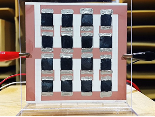
Figure 1: A Thermoacoustic Loudspeaker Consisted of an Array of 16 3D Graphene Aerogels
Figure 2: Two-step Fabrication Process of 3D Reduced Graphene Oxide Aerogel Using Freeze-Drying and Reduction/Doping
Figure 3: X-ray Photoelectron Spectroscopy Graph of the 3D Reduced Graphene Oxide Aerogel and Its Scanning Electron Microscope Image
2016.10.05 View 15283
Extremely Thin and Highly Flexible Graphene-Based Thermoacoustic Speakers
A joint research team led by Professors Jung-Woo Choi and Byung Jin Cho of the School of Electrical Engineering and Professor Sang Ouk Kim of the Material Science and Engineering Department, all on the faculty of the Korea Advanced Institute of Science and Technology (KAIST), has developed a simpler way to mass-produce ultra-thin graphene thermosacoustic speakers.
Their research results were published online on August 17, 2016 in a journal called Applied Materials & Interfaces. The IEEE Spectrum, a monthly magazine published by the Institute of Electrical and Electronics Engineers, reported on the research on September 9, 2016, in an article titled, “Graphene Enables Flat Speakers for Mobile Audio Systems.” The American Chemical Society also drew attention to the team’s work in its article dated September 7, 2016, “Bringing Graphene Speakers to the Mobile Market.”
Thermoacoustic speakers generate sound waves from temperature fluctuations by rapidly heating and cooling conducting materials. Unlike conventional voice-coil speakers, thermoacoustic speakers do not rely on vibrations to produce sound, and thus do not need bulky acoustic boxes to keep complicated mechanical parts for sound production. They also generate good quality sound in all directions, enabling them to be placed on any surface including curved ones without canceling out sounds generated from opposite sides.
Based on a two-step, template-free fabrication method that involved freeze-drying a solution of graphene oxide flakes and the reduction/doping of oxidized graphene to improve electrical properties, the research team produced a N-doped, three-dimensional (3D), reduced graphene oxide aerogel (N-rGOA) with a porous macroscopic structure that permitted easy modulation for many potential applications.
Using 3D graphene aerogels, the team succeeded in fabricating an array of loudspeakers that were able to withstand over 40 W input power and that showed excellent sound pressure level (SPL), comparable to those of previously reported 2D and 3D graphene loudspeakers.
Choong Sun Kim, the lead author of the research paper and a doctoral student in the School of Electrical Engineering at KAIST, said:
“Thermoacoustic speakers have a higher efficiency when conducting materials have a smaller heat capacity. Nanomaterials such as graphene are an ideal candidate for conductors, but they require a substrate to support their extremely thinness. The substrate’s tendency to lose heat lowers the speakers’ efficiency. Here, we developed 3D graphene aerogels without a substrate by using a simple two-step process. With graphene aerogels, we have fabricated an array of loudspeakers that demonstrated stable performance. This is a practical technology that will enable mass-production of thermosacoustic speakers including on mobile platforms.”
The research paper is entitled “Application of N-Doped Three-Dimensional Reduced Graphene Oxide Aerogel to Thin Film Loudspeaker.” (DOI: 10.1021/acsami.6b03618)
Figure 1: A Thermoacoustic Loudspeaker Consisted of an Array of 16 3D Graphene Aerogels
Figure 2: Two-step Fabrication Process of 3D Reduced Graphene Oxide Aerogel Using Freeze-Drying and Reduction/Doping
Figure 3: X-ray Photoelectron Spectroscopy Graph of the 3D Reduced Graphene Oxide Aerogel and Its Scanning Electron Microscope Image
2016.10.05 View 15283 -
 Professor Seyun Kim Identifies a Neuron Signal Controlling Molecule
A research team led by Professor Seyun Kim of the Department of Biological Sciences at KAIST has identified inositol pyrophosphates as the molecule that strongly controls neuron signaling via synaptotagmin.
Professors Tae-Young Yoon of Yonsei University’s Y-IBS and Sung-Hyun Kim of Kyung Hee University’s Department of Biomedical Science also joined the team.
The results were published in the Proceedings of the National Academy of Sciences of the United States of America (PNAS) on June 30, 2016.
This interdisciplinary research project was conducted by six research teams from four different countries and covered a wide scope of academic fields, from neurobiology to super resolution optic imaging.
Inositol pyrophosphates such as 5-diphosphoinositol pentakisphos-phate (5-IP7), which naturally occur in corns and beans, are essential metabolites in the body. In particular, inositol hexakisphosphate (IP6) has anti-cancer properties and is thought to have an important role in cell signaling.
Inositol pentakisphosphate (IP7) differs from IP6 by having an additional phosphate group, which was first discovered 20 years ago. IP7 has recently been identified as playing a key role in diabetes and obesity.
Psychopathy and neurodegenerative diseases are known to result from the disrupted balance of inositol pyrophosphates. However, the role and the mechanism of action of IP7 in brain neurons and nerve transmission remained unknown.
Professor Kim’s team has worked on inositol pyrophosphates for several years and discovered that very small quantities of IP7 control cell-signaling transduction. Professor Yoon of Yonsei University identified IP7 as a much stronger inhibitor of neuron signaling compared to IP6. In particular, IP7 directly suppresses synaptotagmin, one of the key proteins in neuron signaling. Moreover, Professor Kim of Kyung Hee University observed IP7 inhibition in sea horse neurons.
Together, the joint research team identified inositol pyrophosphates as the key switch metabolite of brain-signaling transduction.
The researchers hope that future research on synaptotagmin and IP7 will reveal the mechanism of neuron-signal transduction and thus enable the treatment of neurological disorders.
These research findings were the result of cooperation of various science and technology institutes: KAIST, Yonsei-IBS (Institute for Basic Science), Kyung Hee University, Sungkyunkwan University, KIST, University of Zurich in Switzerland, and Albert-Ludwigs-University Freiburg in Germany.
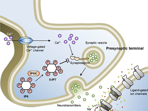
Schematic Image of Controlling the Synaptic Exocytotic Pathway by 5-IP7 , Helping the Understanding of the Signaling Mechanisms of Inositol Pyrophosphates
2016.07.21 View 12857
Professor Seyun Kim Identifies a Neuron Signal Controlling Molecule
A research team led by Professor Seyun Kim of the Department of Biological Sciences at KAIST has identified inositol pyrophosphates as the molecule that strongly controls neuron signaling via synaptotagmin.
Professors Tae-Young Yoon of Yonsei University’s Y-IBS and Sung-Hyun Kim of Kyung Hee University’s Department of Biomedical Science also joined the team.
The results were published in the Proceedings of the National Academy of Sciences of the United States of America (PNAS) on June 30, 2016.
This interdisciplinary research project was conducted by six research teams from four different countries and covered a wide scope of academic fields, from neurobiology to super resolution optic imaging.
Inositol pyrophosphates such as 5-diphosphoinositol pentakisphos-phate (5-IP7), which naturally occur in corns and beans, are essential metabolites in the body. In particular, inositol hexakisphosphate (IP6) has anti-cancer properties and is thought to have an important role in cell signaling.
Inositol pentakisphosphate (IP7) differs from IP6 by having an additional phosphate group, which was first discovered 20 years ago. IP7 has recently been identified as playing a key role in diabetes and obesity.
Psychopathy and neurodegenerative diseases are known to result from the disrupted balance of inositol pyrophosphates. However, the role and the mechanism of action of IP7 in brain neurons and nerve transmission remained unknown.
Professor Kim’s team has worked on inositol pyrophosphates for several years and discovered that very small quantities of IP7 control cell-signaling transduction. Professor Yoon of Yonsei University identified IP7 as a much stronger inhibitor of neuron signaling compared to IP6. In particular, IP7 directly suppresses synaptotagmin, one of the key proteins in neuron signaling. Moreover, Professor Kim of Kyung Hee University observed IP7 inhibition in sea horse neurons.
Together, the joint research team identified inositol pyrophosphates as the key switch metabolite of brain-signaling transduction.
The researchers hope that future research on synaptotagmin and IP7 will reveal the mechanism of neuron-signal transduction and thus enable the treatment of neurological disorders.
These research findings were the result of cooperation of various science and technology institutes: KAIST, Yonsei-IBS (Institute for Basic Science), Kyung Hee University, Sungkyunkwan University, KIST, University of Zurich in Switzerland, and Albert-Ludwigs-University Freiburg in Germany.
Schematic Image of Controlling the Synaptic Exocytotic Pathway by 5-IP7 , Helping the Understanding of the Signaling Mechanisms of Inositol Pyrophosphates
2016.07.21 View 12857 -
 Efficient Methane C-H Bond Activated by KAIST and UPenn Teams
Professor Mu-Hyun Baik of the Chemistry Department at KAIST and his team collaborated with an international team to discover a novel chemical reaction, carbon-hydrogen borylation using methane, and their research results were published in the March 25th issue of Science.
For details, please refer to the following press release from the Institute for Basic Sciences (IBS) in Korea and the University of Pennsylvania in the United States.
Efficient Methane C-H Bond Activation Achieved for the First Time
The Institute for Basic Science, March 24, 2016
Penn Chemists Lay Groundwork for Countless New, Cleaner Uses of Methane
University of Pennsylvania, March 24, 2016
2016.03.25 View 10539
Efficient Methane C-H Bond Activated by KAIST and UPenn Teams
Professor Mu-Hyun Baik of the Chemistry Department at KAIST and his team collaborated with an international team to discover a novel chemical reaction, carbon-hydrogen borylation using methane, and their research results were published in the March 25th issue of Science.
For details, please refer to the following press release from the Institute for Basic Sciences (IBS) in Korea and the University of Pennsylvania in the United States.
Efficient Methane C-H Bond Activation Achieved for the First Time
The Institute for Basic Science, March 24, 2016
Penn Chemists Lay Groundwork for Countless New, Cleaner Uses of Methane
University of Pennsylvania, March 24, 2016
2016.03.25 View 10539 -
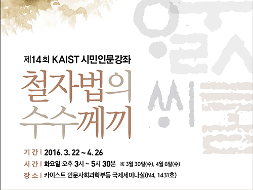 Public Lectures on the Korean Language and Alphabet
The School of Humanities and Social Sciences at KAIST will offer public lectures on the Korean language and alphabet, Hangul, from March 22, 2016 to April 26, 2016.
The lectures, which are entitled “The Riddle of Hangul,” will take place on campus in Daejeon.
A total of six lectures will be held on such topics as the origin of Korean, the grammar of ancient Korean in the Chosun Dynasty (1392-1897), and subsequent developments in contemporary Korean.
Professor Jung-Hoon Kim, who is responsible for organizing the public lecture program, said, “The audience will have an interesting opportunity to understand the history of Korean and its mechanism, while reviewing the unique spelling system of Hangul. I hope many people will show up for these wonderful classes.”
For further information and registration, please visit: http://hss.kaist.ac.kr. All lectures, available only in Korean, are free and open to the public.
2016.03.15 View 9996
Public Lectures on the Korean Language and Alphabet
The School of Humanities and Social Sciences at KAIST will offer public lectures on the Korean language and alphabet, Hangul, from March 22, 2016 to April 26, 2016.
The lectures, which are entitled “The Riddle of Hangul,” will take place on campus in Daejeon.
A total of six lectures will be held on such topics as the origin of Korean, the grammar of ancient Korean in the Chosun Dynasty (1392-1897), and subsequent developments in contemporary Korean.
Professor Jung-Hoon Kim, who is responsible for organizing the public lecture program, said, “The audience will have an interesting opportunity to understand the history of Korean and its mechanism, while reviewing the unique spelling system of Hangul. I hope many people will show up for these wonderful classes.”
For further information and registration, please visit: http://hss.kaist.ac.kr. All lectures, available only in Korean, are free and open to the public.
2016.03.15 View 9996 -
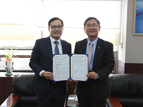 Meditox Donates 600 Million KRW Scholarship
On February 17, a Korean biopharmaceutical company Meditox, headed by Chief Executive Officer (CEO) Hyun-Ho Jeong, signed a memorandum of understanding (MOU) with KAIST to establish the “Meditox Fellowship” and donated a total of 600 million Korean won (KRW) to the university to assist in promoting more scientists in the field of biology.
Meditox CEO Hyun-Ho Jeong, KAIST President Steve Kang, Dean of Life Science and Bioengineering College Jung-Hoe Kim, and Dean of the Department of Biological Sciences Byung-Ha Oh participated in the agreement ceremony.
According to the MOU, Meditox will donate 60,000,000 KRW over a ten year period, from which KAIST can draw on to grant scholarships for master’s and doctoral students.
The “Meditox Fellowship” will support promising and enthusiastic students whose finances limit their studies. The first scholarship students for 2016 were: Kwang-Uk Min, In-suk Yeo, Sung-ryung- Lee, Si-on Lee, and Jung-hyun Kim.
Meditox CEO Jeong, who graduated from KAIST’s Department of Biological Sciences, said, "I felt it was important to start the Meditox Fellowship at my alma mater to contribute to the cultivation of outstanding scientists in the field of biological sciences."
He also said that he would plan to launch projects that aim to support not only those who receive the scholarship but also the development of Korea’s biological sciences in general.
President Steve Kang (right) and Chief Executive Officer Hyun-Ho Jeong (left) of Meditox hold the signed memorandum of understanding together.
2016.02.18 View 11624
Meditox Donates 600 Million KRW Scholarship
On February 17, a Korean biopharmaceutical company Meditox, headed by Chief Executive Officer (CEO) Hyun-Ho Jeong, signed a memorandum of understanding (MOU) with KAIST to establish the “Meditox Fellowship” and donated a total of 600 million Korean won (KRW) to the university to assist in promoting more scientists in the field of biology.
Meditox CEO Hyun-Ho Jeong, KAIST President Steve Kang, Dean of Life Science and Bioengineering College Jung-Hoe Kim, and Dean of the Department of Biological Sciences Byung-Ha Oh participated in the agreement ceremony.
According to the MOU, Meditox will donate 60,000,000 KRW over a ten year period, from which KAIST can draw on to grant scholarships for master’s and doctoral students.
The “Meditox Fellowship” will support promising and enthusiastic students whose finances limit their studies. The first scholarship students for 2016 were: Kwang-Uk Min, In-suk Yeo, Sung-ryung- Lee, Si-on Lee, and Jung-hyun Kim.
Meditox CEO Jeong, who graduated from KAIST’s Department of Biological Sciences, said, "I felt it was important to start the Meditox Fellowship at my alma mater to contribute to the cultivation of outstanding scientists in the field of biological sciences."
He also said that he would plan to launch projects that aim to support not only those who receive the scholarship but also the development of Korea’s biological sciences in general.
President Steve Kang (right) and Chief Executive Officer Hyun-Ho Jeong (left) of Meditox hold the signed memorandum of understanding together.
2016.02.18 View 11624 -
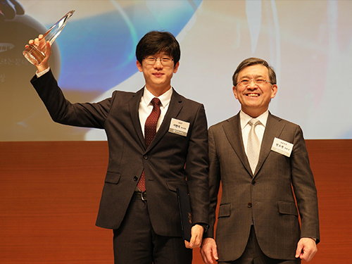 Ph.D. Candidate Seo Wins the Human Tech Paper Award
Hyun-Suk Seo, a doctoral student of KAIST’s Department of Electrical Engineering, received the grand prize of the “22nd Human Tech Paper Award” on February 3, 2016 from Samsung Electronics Co., Ltd.
Seo was the first to receive this prize ever since the Human Tech Paper Award was established 22 years ago. Until last year, the highest prize awarded for KAIST was a gold one.
The “Human Tech Paper Award” was established in 1994 by Samsung Electronics to discover and support outstanding scientists in the field of electrical engineering.
Entitled “Self-Gated Cardiac Cine MRI Using Phase Information,” Seo’s paper presented a technology that would reduce discomforts and inconveniences experienced by patients who take a magnetic resonance imaging (MRI).
This technology uses the speed changes of aorta and the abdominal movements of body to obtain the phase changes of magnetic resonance signals so that MRIs may be taken despite the organs’ movements.
Seo commented on his research, “I wanted to develop a technique that can make MRI a more comfortable experience. I will continue my research on this subject and hope to serve the needs of the society.”
In addition, the “Special Award,” which is given to schools, was awarded to KAIST. KAIST’s Department of Electrical Engineering has also been named the department that has received the second most awards (15 awards) this year.
Oh-Hyun Kwon, Vice President of Samsung Electronics, Steve Kang, President of KAIST, and Nak-In Seo, President of Seoul National University, participated in the event.
Picture: Hyun-Suk Seo (left), the recipient of the grand prize of the 2016 Human Tech Paper Award, and Oh-Hyun Kwon (right), Vice President of Samsung Electronics
2016.02.06 View 10710
Ph.D. Candidate Seo Wins the Human Tech Paper Award
Hyun-Suk Seo, a doctoral student of KAIST’s Department of Electrical Engineering, received the grand prize of the “22nd Human Tech Paper Award” on February 3, 2016 from Samsung Electronics Co., Ltd.
Seo was the first to receive this prize ever since the Human Tech Paper Award was established 22 years ago. Until last year, the highest prize awarded for KAIST was a gold one.
The “Human Tech Paper Award” was established in 1994 by Samsung Electronics to discover and support outstanding scientists in the field of electrical engineering.
Entitled “Self-Gated Cardiac Cine MRI Using Phase Information,” Seo’s paper presented a technology that would reduce discomforts and inconveniences experienced by patients who take a magnetic resonance imaging (MRI).
This technology uses the speed changes of aorta and the abdominal movements of body to obtain the phase changes of magnetic resonance signals so that MRIs may be taken despite the organs’ movements.
Seo commented on his research, “I wanted to develop a technique that can make MRI a more comfortable experience. I will continue my research on this subject and hope to serve the needs of the society.”
In addition, the “Special Award,” which is given to schools, was awarded to KAIST. KAIST’s Department of Electrical Engineering has also been named the department that has received the second most awards (15 awards) this year.
Oh-Hyun Kwon, Vice President of Samsung Electronics, Steve Kang, President of KAIST, and Nak-In Seo, President of Seoul National University, participated in the event.
Picture: Hyun-Suk Seo (left), the recipient of the grand prize of the 2016 Human Tech Paper Award, and Oh-Hyun Kwon (right), Vice President of Samsung Electronics
2016.02.06 View 10710 -
 ISCN and GULF Share Best Practices Report
The International Sustainable Campus Network (ISCN) and the Global University Leaders Forum (GULF) co-hosted a conference at the 2016 World Economic Forum held on January 20-23, 2016 in Davos, Switzerland, to present exemplary campus sustainability case studies provided by the world’s leading universities.
A total of 20 universities, including KAIST, Harvard University, University of Oxford, Yale University, the National University of Singapore, the Hong Kong University of Science and Technology, and the Swiss Federal Institute of Technology (Zurich), reported on their endeavors to demonstrate sustainable development in higher education in three different panels at the conference: Developing Skills and Building Capacities, Collaborating to Catalyze Change, and Innovating for Efficient Built Environments.
President Sung-Mo Kang of KAIST gave a presentation on the Saudi Aramco-KAIST CO2 Management Center as a sustainable development model for KAIST.
KAIST and Saudi Aramco, the world’s leading fossil-fuel provider, joined forces in 2013 to establish a joint research center on the reduction and management of carbon dioxide (CO2) emissions, a major driver of climate change.
The research center, located at the KAIST campus in Daejeon, South Korea, is currently sponsoring ten research projects involving more than 20 doctoral-level researchers and over 100 students.
The goal of the center is to develop materials for more energy-efficient CO2 capture, catalysts and processes for converting CO2 into valuable products, novel storage methods, and system-level analyses of major CO2 emitting industries to suggest industry-specific CO2 reduction strategies including energy efficiency improvement.
The center’s work also includes analyzing the impact of potential government or industry-wide policies in the face of uncertainties, some of which are technological and economic as well as political. Besides its research activities, the center has also sponsored seminars and workshops throughout the year to raise awareness of the importance of CO2 management in building a sustainable future.
President Kang said that, from the beginning, the center has prompted researchers and students with different academic backgrounds and skill sets to work together to find integrative and systematic solutions to address real problems of critical importance to the world’s sustainability.
ISCN is a global non-profit association of leading colleges and universities representing over 20 countries, working together to holistically integrate sustainability into campus operations, research, and teaching. As of now, more 75 universities worldwide are the members of ISCN.
The GULF is composed of the presidents of the top 25 universities in the world. The World Economic Forum created it in 2006 to offer a non-competitive platform for high-level dialogue in academia. KAIST is the only Korean GULF member.
For the full report of the 2016 ISCN and GULF conference, go to http://www.international-sustainable-campus-network.org/downloads/general/441-2016-iscn-gulf-best-practice-report/file.
2016.01.25 View 11070
ISCN and GULF Share Best Practices Report
The International Sustainable Campus Network (ISCN) and the Global University Leaders Forum (GULF) co-hosted a conference at the 2016 World Economic Forum held on January 20-23, 2016 in Davos, Switzerland, to present exemplary campus sustainability case studies provided by the world’s leading universities.
A total of 20 universities, including KAIST, Harvard University, University of Oxford, Yale University, the National University of Singapore, the Hong Kong University of Science and Technology, and the Swiss Federal Institute of Technology (Zurich), reported on their endeavors to demonstrate sustainable development in higher education in three different panels at the conference: Developing Skills and Building Capacities, Collaborating to Catalyze Change, and Innovating for Efficient Built Environments.
President Sung-Mo Kang of KAIST gave a presentation on the Saudi Aramco-KAIST CO2 Management Center as a sustainable development model for KAIST.
KAIST and Saudi Aramco, the world’s leading fossil-fuel provider, joined forces in 2013 to establish a joint research center on the reduction and management of carbon dioxide (CO2) emissions, a major driver of climate change.
The research center, located at the KAIST campus in Daejeon, South Korea, is currently sponsoring ten research projects involving more than 20 doctoral-level researchers and over 100 students.
The goal of the center is to develop materials for more energy-efficient CO2 capture, catalysts and processes for converting CO2 into valuable products, novel storage methods, and system-level analyses of major CO2 emitting industries to suggest industry-specific CO2 reduction strategies including energy efficiency improvement.
The center’s work also includes analyzing the impact of potential government or industry-wide policies in the face of uncertainties, some of which are technological and economic as well as political. Besides its research activities, the center has also sponsored seminars and workshops throughout the year to raise awareness of the importance of CO2 management in building a sustainable future.
President Kang said that, from the beginning, the center has prompted researchers and students with different academic backgrounds and skill sets to work together to find integrative and systematic solutions to address real problems of critical importance to the world’s sustainability.
ISCN is a global non-profit association of leading colleges and universities representing over 20 countries, working together to holistically integrate sustainability into campus operations, research, and teaching. As of now, more 75 universities worldwide are the members of ISCN.
The GULF is composed of the presidents of the top 25 universities in the world. The World Economic Forum created it in 2006 to offer a non-competitive platform for high-level dialogue in academia. KAIST is the only Korean GULF member.
For the full report of the 2016 ISCN and GULF conference, go to http://www.international-sustainable-campus-network.org/downloads/general/441-2016-iscn-gulf-best-practice-report/file.
2016.01.25 View 11070 -
 IdeasLab Presents Biotechnology Solutions for Aging Populations at 2016 Davos Forum
KAIST researchers will discuss how biological sciences and health technologies can address challenges and opportunities posed by aging populations in an era of increasing longevity.
Many countries around the world today are experiencing the rapid growth of aging populations, with a decline in fertility rate and longer life expectancy.
At this year's Annual Meeting of the World Economic Forum (a.k.a. Davos Forum) on January 20-23, 2016 in Davos-Klosters, Switzerland, four researchers in the field of biological sciences and biotechnology at the Korea Advanced Institute of Science and Technology (KAIST) will discuss the implications of an aging population and explore possible solutions to provide better health care services to the elderly.
KAIST will host an IdeasLab twice on the theme "Biotechnology Solutions for Ageing Populations" on January 21st and 23rd, respectively.
Professor Byung-Kwan Cho of the Biological Sciences Department will give a presentation on "Rejuvenation via the Microbiome," explaining how microorganisms in the human gut play an important role in preventing aging, or even rejuvenating it.
Distinguished Professor Sang Yup Lee of the Chemical and Biomolecular Engineering Department will talk about "Traditional Medicine Reimagined through Modern Systems Biology." Professor Lee will introduce his research results published in Nature Biotechnology (March 6, 2015) and some more new results. He discovered the mechanisms of traditional oriental medicine's (TOM) efficacy by applying systems biology to study structural similarities between natural and nontoxic multi-compounds in the medicine and human metabolites. He will discuss TOM's multi-target approach, which is based on the synergistic combinations of multi-compounds to treat symptoms of a disease, can contribute to the development of new drugs, cosmetics, and nutrients.
Professor Youn-Kyung Lim of the Industrial Design Department will speak about a mobile and the Internet of Things-based health care service called "Dr. M" in her presentation on "Advanced Mobile Healthcare Systems."
Professor Daesoo Kim of the Biological Sciences Department will share his research on human's happiness and greed in the context of nueroscience and behavioral and biological sciences in a talk entitled "A Neural Switch for Being Happy with Less on a Crowded Planet."
KAIST has hosted IdeasLabs several times at the Summer Davos Forum in China, but this is the first time it will participate in the Davos Forum in January.
Professor Lee said, "Just like climate change, the issue of how to address aging populations has become a major global issue. We will share some exciting research results and hope to have in depth discussion on this issue with the leaders attending the Davos Forum. KAIST will engage actively in finding solutions that benefit not only Korea but also the international community."
2016.01.19 View 12431
IdeasLab Presents Biotechnology Solutions for Aging Populations at 2016 Davos Forum
KAIST researchers will discuss how biological sciences and health technologies can address challenges and opportunities posed by aging populations in an era of increasing longevity.
Many countries around the world today are experiencing the rapid growth of aging populations, with a decline in fertility rate and longer life expectancy.
At this year's Annual Meeting of the World Economic Forum (a.k.a. Davos Forum) on January 20-23, 2016 in Davos-Klosters, Switzerland, four researchers in the field of biological sciences and biotechnology at the Korea Advanced Institute of Science and Technology (KAIST) will discuss the implications of an aging population and explore possible solutions to provide better health care services to the elderly.
KAIST will host an IdeasLab twice on the theme "Biotechnology Solutions for Ageing Populations" on January 21st and 23rd, respectively.
Professor Byung-Kwan Cho of the Biological Sciences Department will give a presentation on "Rejuvenation via the Microbiome," explaining how microorganisms in the human gut play an important role in preventing aging, or even rejuvenating it.
Distinguished Professor Sang Yup Lee of the Chemical and Biomolecular Engineering Department will talk about "Traditional Medicine Reimagined through Modern Systems Biology." Professor Lee will introduce his research results published in Nature Biotechnology (March 6, 2015) and some more new results. He discovered the mechanisms of traditional oriental medicine's (TOM) efficacy by applying systems biology to study structural similarities between natural and nontoxic multi-compounds in the medicine and human metabolites. He will discuss TOM's multi-target approach, which is based on the synergistic combinations of multi-compounds to treat symptoms of a disease, can contribute to the development of new drugs, cosmetics, and nutrients.
Professor Youn-Kyung Lim of the Industrial Design Department will speak about a mobile and the Internet of Things-based health care service called "Dr. M" in her presentation on "Advanced Mobile Healthcare Systems."
Professor Daesoo Kim of the Biological Sciences Department will share his research on human's happiness and greed in the context of nueroscience and behavioral and biological sciences in a talk entitled "A Neural Switch for Being Happy with Less on a Crowded Planet."
KAIST has hosted IdeasLabs several times at the Summer Davos Forum in China, but this is the first time it will participate in the Davos Forum in January.
Professor Lee said, "Just like climate change, the issue of how to address aging populations has become a major global issue. We will share some exciting research results and hope to have in depth discussion on this issue with the leaders attending the Davos Forum. KAIST will engage actively in finding solutions that benefit not only Korea but also the international community."
2016.01.19 View 12431 -
 Professor Joonho Choe Appointed as the President of the KSMCB
Professor Joonho Choe of the Biological Sciences Department at KAIST has been elected the 25th president of Korean Society for Molecular and Cellular Biology (KSMCB).
His presidency will last one year, beginning on January 1, 2016.
Established in 1989, the Society has served as the largest academic gathering in the field of life sciences, holding an international conference every fall. It has more than 12,400 fellows.
Professor Choe served as the vice president of KSMC as well as the editor of its journal, Molecules and Cells.
He said, “The 2016 International Conference of the KSMCB will take place on October 12-14, 2016 at the COEX Convention and Exhibition Hall in Seoul. This year, we are preparing 20 symposiums and will invite four international renowned keynote speakers in the field including a Nobel Laureate. We hope many people, students and young researchers in particular, from academia and industry will join the conference.”
Professor Choe received his doctoral degree from the University of California, Los Angeles (UCLA) after graduating from Seoul National University with his bachelor and master’s degrees.
2016.01.05 View 9819
Professor Joonho Choe Appointed as the President of the KSMCB
Professor Joonho Choe of the Biological Sciences Department at KAIST has been elected the 25th president of Korean Society for Molecular and Cellular Biology (KSMCB).
His presidency will last one year, beginning on January 1, 2016.
Established in 1989, the Society has served as the largest academic gathering in the field of life sciences, holding an international conference every fall. It has more than 12,400 fellows.
Professor Choe served as the vice president of KSMC as well as the editor of its journal, Molecules and Cells.
He said, “The 2016 International Conference of the KSMCB will take place on October 12-14, 2016 at the COEX Convention and Exhibition Hall in Seoul. This year, we are preparing 20 symposiums and will invite four international renowned keynote speakers in the field including a Nobel Laureate. We hope many people, students and young researchers in particular, from academia and industry will join the conference.”
Professor Choe received his doctoral degree from the University of California, Los Angeles (UCLA) after graduating from Seoul National University with his bachelor and master’s degrees.
2016.01.05 View 9819 -
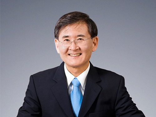
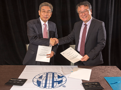 Prof. Jae-Kyu Lee Campaigns on "Bright Internet" Worldwide
Professor Jae-Kyu Lee (pictured on the right) from the College of Business at KAIST is one step closer to fulfilling his dream of achieving the “Bright Internet,” a campaign that he first proposed as he became the president of the Association for Information Systems (AIS) in June 2015.
On December 12, 2015, Professor Lee signed a memorandum of understanding (MOU) at a convention center in Fort Worth, Texas, between the AIS and the International Telecommunication Union (ITU)—a specialized agency of the United Nations that is responsible for issues related to information and communication technologies—on a collaborative research and development program to make the Internet safer for everyone.
The MOU pursues building a trusted international information and communication technology (ICT) infrastructure by proposing telecommunication policies, developing international standards, and organizing interdisciplinary conferences.
The Bright Internet is an initiative to protect online users from cyber terrors, privacy breaches, and cyber-crimes. Further, it involves putting accountability to those who initiate or deliver cyber threats, thereby eliminating the possible source of Internet related crimes.
Following the MOU agreement, Prof. Lee delivered a speech on his campaign at the 2015 International Conference on Information Systems and received positive responses from the audience.
The Bright Internet campaign has been selected as visions of various ICT organizations worldwide including the Korea Society of Management Information System and the International Federation of Information Processing. KAIST and Tsinghua University in China adopted it as an academic topic for research and teaching.
Prof. Lee claimed that the Internet should be used in a manner based on the values of trust, ethics, and decorum. He further noted that it is important to build Internet environments that not only protect individuals from cyber threats or attacks, but also hold those who commit online crimes accountable for their actions.
2015.12.28 View 10884
Prof. Jae-Kyu Lee Campaigns on "Bright Internet" Worldwide
Professor Jae-Kyu Lee (pictured on the right) from the College of Business at KAIST is one step closer to fulfilling his dream of achieving the “Bright Internet,” a campaign that he first proposed as he became the president of the Association for Information Systems (AIS) in June 2015.
On December 12, 2015, Professor Lee signed a memorandum of understanding (MOU) at a convention center in Fort Worth, Texas, between the AIS and the International Telecommunication Union (ITU)—a specialized agency of the United Nations that is responsible for issues related to information and communication technologies—on a collaborative research and development program to make the Internet safer for everyone.
The MOU pursues building a trusted international information and communication technology (ICT) infrastructure by proposing telecommunication policies, developing international standards, and organizing interdisciplinary conferences.
The Bright Internet is an initiative to protect online users from cyber terrors, privacy breaches, and cyber-crimes. Further, it involves putting accountability to those who initiate or deliver cyber threats, thereby eliminating the possible source of Internet related crimes.
Following the MOU agreement, Prof. Lee delivered a speech on his campaign at the 2015 International Conference on Information Systems and received positive responses from the audience.
The Bright Internet campaign has been selected as visions of various ICT organizations worldwide including the Korea Society of Management Information System and the International Federation of Information Processing. KAIST and Tsinghua University in China adopted it as an academic topic for research and teaching.
Prof. Lee claimed that the Internet should be used in a manner based on the values of trust, ethics, and decorum. He further noted that it is important to build Internet environments that not only protect individuals from cyber threats or attacks, but also hold those who commit online crimes accountable for their actions.
2015.12.28 View 10884